EP0428601B1 - System for measuring partial discharges - Google Patents
System for measuring partial discharges Download PDFInfo
- Publication number
- EP0428601B1 EP0428601B1 EP89909403A EP89909403A EP0428601B1 EP 0428601 B1 EP0428601 B1 EP 0428601B1 EP 89909403 A EP89909403 A EP 89909403A EP 89909403 A EP89909403 A EP 89909403A EP 0428601 B1 EP0428601 B1 EP 0428601B1
- Authority
- EP
- European Patent Office
- Prior art keywords
- signal
- acquisition
- voltage
- mat
- partial discharges
- Prior art date
- Legal status (The legal status is an assumption and is not a legal conclusion. Google has not performed a legal analysis and makes no representation as to the accuracy of the status listed.)
- Expired - Lifetime
Links
Images


Classifications
-
- G—PHYSICS
- G01—MEASURING; TESTING
- G01R—MEASURING ELECTRIC VARIABLES; MEASURING MAGNETIC VARIABLES
- G01R31/00—Arrangements for testing electric properties; Arrangements for locating electric faults; Arrangements for electrical testing characterised by what is being tested not provided for elsewhere
- G01R31/12—Testing dielectric strength or breakdown voltage ; Testing or monitoring effectiveness or level of insulation, e.g. of a cable or of an apparatus, for example using partial discharge measurements; Electrostatic testing
Definitions
- the present invention relates to a partial discharge measurement system.
- Partial discharges occur in equipment used in high voltage installations of the transport and distribution of electrical energy, for example.
- an element In a dielectric chain subjected to high voltage, an element is the site of a breakdown and the energy corresponding to the capacitive load of this element is dissipated in the form of an oscillation at high frequency.
- the other elements of the chain retain their integrity, so that the partial discharge does not cause breakdown of the assembly.
- Patent document DE-A-36 12 234 describes a system of the same type.
- US-A-4,757,263 describes an apparatus for monitoring different electrical quantities in the same installation, but these quantities are rather continuous, unlike the signals generated by partial discharges which are impulsive and unpredictable.
- the present invention specifically relates to a partial discharge measurement system meeting this need.
- the partial discharge measurement system of the present invention comprises first and second acquisition devices each comprising a signal input, a signal shaping device supplying a signal value, a multiplexer making it possible to supply successively on a common channel for a signal storage and processing system, of the signal values supplied by the various acquisition devices. It is characterized in that said first acquisition devices receive different partial discharge signals from different points of an installation and in that there is provided an acquisition triggering device responding to the existence of a partial discharge signal supplied by a comparator when the input level of at least one acquisition device exceeds a defined threshold and providing an acquisition control signal, said signal storage and processing system responding to the signal acquisition control and then performing an acquisition cycle during which it stores the signal values supplied by the various acquisition devices, through the multiplexer.
- Such a system allows asynchronous recording of groups of signal values each corresponding to one of successive partial discharges. However, it is important to locate partial discharges over time.
- one of said second acquisition devices provides instant measurement of the AC voltage of the distribution network.
- said voltage acquisition device comprises means conditioning the supply of the measurement of the alternating voltage of the distribution network by the presence of said acquisition control signal.
- said voltage acquisition triggering device comprises means sensitive to the appearance of a maximum voltage value on the input of said voltage acquisition device and then providing a signal additional acquisition control, said signal storage and processing system responding to the additional acquisition control signal and then performing an acquisition cycle.
- the signal storage and processing system will be a suitably programmed trade computer. Signal values will be converted to digital form, preferably after multiplexing.
- FIG. 1 represents an equipment in Z tests connected between a high voltage HV power supply line and ground, as well as, to obtain voltage measurement signals, a capacitive voltage divider composed capacitors C1 and C2, at the common point of which is available, on the output st, a voltage signal in the form of an alternating voltage whose value is a fraction of the high voltage, and that, to obtain measurement signals of partial discharges, a voltage divider comprising, in a known manner, a capacitor C3 and an impedance zm at the common point of which is available, on the output sd, on the occasion of each partial discharge occurring in the equipment Z, a partial discharge pulse signal having a general form of damped sinusoidal oscillation.
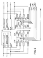
- FIG. 2 represents, as test equipment, a three-phase transformer TR, with its three primary triangular windings ep1, ep2, ep3, connected to the three wires of a low voltage line a, b, c, and its three secondary star windings es1, es2, es3 connected to four wires of a distribution line A , B, C, N.
- TR three-phase transformer TR
- capacitors C3p1, C3p2, C3p3, C3s1, c3s2, c3s3 and c3n playing the role of the capacitor C3 and the impedances zmp1 ..., zms3 and zmn, playing the role of the impedance zm, vis-à-vis partial discharge signal outputs sdp1 to sds3 and sdn.
- the capacitors c1p and c2p play the role of the capacitors C1, C2, vis-à-vis a voltage signal output.
- the partial discharge acquisition device MAD of FIG. 3 processes any of the partial discharge signals and formats it; moreover, it contributes to the development of an acquisition control signal.
- This device from an input EN, to which the output sds1 of FIG. 2 is connected, for example, comprises a first inverting amplifier ai1, operating a level adaptation.
- the resulting signal at the output of the amplifier ai1, is applied to an input of two comparators, ce1 and ce2 also receiving two reference voltages V + and V-. If the output signal of the amplifier ai1 exceeds the voltage V +, the comparator ce1 provides a signal which passes through the gate pt1 and changes position the flip-flop bs1. This then provides a signal vd1 which activates a peak detector DC1.
- a complementary signal vr1 blocks the gate pt2.
- the peak detector DC1 which receives the output signal from the amplifier ai1 through an additional inverting amplifier with unity gain ai2, maintains on its output sd1 a signal level which corresponds to the maximum positive level reached by the signal entry.
- the device provides a DP signal indicating the detection of a partial discharge. The level reached by partial discharge is read by supplying an AC signal. Together with the signal vd1, the signal AC unlocks the door pt3 and causes the operation of a switch cm1 closing a contact ct1, so that the signal level present on the output sd1 of the peak detector DC1 is supplied on the output ST of the device.
- the operation is the same, the peak detector DC2 directly receiving the output signal from the amplifier ai1 and therefore processing a signal of the same polarity as the peak detector DC1, while the auxiliary amplifier ai3 with unity gain inverts the output signal sd2 from the peak detector DC2 to provide a signal sd2 'of the polarity of the input signal on the ST output.
- the DP signal is supplied by the door po as before.
- the device MAD of FIG. 3 on the appearance of a partial discharge signal, selects the polarity of the first half-wave of this signal and, for this polarity, retains the value of peak voltage reached which is prepared as value signal, while a partial discharge presence signal is provided to request an acquisition.
- the acquisition allows the signal value to be read from the ST output.
- a signal RZ puts the flip-flop bs1 or bs2 and the peak detector DC1 or DC2 to rest and the device returns to its initial state.
- the AC supply voltage acquisition device MAT of FIG. 4 formats the voltage signals coming for example from the output st of the assembly of FIG. 2 and triggers the acquisition when the voltage passes through a positive maximum or negative.
- the shaping of the voltage signal is carried out mainly using a sampling circuit ECH which receives the signal supplied to the input ENT of the device through a step-down impedance amplifier with unity gain ae.
- the signal DP supplied by any one of the devices in accordance with FIG. 3 when a partial discharge is signaled changes position a flip-flop which validates the sampling circuit ECH. This stores the value of the voltage supplied to it at this time by the amplifier ae and maintains the value recorded on its output se.
- the output signal from the flip-flop be allows the AC signal to pass through the gate pe and cause the switch to operate, which then closes its contact ce1, providing the sampled voltage value on the STT output.
- this part VT of the device of FIG. 4 works in addition to MAD devices such as that of FIG. 3 and provides, on the occasion of each partial discharge, a value of the alternating voltage recorded on one of the conductors of the high voltage line supplying the equipment under test; this will locate the partial discharge within half a period of this AC voltage.
- the invention also provides for detecting and recording the positive and negative maxima of the alternating voltage, in order to allow localization over time of the partial discharges with respect to the half-periods of the alternating voltage.
- the input voltage is applied, via a step-down amplifier with unit gain impedance at1, to a comparator cmt1 also receiving a voltage Vr +.
- This voltage is relatively low and makes it possible to orient the positive and negative alternations of the alternating voltage towards the circuits intended to process them.
- the comparator cmt1 when this voltage is exceeded, provides a signal ve1 which validates the maximum detection device DM1.
- One such device is sold by "Precision Monolithics, Inc.” under the reference PKD-O1. This device monitors the signal supplied to it by the amplifier at1, with the appropriate time constants, and supplies a signal mx1 when the amplitude of this signal begins to decrease.
- this signal mx1 provides a signal MAX indicating a maximum (positive, in this case) of the alternating voltage evaluated and requesting an acquisition.
- the device DM1 samples the alternating signal and maintains on its output sm1 the sample obtained at the time when it supplies the signal mx1.
- the mx1 signal through the px1 gate, validates the py1 gate.
- a signal CR is supplied to the device of FIG. 4 and, by the gate py1, it actuates the switch cx1 which closes the contact tx1. The maximum positive value of the alternating voltage is thus transferred to the STT output.
- the input voltage reproduced at the output of the amplifier at1 is also applied to a comparator cmt2 detecting the crossing of a threshold Vr- and consequently supplying a signal ve2 validating the device DM2 identical to the device DM1.
- This DM2 device receives the input voltage via an at2 unit gain reversing amplifier. Its operation is thus the same as that of the DM1 device. It thus supplies a signal mx2 when the input voltage passes through a negative maximum and the gate pm then supplies the acquisition request signal MAX.
- the sampled value maintained on the output sm2 of the device DM2 is inverted by the inverting amplifier at3.
- the door px2 being validated by the signals ve2 and max2 itself validates the door py2 which transmits the signal CR to the switch CX2 which closes the contact tx2, and the value maximum negative of the input voltage of the device of FIG. 4 is transmitted on its STT output.
- the device MAT of FIG. 4 thus causes an acquisition of maximum voltage at each half-period of the supply voltage.
- the counting of these half-periods will make it possible to follow the course of time until the appearance of an acquisition of partial discharge, to locate this partial discharge in a defined half-period.
- the location within the half-period will result, it will be recalled, from the voltage value coming from the sampling device ECH, compared with the values of neighboring maximum voltages.
- the logic acquisition control device LA of FIG. 5 serves as an interface between MAD and MAT devices conforming to FIGS. 3 and 4 and a general-purpose computer suitably programmed ORD. If the flip-flop bc2 is at rest, a signal DP coming from a device such as that of FIG. 3, through the door pc1, changes position the flip-flop bc1 which blocks a door pc2. The flip-flop bc1 supplies the signal AC mentioned above by which each MAD device such as that of FIG. 3 provides on its output ST a partial discharge signal corresponding to the peak amplitude of the first alternation of the pulse signal caused by the partial discharge, while the device MAT in FIG. 4 provides the value of the alternating voltage at this instant, maintained by the sampling circuit ECH.
- the AC signal is also transmitted to the computer ORD, to cause the execution of an acquisition cycle by which the values thus presented are recorded. Then, with a sufficient delay, supplied by a delay stage ER, the device LA supplies the signal RZ, which puts the flip-flop bc1 at rest at the same time as the devices MAD and MAT of FIGS. 3 and 4.
- the gate pc2 leads and the flip-flop bc2 changes position, blocking the gate pc1 and supplying the signal CR.
- An acquisition cycle similar to the previous 5 is accomplished. It concludes with the supply of a signal RZ 'by the delay circuit ER' of the module LA itself, which puts the flip-flop bc2 in its initial position, as well as the maximum detector DM1 or DM2 of the device of FIG. 4 .
- FIG. 6, finally, gives a diagram illustrating an ORD computer, provided with an INT interface containing an MTX multiplexer, as well as an analog-digital converter CAN.
- the acquisition devices MAD and MAT of FIGS. 3 and 4 and the acquisition control logic LA of FIG. 5 are connected to the interface INT.
- the INT interface converts the CR and AC signals of the LA logic into interrupt requests in exchange for which the computer ORD addresses the MAD / MAT devices, via the MTX multiplexer and obtains, by means of the interposed CAN converter, digital values corresponding to the analog quantities available on the ST and STT outputs.
- the CR and AC signals can moreover cause identical acquisition cycles in which, using the configuration illustrated in FIG.
Abstract
Description
La présente invention a pour objet un système de mesure de décharges partielles.The present invention relates to a partial discharge measurement system.
Les décharges partielles se produisent dans les équipements utilisés dans les installations à haute tension des réseaux de transport et de distribution d'énergie électrique, par exemple. Dans une chaîne diéletrique soumise à la haute tension, un élément est le siège d'un claquage et l'énergie correspondant à la charge capacitive de cet élément est dissipée sous la forme d'une oscillation à fréquence élevée. Les autres éléments de la chaîne conservent leur intégrité, de sorte que la décharge partielle n'entraîne pas de claquage de l'ensemble.Partial discharges occur in equipment used in high voltage installations of the transport and distribution of electrical energy, for example. In a dielectric chain subjected to high voltage, an element is the site of a breakdown and the energy corresponding to the capacitive load of this element is dissipated in the form of an oscillation at high frequency. The other elements of the chain retain their integrity, so that the partial discharge does not cause breakdown of the assembly.
L'étude des décharges partielles permet d'évaluer la qualité d'un équipement et fournit des indications utiles lorsqu'il s'agit de l'améliorer. Il est donc important de pouvoir effectuer des mesures relatives aux décharges partielles. Des appareils de mesure spécifiques ont été développés à cette fin. On mentionnera par exemple le système de mesure 9100 de la firme "Tettex AG". dont une description est donnée dans la publication "Tettex Instruments - Information", n°21, d'Avril 1987. Un tel appareillage effectue des mesures sur les impulsions de courant et de tension issues des décharges partielles et affiche les valeurs maximales observées. Des impulsions individuelles peuvent également être observées à l'aide d'un oscilloscope. Par ailleurs, la répétition des décharges partielles est également significative. Dans la communication n° 15-12. "Recherche d'une corrélation entre l'énergie des décharges partielles et la dégradation d'une isolation papier/huile", de F. Viale et al, faite à la Conférence Internationale des Grands Réseaux Electriques", Session de 1982, on mentionne une intégration de l'énergie des décharges partielles pendant une période donnée.The study of partial discharges makes it possible to assess the quality of equipment and provides useful indications when it comes to improving it. It is therefore important to be able to carry out measurements relating to partial discharges. Specific measuring devices have been developed for this purpose. Mention will be made, for example, of the 9100 measurement system from the firm "Tettex AG". a description of which is given in the publication "Tettex Instruments - Information", no. 21, of April 1987. Such an apparatus performs measurements on the current and voltage pulses from partial discharges and displays the maximum values observed. Individual pulses can also be observed using an oscilloscope. Furthermore, the repetition of partial discharges is also significant. In Communication No. 15-12. "Search for a correlation between the energy of partial discharges and the degradation of a paper / oil insulation", by F. Viale et al, made at the International Conference of Large Electric Networks ", Session of 1982, we mention a integration of the energy of partial discharges during a given period.
Dans l'article "Simultane Erfassung und Verarbeitung von Teilentladungs-Kenngrössen zur Beurteilung elektrischer Isolierungen" de F.H. Kreuger et al, publié dans "Teschnisches Messen" Vol. 55, Nr. 1, 1988, pages 17 à 22, il est par ailleurs décrit un système dans lequel un microcalculateur saisit les valeurs numériques différentes relatives à chaque instant à une même décharge partielle. Il y est traité des mesures à prendre pour réduire le volume d'information à enregistrer et on y évoque même, sans proposer de solution, la conservation du régime temporel des signaux enregistrés.In the article "Simultane Erfassung und Verarbeitung von Teilentladungs-Kenngrössen zur Beurteilung elektrischer Isolierungen" by F.H. Kreuger et al, published in "Teschnisches Messen" Vol. 55, Nr. 1, 1988, pages 17 to 22, there is also described a system in which a microcomputer captures the different numerical values relating at each instant to the same partial discharge. It discusses the measures to be taken to reduce the volume of information to be recorded and it even mentions, without proposing a solution, the conservation of the time regime of the recorded signals.
Le document de brevet DE-A-36 12 234 décrit un système du même type.Patent document DE-A-36 12 234 describes a system of the same type.
Le brevet US-A-4 757 263 décrit un appareillage de surveillance de différentes grandeurs électriques dans une même installation, mais ces grandeurs ont plutôt un caractère continu, à la différence des signaux engendrés par les décharges partielles qui sont impulsifs et imprévisibles.US-A-4,757,263 describes an apparatus for monitoring different electrical quantities in the same installation, but these quantities are rather continuous, unlike the signals generated by partial discharges which are impulsive and unpredictable.
Or l'observation de décharges partielles en plusieurs points pose le problème d'enregistrer de façon continue ou quasi-continue une énorme quantité d'information, à moins de sélectionner arbitrairement des périodes d'observation et de s'exposer à manquer des observations utiles, ou encore de traiter les résultats d'observation ce qui est coûteux en moyens de traitement. Aucune de ces solutions n'est satisfaisante. En pratique cela empêche l'expérimentateur d'avoir une vision complète de l'activité des décharges, et laisse à son expérience ou son habileté la sélection de décharges particulièrement significatives. Il est pourtant de nombreux cas où il serait souhaitable d'obtenir des informations plus complètes sur les décharges partielles, notamment dans les études portant sur la corrélation entre les décharges et les détériorations des équipements qui en sont le siège. L'énergie d'une décharge partielle est en effet une mesure de sa nocivité, mais encore faut-il savoir de quel type de décharge il s'agit, c'est-à-dire où elle s'est produite. Cela peut se déduire d'observations faites simultanément en plusieurs points, par exemple.However, the observation of partial discharges at several points poses the problem of continuously or almost continuously recording a huge amount of information, unless arbitrarily selecting observation periods and exposing oneself to missing useful observations. , or to process the observation results which is costly in terms of processing means. None of these solutions is satisfactory. In practice this prevents the experimenter from having a complete vision of the activity of the discharges, and leaves to his experience or his skill the selection of particularly significant discharges. There are, however, many cases where it would be desirable to obtain more complete information on partial discharges, in particular in studies relating to the correlation between discharges and the deterioration of the equipment which is the site of them. The energy of a partial discharge is indeed a measure of its harmfulness, but it is still necessary to know what type of discharge it is, that is to say where it occurred. This can be deduced from observations made simultaneously at several points, for example.
La présente invention a précisément pour objet un système de mesure de décharges partielles répondant à ce besoin.The present invention specifically relates to a partial discharge measurement system meeting this need.
Le système de mesure de décharges partielles de la présente invention comprend des premiers et des deuxièmes dispositifs d'acquisition comprenant chacun une entrée de signal, un dispositif de mise en forme de signal fournissant une valeur de signal, un multiplexeur permettant de fournir, successivement sur une voie commune à destination d'un système de mémorisation et de traitement de signaux, des valeurs de signaux fournies par les différents dispositifs d'acquisition. Il se caractérise en ce que lesdits premiers dispositifs d'acquisition reçoivent des signaux de décharge partielle différents issus de différents points d'une installation et en ce qu'il est prévu un dispositif de déclenchement d'acquisition répondant à l'existence d'un signal de décharge partielle fourni par un comparateur lorsque le niveau d'entrée d'un dispositif d'acquisition au moins, dépasse un seuil défini et fournissant un signal de commande d'acquisition, ledit système de mémorisation et de traitement de signaux répondant au signal de commande d'acquisition et effectuant alors un cycle d'acquisition au cours duquel il mémorise les valeurs de signaux fournies par les différents dispositifs d'acquisition, au travers du multiplexeur.The partial discharge measurement system of the present invention comprises first and second acquisition devices each comprising a signal input, a signal shaping device supplying a signal value, a multiplexer making it possible to supply successively on a common channel for a signal storage and processing system, of the signal values supplied by the various acquisition devices. It is characterized in that said first acquisition devices receive different partial discharge signals from different points of an installation and in that there is provided an acquisition triggering device responding to the existence of a partial discharge signal supplied by a comparator when the input level of at least one acquisition device exceeds a defined threshold and providing an acquisition control signal, said signal storage and processing system responding to the signal acquisition control and then performing an acquisition cycle during which it stores the signal values supplied by the various acquisition devices, through the multiplexer.
Un tel système permet l'enregistrement asynchrone de groupes de valeurs de signaux correspondant chacun à l'une de décharges partielles successives. Il importe cependant de localiser dans le temps les décharges partielles.Such a system allows asynchronous recording of groups of signal values each corresponding to one of successive partial discharges. However, it is important to locate partial discharges over time.
Selon une autre caractéristique de l'invention, l'un desdits deuxièmes dispositifs d'acquisition dit dispositif d'acquisition de tension fournit la mesure instantanée de la tension alternative du réseau de distribution.According to another characteristic of the invention, one of said second acquisition devices, said voltage acquisition device, provides instant measurement of the AC voltage of the distribution network.
Cela permet de localiser un groupe de valeurs de signaux par rapport à la demi-période de la tension alternative.This makes it possible to locate a group of signal values with respect to the half-period of the alternating voltage.
Selon une autre caractéristique de l'invention, ledit dispositif d'acquisition de tension comprend des moyens conditionnant la fourniture de la mesure de la tension alternative du réseau de distribution par la présence dudit signal de commande d'acquisition.According to another characteristic of the invention, said voltage acquisition device comprises means conditioning the supply of the measurement of the alternating voltage of the distribution network by the presence of said acquisition control signal.
Selon encore une autre caractéristique de l'invention, ledit dispositif de déclenchement d'acquisition de tension comprend des moyens sensibles à l'apparition d'une valeur de tension maximale sur l'entrée dudit dispositif d'acquisition de tension et fournissant alors un signal de commande d'acquisition additionnel, ledit système de mémorisation et de traitement de signaux répondant au signal de commande d'acquisition additionnel et effectuant alors un cycle d'acquisition.According to yet another characteristic of the invention, said voltage acquisition triggering device comprises means sensitive to the appearance of a maximum voltage value on the input of said voltage acquisition device and then providing a signal additional acquisition control, said signal storage and processing system responding to the additional acquisition control signal and then performing an acquisition cycle.
Cela permettra par conséquent de repèrer les groupes de valeurs enregistrés par rapport aux demi-périodes de la tension du réseau.This will therefore make it possible to identify the groups of values recorded with respect to the half-periods of the network voltage.
Dans une forme de réalisation, le système de mémorisation et de traitement de signaux sera un calculateur du commerce convenablement programmé. Les valeurs de signaux seront converties sous forme numérique, de préférence après le multiplexage.In one embodiment, the signal storage and processing system will be a suitably programmed trade computer. Signal values will be converted to digital form, preferably after multiplexing.
Les différents objets, caractéristiques et avantages de la présente invention seront détaillés dans la description qui va suivre, donnée à titre d'exemple non limitatif, en se reportant aux figures annexées qui représentent :
- la figure 1, le schéma de principe des circuits permettant d'obtenir des signaux à mesurer par le système de l'invention,
- la figure 2, Le schéma de raccordement du système de l'invention, dans le cas de mesures portant sur un transformateur,
- la figure 3, le schéma synoptique d'un dispositif d'acquisition de décharges partielles,
- la figure 4, le schéma synoptique d'un dispositif d'acquisition de tension alternative d'alimentation,
- la figure 5, le schéma d'un dispositif de commande d'acquisition,
- la figure 6, le diagramme général d'un système de mesure de décharges partielles conforme à la présente invention.
- FIG. 1, the block diagram of the circuits making it possible to obtain signals to be measured by the system of the invention,
- FIG. 2, the connection diagram of the system of the invention, in the case of measurements relating to a transformer,
- FIG. 3, the block diagram of a device for acquiring partial discharges,
- FIG. 4, the block diagram of a device for acquiring alternating supply voltage,
- FIG. 5, the diagram of an acquisition control device,
- Figure 6, the general diagram of a partial discharge measurement system according to the present invention.
On se reportera d'abord à la figure 1 qui représente un équipement en essais Z connecté entre une ligne d'alimentation en haute tension HT et la masse, ainsi que, pour obtenir des signaux de mesure de tension, un diviseur de tension capacitif composé des condensateurs C1 et C2, au point commun desquels est disponible, sur la sortie st, un signal de tension sous la forme d'une tension alternative dont la valeur est une fraction de la haute tension, et que, pour obtenir des signaux de mesure de décharges partielles, un diviseur de tension comprenant, de manière connue, un condensateur C3 et une impédance zm au point commun desquels est disponible, sur la sortie sd, à l'occasion de chaque décharge partielle se produisant dans l'équipement Z, un signal impulsionnel de décharge partielle ayant une forme générale d'oscillation sinusoïdale amortie.Reference will first be made to FIG. 1 which represents an equipment in Z tests connected between a high voltage HV power supply line and ground, as well as, to obtain voltage measurement signals, a capacitive voltage divider composed capacitors C1 and C2, at the common point of which is available, on the output st, a voltage signal in the form of an alternating voltage whose value is a fraction of the high voltage, and that, to obtain measurement signals of partial discharges, a voltage divider comprising, in a known manner, a capacitor C3 and an impedance zm at the common point of which is available, on the output sd, on the occasion of each partial discharge occurring in the equipment Z, a partial discharge pulse signal having a general form of damped sinusoidal oscillation.
La figure 2 représente, en tant qu'équipement en essais, un transformateur triphasé TR, avec ses trois enroulements primaires en triangle ep1, ep2, ep3, connectés aux trois fils d'une ligne à basse tension a, b, c, et ses trois enroulements secondaires en étoile es1, es2, es3 connectés à quatre fils d'une ligne de distribution A, B, C,N.FIG. 2 represents, as test equipment, a three-phase transformer TR, with its three primary triangular windings ep1, ep2, ep3, connected to the three wires of a low voltage line a, b, c, and its three secondary star windings es1, es2, es3 connected to four wires of a distribution line A , B, C, N.
Pour la mesure, on retrouve, selon le montage de la figure 1, des condensateurs C3p1, C3p2, C3p3, C3s1, c3s2, c3s3 et c3n, jouant le rôle du condensateur C3 et des impédances zmp1...,zms3 et zmn, jouant le rôle de l'impédance zm, vis-à-vis de sorties de signaux de décharges partielles sdp1 à sds3 et sdn. De même les condensateurs c1p et c2p jouent le rôle des condensateurs C1, C2 , vis-à-vis d'une sortie de signal de tension.For the measurement, we find, according to the assembly of FIG. 1, capacitors C3p1, C3p2, C3p3, C3s1, c3s2, c3s3 and c3n, playing the role of the capacitor C3 and the impedances zmp1 ..., zms3 and zmn, playing the role of the impedance zm, vis-à-vis partial discharge signal outputs sdp1 to sds3 and sdn. Similarly, the capacitors c1p and c2p play the role of the capacitors C1, C2, vis-à-vis a voltage signal output.
Le dispositif d'acquisition de décharges partielles MAD de la figure 3 traite l'un quelconque des signaux de décharge partielle et le met en forme ; par ailleurs, il contribue à l'élaboration d'un signal de commande d'acquisition. Ce dispositif , à partir d'une entrée EN, à laquelle est par exemple connectée la sortie sds1 de la figure 2, comprend un premier amplificateur inverseur ai1, opérant une adaptation de niveau. Le signal résultant, à la sortie de l'amplificateur ai1, est appliqué à une entrée de deux comparateurs, ce1 et ce2 recevant par ailleurs deux tensions de référence V+ et V-. Si le signal de sortie de l'amplificateur ai1 dépasse la tension V+, le comparateur ce1 fournit un signal qui traverse la porte pt1 et change de position la bascule bs1. Celle-ci fournit alors un signal vd1 qui active un détecteur de crête DC1. En même temps, un signal complémentaire vr1 bloque la porte pt2. Dès cet instant le detecteur de crête DC1, qui reçoit le signal de sortie de l'amplificateur ai1 à travers un amplificateur inverseur additionnel à gain unité ai2, maintient sur sa sortie sd1 un niveau de signal qui correspond au niveau positif maximal atteint par le signal d'entrée. En même temps, par une porte OU po, le dispositif fournit un signal DP indiquant la détection d'une décharge partielle. La lecture du niveau atteint par la décharge partielle s'effectue par la fourniture d'un signal AC. Conjointement avec le signal vd1, le signal AC débloque la porte pt3 et provoque le fonctionnement d'un commutateur cm1 fermant un contact ct1, de sorte que le niveau de signal présent sur la sortie sd1 du détecteur de crête DC1 est fourni sur la sortie ST du dispositif.The partial discharge acquisition device MAD of FIG. 3 processes any of the partial discharge signals and formats it; moreover, it contributes to the development of an acquisition control signal. This device, from an input EN, to which the output sds1 of FIG. 2 is connected, for example, comprises a first inverting amplifier ai1, operating a level adaptation. The resulting signal, at the output of the amplifier ai1, is applied to an input of two comparators, ce1 and ce2 also receiving two reference voltages V + and V-. If the output signal of the amplifier ai1 exceeds the voltage V +, the comparator ce1 provides a signal which passes through the gate pt1 and changes position the flip-flop bs1. This then provides a signal vd1 which activates a peak detector DC1. At the same time, a complementary signal vr1 blocks the gate pt2. From this moment the peak detector DC1, which receives the output signal from the amplifier ai1 through an additional inverting amplifier with unity gain ai2, maintains on its output sd1 a signal level which corresponds to the maximum positive level reached by the signal entry. At the same time, through an OR gate, the device provides a DP signal indicating the detection of a partial discharge. The level reached by partial discharge is read by supplying an AC signal. Together with the signal vd1, the signal AC unlocks the door pt3 and causes the operation of a switch cm1 closing a contact ct1, so that the signal level present on the output sd1 of the peak detector DC1 is supplied on the output ST of the device.
Si le signal d'entrée est négatif et dépasse le seuil V-, par le comparateur ce2, la porte pt2, la bascule bs2, la porte pt4 et le commutateur cm2 fermant le contact ct2, le fonctionnement est le même, le détecteurde crête DC2 recevant directement le signal de sortie de l 'amplificateur ai1 et traitant par conséquent un signal de même polarité que le détecteur de crête DC1, tandis que l'amplificateur auxiliaire ai3 à gain unité inverse le signal de sortie sd2 du détecteur de crête DC2 pour fournir un signal sd2' de la polarité du signal d'entrée sur la sortie ST. Le signal DP est fourni par la porte po comme précédemment.If the input signal is negative and exceeds the threshold V-, by the comparator ce2, the gate pt2, the flip-flop bs2, the gate pt4 and the switch cm2 closing the contact ct2, the operation is the same, the peak detector DC2 directly receiving the output signal from the amplifier ai1 and therefore processing a signal of the same polarity as the peak detector DC1, while the auxiliary amplifier ai3 with unity gain inverts the output signal sd2 from the peak detector DC2 to provide a signal sd2 'of the polarity of the input signal on the ST output. The DP signal is supplied by the door po as before.
Ainsi, le dispositif MAD de la figure 3, à l'apparition d'un signal de décharge partielle, sélectionne la polarité de la première alternance de ce signal et, pour cette polarité, retient la valeur de tension crête atteinte qui est préparée comme valeur de signal, tandis qu'un signal de présence de décharge partielle est fourni pour demander une acquisition. L'acquisition permet de lire sur la sortie ST la valeur de signal. Ensuite, un signal RZ remet au repos la bascule bs1 ou bs2 et le détecteur de crête DC1 ou DC2 et le dispositif retourne dans son état initial.Thus, the device MAD of FIG. 3, on the appearance of a partial discharge signal, selects the polarity of the first half-wave of this signal and, for this polarity, retains the value of peak voltage reached which is prepared as value signal, while a partial discharge presence signal is provided to request an acquisition. The acquisition allows the signal value to be read from the ST output. Then, a signal RZ puts the flip-flop bs1 or bs2 and the peak detector DC1 or DC2 to rest and the device returns to its initial state.
Le dispositif d'acquisition de tension alternative d'alimentation MAT de la figure 4, met en forme les signaux de tension provenant par exemple de la sortie st du montage de la figure 2 et déclenche l'acquisition lorsque la tension passe par un maximum positif ou négatif. Ces deux aspects sont en fait traités séparément.The AC supply voltage acquisition device MAT of FIG. 4, formats the voltage signals coming for example from the output st of the assembly of FIG. 2 and triggers the acquisition when the voltage passes through a positive maximum or negative. These two aspects are in fact treated separately.
La mise en forme du signal de tension est réalisée principalement à l'aide d'un circuit d'échantillonnage ECH qui reçoit le signal fourni à l'entrée ENT du dispositif à travers un amplificateur abaisseur d'impédance à gain unité ae. Le signal DP fourni par l'un quelconque des dispositifs conformes à la figure 3 lorsqu'une décharge partielle est signalée change de position une bascule be qui valide le circuit d'échantillonnage ECH. Celui-ci enregistre la valeur de la tension qui lui est fournie à cet instant par l'amplificateur ae et maintient la valeur enregistrée sur sa sortie se. Au moment de l'acquisition, le signal de sortie de la bascule be permet au signal AC de franchir la porte pe et de provoquer le fonctionnement du commutateur ce qui ferme alors son contact ce1, founissant la valeur de tension échantillonnée sur la sortie STT.The shaping of the voltage signal is carried out mainly using a sampling circuit ECH which receives the signal supplied to the input ENT of the device through a step-down impedance amplifier with unity gain ae. The signal DP supplied by any one of the devices in accordance with FIG. 3 when a partial discharge is signaled changes position a flip-flop which validates the sampling circuit ECH. This stores the value of the voltage supplied to it at this time by the amplifier ae and maintains the value recorded on its output se. At the time of acquisition, the output signal from the flip-flop be allows the AC signal to pass through the gate pe and cause the switch to operate, which then closes its contact ce1, providing the sampled voltage value on the STT output.
Ainsi, cette partie VT du dispositif de la figure 4 fonctionne en complément de dispositifs MAD tels que celui de la figure 3 et fournit, à l'occasion de chaque décharge partielle, une valeur de la tension alternative relevée sur l'un des conducteurs de la ligne à haute tension alimentant l'équipement en essais ; cela permettra de localiser la décharge partielle à l'intérieur d'une demi-période de cette tension alternative.Thus, this part VT of the device of FIG. 4 works in addition to MAD devices such as that of FIG. 3 and provides, on the occasion of each partial discharge, a value of the alternating voltage recorded on one of the conductors of the high voltage line supplying the equipment under test; this will locate the partial discharge within half a period of this AC voltage.
L'invention prévoit encore de détecter et d'enregistrer les maxima positifs et négatifs de la tension alternative, afin de permettre une localisation dans le temps des décharges partielles par rapport aux demi-périodes de la tension alternative.The invention also provides for detecting and recording the positive and negative maxima of the alternating voltage, in order to allow localization over time of the partial discharges with respect to the half-periods of the alternating voltage.
A cette fin, dans le dispositif MAT de la figure 4, la tension d'entrée est appliquée, par l'intermédiaire d'un amplificateur abaisseur d'impédance de gain unité at1, à un comparateur cmt1 recevant par ailleurs une tension Vr+. Cette tension est relativement faible et permet d'orienter les alternances positives et négatives de la tension alternative vers les circuits destinés à les traiter. Le comparateur cmt1, lorque cette tension est dépassée, fournit un signal ve1 qui valide le dispositif de détection de maximum DM1. Un dispositif de ce type est vendu par "Precision Monolithics, Inc." sous la référence PKD-O1. Ce dispositif surveille le signal qui lui est fourni par l'amplificateur at1, avec les constantes de temps appropriées, et fournit un signal mx1 lorsque l'amplitude de ce signal commence à décroître. A travers un porte pm, ce signal mx1 fournit un signal MAX indiquant un maximum (positif, dans ce cas) de la tension alternative évaluée et demandant une acquisition. De plus, le dispositif DM1 échantillonne le signal alternatif et maintient sur sa sortie sm1 l'échantillon obtenu au moment où il fourni le signal mx1. Le signal mx1, par la porte px1, valide la porte py1. Lors de l'acquisition, un signal CR est fourni au dispositif de la figure 4 et, par la porte py1, il actionne le commutateur cx1 qui ferme le contact tx1. La valeur maximale positive de la tension alternative est ainsi transférée sur la sortie STT.To this end, in the device MAT of FIG. 4, the input voltage is applied, via a step-down amplifier with unit gain impedance at1, to a comparator cmt1 also receiving a voltage Vr +. This voltage is relatively low and makes it possible to orient the positive and negative alternations of the alternating voltage towards the circuits intended to process them. The comparator cmt1, when this voltage is exceeded, provides a signal ve1 which validates the maximum detection device DM1. One such device is sold by "Precision Monolithics, Inc." under the reference PKD-O1. This device monitors the signal supplied to it by the amplifier at1, with the appropriate time constants, and supplies a signal mx1 when the amplitude of this signal begins to decrease. Through a gate pm, this signal mx1 provides a signal MAX indicating a maximum (positive, in this case) of the alternating voltage evaluated and requesting an acquisition. In addition, the device DM1 samples the alternating signal and maintains on its output sm1 the sample obtained at the time when it supplies the signal mx1. The mx1 signal, through the px1 gate, validates the py1 gate. During the acquisition, a signal CR is supplied to the device of FIG. 4 and, by the gate py1, it actuates the switch cx1 which closes the contact tx1. The maximum positive value of the alternating voltage is thus transferred to the STT output.
La tension d'entrée reproduite à la sortie de l'amplificateur at1 est également appliquée à un comparateur cmt2 décelant le franchissement d'un seuil Vr- et fournissant en conséquence un signal ve2 validant le dispositif DM2 identique au dispositif DM1. Ce dispositif DM2 reçoit la tension d'entrée par l'intermédiaire d'un amplificateur inverseur de gain unité at2. Son fonctionnement est ainsi le même que celui du dispositif DM1. Il fournit ainsi un signal mx2 lorsque la tension d'entrée passe par un maximum négatif et la porte pm fournit alors le signal de demande d'acquisition MAX. La valeur échantillonnée maintenue sur la sortie sm2 du dispositif DM2 est inversée par l'amplificateur inverseur at3. Lors de l'acquisition, la porte px2 étant validée par les signaux ve2 et max2 valide elle-même la porte py2 qui transmet le signal CR au commutateur CX2 lequel ferme le contact tx2, et la valeur maximale négative de la tension d'entrée du dispositif de la figure 4 est transmise sur sa sortie STT.The input voltage reproduced at the output of the amplifier at1 is also applied to a comparator cmt2 detecting the crossing of a threshold Vr- and consequently supplying a signal ve2 validating the device DM2 identical to the device DM1. This DM2 device receives the input voltage via an at2 unit gain reversing amplifier. Its operation is thus the same as that of the DM1 device. It thus supplies a signal mx2 when the input voltage passes through a negative maximum and the gate pm then supplies the acquisition request signal MAX. The sampled value maintained on the output sm2 of the device DM2 is inverted by the inverting amplifier at3. During the acquisition, the door px2 being validated by the signals ve2 and max2 itself validates the door py2 which transmits the signal CR to the switch CX2 which closes the contact tx2, and the value maximum negative of the input voltage of the device of FIG. 4 is transmitted on its STT output.
Le dispositif MAT de la figure 4 provoque ainsi une acquisition de tension maximale à chaque demi-période de la tension d'alimentation. Le comptage de ces demi-périodes permettra de suivre le déroulement du temps jusqu'à l'apparition d'une acquisition de décharge partielle, pour localiser cette décharge partielle dans une demi-période définie. La localisation à l'intérieur de la demi-période résultera, on le rappelle, de la valeur de tension issue du dispositif d'échantillonnage ECH, comparée aux valeurs de tensions maximales voisines.The device MAT of FIG. 4 thus causes an acquisition of maximum voltage at each half-period of the supply voltage. The counting of these half-periods will make it possible to follow the course of time until the appearance of an acquisition of partial discharge, to locate this partial discharge in a defined half-period. The location within the half-period will result, it will be recalled, from the voltage value coming from the sampling device ECH, compared with the values of neighboring maximum voltages.
Le dispositif logique de commande d'acquisition LA de la figure 5 sert d'interface entre des dispositifs MAD et MAT conformes aux figures 3 et 4 et un ordinateur à usage général convenablement programmé ORD. Si la bascule bc2 est bien au repos, un signal DP provenant d'un dispositif tel que celui de la figure 3, par la porte pc1, change de position la bascule bc1 qui bloque une porte pc2. La bascule bc1 fournit le signal AC mentionné précédemment par lequel chaque dispositif MAD tel que celui de la figure 3 fournit sur sa sortie ST un signal de décharge partielle correspondant à l'amplitude crête de la première alternance du signal impulsionnel causé par la décharge partielle, tandis que le dipositif MAT de la figure 4 fournit la valeur de la tension alternative à cet instant, maintenue par le circuit d'échantillonnage ECH.The logic acquisition control device LA of FIG. 5 serves as an interface between MAD and MAT devices conforming to FIGS. 3 and 4 and a general-purpose computer suitably programmed ORD. If the flip-flop bc2 is at rest, a signal DP coming from a device such as that of FIG. 3, through the door pc1, changes position the flip-flop bc1 which blocks a door pc2. The flip-flop bc1 supplies the signal AC mentioned above by which each MAD device such as that of FIG. 3 provides on its output ST a partial discharge signal corresponding to the peak amplitude of the first alternation of the pulse signal caused by the partial discharge, while the device MAT in FIG. 4 provides the value of the alternating voltage at this instant, maintained by the sampling circuit ECH.
Le signal AC est également transmis vers l'ordinateur ORD, pour provoquer l'éxécution d'un cycle d'acquisition grâce auquel les valeurs ainsi présentées sont enregistrées. Ensuite, avec un retard suffisant, fourni par un étage de retard ER, le dispositif LA fournit le signal RZ, lequel remet la bascule bc1 au repos en même temps que les dispositifs MAD et MAT des figures 3 et 4.The AC signal is also transmitted to the computer ORD, to cause the execution of an acquisition cycle by which the values thus presented are recorded. Then, with a sufficient delay, supplied by a delay stage ER, the device LA supplies the signal RZ, which puts the flip-flop bc1 at rest at the same time as the devices MAD and MAT of FIGS. 3 and 4.
Dans le cas où le signal MAX est fourni par le dispositif de la figure 4, et si, ou dès que, la bascule bc1 est au repos, la porte pc2 conduit et la bascule bc2 change de position, bloquant la porte pc1 et fournissant le signal CR. Un cycle d'acquisition semblable au précédent 5 est accompli. Il se conclut par la fourniture d'un signal RZ' par le circuit à retard ER' du module LA lui-même, qui remet en position initiale la bascule bc2, ainsi que le détecteur de maximum DM1 ou DM2 du dispositif de la figure 4.In case the MAX signal is provided by the device of FIG. 4, and if, or as soon as the flip-flop bc1 is at rest, the gate pc2 leads and the flip-flop bc2 changes position, blocking the gate pc1 and supplying the signal CR. An acquisition cycle similar to the previous 5 is accomplished. It concludes with the supply of a signal RZ 'by the delay circuit ER' of the module LA itself, which puts the flip-flop bc2 in its initial position, as well as the maximum detector DM1 or DM2 of the device of FIG. 4 .
La figure 6, enfin, donne un diagramme illustrant un ordinateur ORD, pourvu d'une interface INT contenant un multiplexeur MTX, ainsi qu'un convertisseur analogique-numérique CAN. Les dispositifs d'acquisition MAD et MAT des figures 3 et 4 et la logique de commande d'acquisition LA de la figure 5 sont connectés à l'interface INT. L'interface INT convertit les signaux CR et AC de la logique LA en demandes d'interruption en échange desquelles l'ordinateur ORD adresse les dispositifs MAD/MAT, par l'intermédiaire du multiplexeur MTX et obtient, au moyen du convertisseur CAN interposé, des valeurs numériques correspondant aux grandeurs analogiques disponibles sur les sorties ST et STT. Les signaux CR et AC peuvent d'ailleurs provoquer des cycles d 'acquisition identiques dans lesquels, en reprenant la configuration illustrée à la figure 2, huit voies, traitées par sept dispositifs MAD et un dispositif MAT font l'objet d'un cycle d'enregistrement. Si le cycle d'enregistrement est causé par l'apparition d'une décharge partielle, les huit voies fournissent des informations significatives différentes de zéro. Si le cycle d'enregistement est causé par l 'établissement d'un maximum de la tension alternative d'alimentation, les sept premières voies fournissent des valeurs nulles (puisque le signal AC n'est pas présent) et seule la voie correspondant au dispositif MAT founit un signal non nul (c'est l'amplitude maximale positive ou négative observée de la tension alternative). De tels enregistrements seront ainsi aisément reconnus, pour le comptage des demi-périodes de la tension alternative et la localisation dans le temps des enregistrements concernant les décharges partielles.FIG. 6, finally, gives a diagram illustrating an ORD computer, provided with an INT interface containing an MTX multiplexer, as well as an analog-digital converter CAN. The acquisition devices MAD and MAT of FIGS. 3 and 4 and the acquisition control logic LA of FIG. 5 are connected to the interface INT. The INT interface converts the CR and AC signals of the LA logic into interrupt requests in exchange for which the computer ORD addresses the MAD / MAT devices, via the MTX multiplexer and obtains, by means of the interposed CAN converter, digital values corresponding to the analog quantities available on the ST and STT outputs. The CR and AC signals can moreover cause identical acquisition cycles in which, using the configuration illustrated in FIG. 2, eight channels, processed by seven MAD devices and one MAT device are subject to a d 'recording. If the recording cycle is caused by the appearance of a partial discharge, the eight channels provide significant information other than zero. If the recording cycle is caused by the establishment of a maximum of the alternating supply voltage, the first seven channels provide zero values (since the AC signal is not present) and only the channel corresponding to the device MAT provides a non-zero signal (this is the maximum positive or negative amplitude observed from the alternating voltage). Such recordings will thus be easily recognized, for the counting of the half-periods of the alternating voltage and the localization in time of the records concerning the partial discharges.
Claims (6)
- A measurement system for measuring partial discharges comprising first (MAD) and second (MAT) acquisition circuits, each including a signal input (EN, ENT) and a signal shaping circuit (DC1, DC2, DM1, DM2) providing a signal value, a multiplexer (MTX) adapted to deliver signal values provided by the various acquisition circuits, said signal values being delivered in succession on a common path leading to a signal treatment and storage system, the measurement system being characterized in that the first acquisition circuits (MAT) receive different partial discharge signals coming from different points of an installation, and in that an acquisition triggering circuit (LA) is provided responding to the existence of a partial discharge signal (vd1, vd2) provided by a comparator (ce1, ce2) when the input level to at least one of the latter acquisition circuits exceeds a defined threshold (V+, V-) and delivering an acquisition command signal (AC), said signal treatment and storage system (ORD) responding to the acquisition command signal and then performing an acquisition cycle during which it stores the values of the signals provided by the various acquisition circuits via the multiplexer.
- A measurement system for measuring partial discharges according to claim 1, characterized in that one of said second acquisition circuits (MAT), referred to as a voltage acquisition circuit provides an instantaneous measurement of the alternating voltage of the distribution network.
- A measurement system for measuring partial discharges according to claim 2, characterized in that the voltage acquisition circuit (MAT) includes means (be) making the supplying of a measurement of the alternating voltage of the distribution network conditional on the presence of said acquisition command signal (AC).
- A measurement system for measuring partial discharges according to claim 1 or 3, characterized in that one of said second acquisition circuits (MAT), referred to as voltage acquisition trigger circuit includes means (DM1, DM2) sensitive to the appearance of a maximum voltage value on the input (ENT) of said voltage acquisition circuit (MAT) and then providing an additional acquisition command signal (CR).
- A measurement system for measuring partial discharges according to any one of claims 1, 3, and 4, characterized in that said signal treatment and storage system (ORD) is a suitably programmed commercial computer.
- A measurement system for measuring partial discharges according to claim 5, characterized in that the values of the signals are converted into digital form between the multiplexer and said signal treatment and storage system.
Priority Applications (1)
| Application Number | Priority Date | Filing Date | Title |
|---|---|---|---|
| AT89909403T ATE95614T1 (en) | 1988-08-04 | 1989-08-03 | ARRANGEMENT FOR MEASUREMENT OF PARTIAL DISCHARGES. |
Applications Claiming Priority (2)
| Application Number | Priority Date | Filing Date | Title |
|---|---|---|---|
| FR8810565 | 1988-08-04 | ||
| FR8810565A FR2635192B1 (en) | 1988-08-04 | 1988-08-04 | PARTIAL DISCHARGE MEASUREMENT SYSTEM |
Publications (2)
| Publication Number | Publication Date |
|---|---|
| EP0428601A1 EP0428601A1 (en) | 1991-05-29 |
| EP0428601B1 true EP0428601B1 (en) | 1993-10-06 |
Family
ID=9369127
Family Applications (1)
| Application Number | Title | Priority Date | Filing Date |
|---|---|---|---|
| EP89909403A Expired - Lifetime EP0428601B1 (en) | 1988-08-04 | 1989-08-03 | System for measuring partial discharges |
Country Status (6)
| Country | Link |
|---|---|
| US (1) | US5247258A (en) |
| EP (1) | EP0428601B1 (en) |
| JP (1) | JPH04500123A (en) |
| DE (1) | DE68909796T2 (en) |
| FR (1) | FR2635192B1 (en) |
| WO (1) | WO1990001704A1 (en) |
Cited By (1)
| Publication number | Priority date | Publication date | Assignee | Title |
|---|---|---|---|---|
| EP4043893A1 (en) | 2021-02-16 | 2022-08-17 | Gunter Kries | Switching assembly for voltage testing and partial discharge detection |
Families Citing this family (11)
| Publication number | Priority date | Publication date | Assignee | Title |
|---|---|---|---|---|
| FR2724231B1 (en) * | 1994-09-02 | 1997-01-03 | Gec Alsthom T & D Sa | WAY FOR ACQUIRING A VOLTAGE PULSE, METHOD AND SYSTEM FOR MEASURING PARTIAL DISCHARGES PROVIDED WITH SUCH A WAY |
| ES2125804B1 (en) * | 1996-08-21 | 1999-11-16 | Inelcom Ingenieria Electronica | REMOTE CONTROLLED DEVICE FOR CONNECTION OF AN ELECTRICAL SIGNAL MEASURING EQUIPMENT WITH DIFFERENT DISTRIBUTED POINTS. |
| US6242900B1 (en) * | 1998-06-10 | 2001-06-05 | Hubble Incorporated | System for measuring partial discharge using digital peak detection |
| US6300767B1 (en) | 1998-11-30 | 2001-10-09 | General Electric Company | System and apparatus for predicting failure in insulated systems |
| JP2003161756A (en) * | 2001-11-28 | 2003-06-06 | Hitachi Ltd | Insulation diagnostic apparatus |
| WO2004034070A1 (en) * | 2002-10-10 | 2004-04-22 | Hanyang Hak Won Co., Ltd. | Hybrid type sensor for detecting high frequency partial discharge |
| GB0517994D0 (en) * | 2005-09-05 | 2005-10-12 | Univ Glasgow | High voltage insulation monitoring sensor |
| US7282923B2 (en) * | 2005-09-20 | 2007-10-16 | General Electric Company | Systems and methods for triggering a partial discharge acquisition |
| GB2537113B (en) * | 2015-04-01 | 2018-05-23 | High Voltage Partial Discharge Ltd | Apparatus and method for monitoring partial discharge |
| DE102017216644A1 (en) * | 2017-09-20 | 2019-03-21 | Siemens Aktiengesellschaft | Method and arrangement for detecting partial discharges in an electrical equipment |
| EP3579004A1 (en) * | 2018-06-08 | 2019-12-11 | Siemens Aktiengesellschaft | Method for measuring a partial discharge in an electric drive system |
Family Cites Families (12)
| Publication number | Priority date | Publication date | Assignee | Title |
|---|---|---|---|---|
| SU717669A1 (en) * | 1973-03-14 | 1980-02-25 | Ivanov Vasilij | Arrangement for investigating insulation resistance of electric networks |
| US3984768A (en) * | 1975-06-11 | 1976-10-05 | Champion Spark Plug Company | Apparatus for high voltage resistance measurement |
| US4140965A (en) * | 1976-02-25 | 1979-02-20 | Optron, Inc. | Isolation voltage test apparatus |
| US4362986A (en) * | 1980-10-14 | 1982-12-07 | Electric Power Research Institute, Inc. | Method and means for monitoring faults in an electric power system and the like |
| JPS59100959A (en) * | 1982-12-02 | 1984-06-11 | Hitachi Ltd | Composite processor system |
| JPS61108976A (en) * | 1984-11-01 | 1986-05-27 | Mitsubishi Electric Corp | Fault position detector of gas insulating bus |
| SU1287053A1 (en) * | 1985-03-21 | 1987-01-30 | Предприятие П/Я М-5836 | Device for automatic checking of correctness of wiring and insulation resistance of cable assemblies |
| SU1307399A1 (en) * | 1985-07-11 | 1987-04-30 | Харьковское Высшее Военное Командно-Инженерное Училище Ракетных Войск Им.Маршала Советского Союза Крылова Н.И. | Device for checking insulation resistance of a.c.network |
| DE3612234A1 (en) * | 1986-04-11 | 1987-10-15 | Siemens Ag | Method and arrangement for data acquisition and data reduction in disturbance value detection systems |
| DE3726287A1 (en) * | 1986-08-26 | 1988-03-10 | Mitsubishi Electric Corp | Device for determining internal malfunctions in electrical equipment |
| US4757263A (en) * | 1987-05-01 | 1988-07-12 | Tennessee Valley Authority | Insulation power factor alarm monitor |
| FR2616228B1 (en) * | 1987-06-04 | 1989-09-08 | Merlin Gerin | DEVICE FOR MONITORING AND MEASURING THE INSULATION OF AN ELECTRICAL NETWORK |
-
1988
- 1988-08-04 FR FR8810565A patent/FR2635192B1/en not_active Expired - Lifetime
-
1989
- 1989-08-03 EP EP89909403A patent/EP0428601B1/en not_active Expired - Lifetime
- 1989-08-03 WO PCT/FR1989/000406 patent/WO1990001704A1/en active IP Right Grant
- 1989-08-03 JP JP1508853A patent/JPH04500123A/en active Pending
- 1989-08-03 US US07/646,626 patent/US5247258A/en not_active Expired - Fee Related
- 1989-08-03 DE DE89909403T patent/DE68909796T2/en not_active Expired - Fee Related
Non-Patent Citations (1)
| Title |
|---|
| International Conference on Large High Voltage Electric Systems, Proceedings of the 29th session, vol. 1, Communication 15-12, 1-9 September 1982 (Paris/France), F. Viale et al.: "Study of a correlation between energy of partial discharges and degradation of paper-oil insulation", pages 1-9 * |
Cited By (4)
| Publication number | Priority date | Publication date | Assignee | Title |
|---|---|---|---|---|
| EP4043893A1 (en) | 2021-02-16 | 2022-08-17 | Gunter Kries | Switching assembly for voltage testing and partial discharge detection |
| DE102021201465A1 (en) | 2021-02-16 | 2022-08-18 | Gunter Kries | Circuit arrangement for voltage testing and partial discharge detection |
| DE102021201465B4 (en) | 2021-02-16 | 2022-10-13 | Gunter Kries | Circuit arrangement for voltage testing and partial discharge detection |
| US11906586B2 (en) | 2021-02-16 | 2024-02-20 | Kries Energietechnik Gmbh & Co. Kg | Circuit arrangement for voltage testing and partial discharge capture |
Also Published As
| Publication number | Publication date |
|---|---|
| FR2635192B1 (en) | 1990-09-21 |
| FR2635192A1 (en) | 1990-02-09 |
| WO1990001704A1 (en) | 1990-02-22 |
| DE68909796T2 (en) | 1994-01-27 |
| EP0428601A1 (en) | 1991-05-29 |
| DE68909796D1 (en) | 1993-11-11 |
| US5247258A (en) | 1993-09-21 |
| JPH04500123A (en) | 1992-01-09 |
Similar Documents
| Publication | Publication Date | Title |
|---|---|---|
| EP0428601B1 (en) | System for measuring partial discharges | |
| US7030621B2 (en) | Low current AC partial discharge diagnostic system for wiring diagnostics | |
| CA2344241C (en) | Method and device for locating an insulation fault in an electric cable | |
| GB2429790A (en) | High voltage insulation monitoring sensor | |
| US11125802B2 (en) | Method and testing device for measuring partial discharge pulses of a shielded cable | |
| Wang et al. | Condition monitoring of transformers in service by the low voltage impulse test method | |
| FR2706041A1 (en) | Current detector for medical devices including connection cables. | |
| CN108362966A (en) | A kind of oil-immersed type transformer high-precision noise on-line monitoring method and system | |
| JPH06508974A (en) | Fault detection method and device in converter | |
| AU4358299A (en) | Method and device for monitoring an electrode line of a bipolar high voltage direct current (hvdc) transmission system | |
| FR2749986A1 (en) | APPARATUS FOR DETECTING INSULATION FAILURE OF A CONNECTED DEVICE IN AN ELECTRICAL POWER DISTRIBUTION OR TRANSPORT NETWORK AND CORRESPONDING DETECTION METHOD | |
| Xu et al. | Loss current studies of partial discharge activity | |
| WO1991019991A1 (en) | Insulator aging assessment method | |
| Lemke et al. | New developments in the field of PD detection and location in power cables under on-site condition | |
| EP0554188B1 (en) | Device for measuring electrical variables | |
| JPH08220162A (en) | Measuring device of dielectric loss angle | |
| Goughari et al. | Detecting faults in VSC-HVDC systems by deep learning and K-means | |
| Kirkcaldy et al. | Partial discharge detection using distributed acoustic sensing at the oil-pressboard interface | |
| Wu et al. | Partial Discharges at Artificial Defects in XLPE Cable Accessories under Superimposed Transients | |
| van der Wielen et al. | On-line PD monitoring system for MV cable connections with weak spot location | |
| Kasimov et al. | Locational sensing equipment for detecting ice and damage on transmission lines | |
| RU2180124C2 (en) | Process of search for element with reduced resistance of insulation in branched electric network of direct operation current and device for its realization | |
| Ardeleanu | Fault Localization in Cables and Accessories by Off-Line Methods | |
| CA1206525A (en) | Feeder circuit for eddy current probe | |
| Gross et al. | Partial discharge fault location and diagnosis on HV power cables |
Legal Events
| Date | Code | Title | Description |
|---|---|---|---|
| PUAI | Public reference made under article 153(3) epc to a published international application that has entered the european phase |
Free format text: ORIGINAL CODE: 0009012 |
|
| 17P | Request for examination filed |
Effective date: 19910128 |
|
| AK | Designated contracting states |
Kind code of ref document: A1 Designated state(s): AT BE CH DE FR GB IT LI LU NL SE |
|
| 17Q | First examination report despatched |
Effective date: 19920925 |
|
| GRAA | (expected) grant |
Free format text: ORIGINAL CODE: 0009210 |
|
| AK | Designated contracting states |
Kind code of ref document: B1 Designated state(s): AT BE CH DE FR GB IT LI LU NL SE |
|
| REF | Corresponds to: |
Ref document number: 95614 Country of ref document: AT Date of ref document: 19931015 Kind code of ref document: T |
|
| REF | Corresponds to: |
Ref document number: 68909796 Country of ref document: DE Date of ref document: 19931111 |
|
| GBT | Gb: translation of ep patent filed (gb section 77(6)(a)/1977) |
Effective date: 19931019 |
|
| ITF | It: translation for a ep patent filed |
Owner name: JACOBACCI CASETTA & PERANI S.P.A. |
|
| EPTA | Lu: last paid annual fee | ||
| PLBE | No opposition filed within time limit |
Free format text: ORIGINAL CODE: 0009261 |
|
| STAA | Information on the status of an ep patent application or granted ep patent |
Free format text: STATUS: NO OPPOSITION FILED WITHIN TIME LIMIT |
|
| 26N | No opposition filed | ||
| EAL | Se: european patent in force in sweden |
Ref document number: 89909403.1 |
|
| PGFP | Annual fee paid to national office [announced via postgrant information from national office to epo] |
Ref country code: SE Payment date: 19960422 Year of fee payment: 8 Ref country code: DE Payment date: 19960422 Year of fee payment: 8 |
|
| PGFP | Annual fee paid to national office [announced via postgrant information from national office to epo] |
Ref country code: BE Payment date: 19960430 Year of fee payment: 8 |
|
| PGFP | Annual fee paid to national office [announced via postgrant information from national office to epo] |
Ref country code: LU Payment date: 19960501 Year of fee payment: 8 |
|
| PGFP | Annual fee paid to national office [announced via postgrant information from national office to epo] |
Ref country code: FR Payment date: 19960524 Year of fee payment: 8 |
|
| PGFP | Annual fee paid to national office [announced via postgrant information from national office to epo] |
Ref country code: GB Payment date: 19960618 Year of fee payment: 8 |
|
| PGFP | Annual fee paid to national office [announced via postgrant information from national office to epo] |
Ref country code: CH Payment date: 19960715 Year of fee payment: 8 |
|
| PGFP | Annual fee paid to national office [announced via postgrant information from national office to epo] |
Ref country code: NL Payment date: 19960831 Year of fee payment: 8 Ref country code: AT Payment date: 19960831 Year of fee payment: 8 |
|
| PG25 | Lapsed in a contracting state [announced via postgrant information from national office to epo] |
Ref country code: LU Free format text: LAPSE BECAUSE OF NON-PAYMENT OF DUE FEES Effective date: 19970803 Ref country code: GB Free format text: LAPSE BECAUSE OF NON-PAYMENT OF DUE FEES Effective date: 19970803 Ref country code: AT Free format text: LAPSE BECAUSE OF NON-PAYMENT OF DUE FEES Effective date: 19970803 |
|
| PG25 | Lapsed in a contracting state [announced via postgrant information from national office to epo] |
Ref country code: SE Free format text: LAPSE BECAUSE OF NON-PAYMENT OF DUE FEES Effective date: 19970804 |
|
| PG25 | Lapsed in a contracting state [announced via postgrant information from national office to epo] |
Ref country code: LI Free format text: LAPSE BECAUSE OF NON-PAYMENT OF DUE FEES Effective date: 19970831 Ref country code: CH Free format text: LAPSE BECAUSE OF NON-PAYMENT OF DUE FEES Effective date: 19970831 Ref country code: BE Free format text: LAPSE BECAUSE OF NON-PAYMENT OF DUE FEES Effective date: 19970831 |
|
| BERE | Be: lapsed |
Owner name: S.A. GEC ALSTHOM Effective date: 19970831 |
|
| PG25 | Lapsed in a contracting state [announced via postgrant information from national office to epo] |
Ref country code: NL Free format text: LAPSE BECAUSE OF NON-PAYMENT OF DUE FEES Effective date: 19980301 |
|
| GBPC | Gb: european patent ceased through non-payment of renewal fee |
Effective date: 19970803 |
|
| REG | Reference to a national code |
Ref country code: CH Ref legal event code: PL |
|
| PG25 | Lapsed in a contracting state [announced via postgrant information from national office to epo] |
Ref country code: FR Free format text: LAPSE BECAUSE OF NON-PAYMENT OF DUE FEES Effective date: 19980430 |
|
| PG25 | Lapsed in a contracting state [announced via postgrant information from national office to epo] |
Ref country code: DE Free format text: LAPSE BECAUSE OF NON-PAYMENT OF DUE FEES Effective date: 19980501 |
|
| EUG | Se: european patent has lapsed |
Ref document number: 89909403.1 |
|
| NLV4 | Nl: lapsed or anulled due to non-payment of the annual fee |
Effective date: 19980301 |
|
| REG | Reference to a national code |
Ref country code: FR Ref legal event code: ST |
|
| PG25 | Lapsed in a contracting state [announced via postgrant information from national office to epo] |
Ref country code: IT Free format text: LAPSE BECAUSE OF NON-PAYMENT OF DUE FEES;WARNING: LAPSES OF ITALIAN PATENTS WITH EFFECTIVE DATE BEFORE 2007 MAY HAVE OCCURRED AT ANY TIME BEFORE 2007. THE CORRECT EFFECTIVE DATE MAY BE DIFFERENT FROM THE ONE RECORDED. Effective date: 20050803 |