EP0425823A1 - Elektrostatische Abbildungsvorrichtung - Google Patents
Elektrostatische Abbildungsvorrichtung Download PDFInfo
- Publication number
- EP0425823A1 EP0425823A1 EP90118729A EP90118729A EP0425823A1 EP 0425823 A1 EP0425823 A1 EP 0425823A1 EP 90118729 A EP90118729 A EP 90118729A EP 90118729 A EP90118729 A EP 90118729A EP 0425823 A1 EP0425823 A1 EP 0425823A1
- Authority
- EP
- European Patent Office
- Prior art keywords
- electrostatic
- radiators
- listing
- imaging apparatus
- detector
- Prior art date
- Legal status (The legal status is an assumption and is not a legal conclusion. Google has not performed a legal analysis and makes no representation as to the accuracy of the status listed.)
- Withdrawn
Links
Images


Classifications
-
- G—PHYSICS
- G01—MEASURING; TESTING
- G01B—MEASURING LENGTH, THICKNESS OR SIMILAR LINEAR DIMENSIONS; MEASURING ANGLES; MEASURING AREAS; MEASURING IRREGULARITIES OF SURFACES OR CONTOURS
- G01B7/00—Measuring arrangements characterised by the use of electric or magnetic techniques
- G01B7/28—Measuring arrangements characterised by the use of electric or magnetic techniques for measuring contours or curvatures
- G01B7/287—Measuring arrangements characterised by the use of electric or magnetic techniques for measuring contours or curvatures using a plurality of fixed, simultaneously operating transducers
-
- G—PHYSICS
- G01—MEASURING; TESTING
- G01B—MEASURING LENGTH, THICKNESS OR SIMILAR LINEAR DIMENSIONS; MEASURING ANGLES; MEASURING AREAS; MEASURING IRREGULARITIES OF SURFACES OR CONTOURS
- G01B7/00—Measuring arrangements characterised by the use of electric or magnetic techniques
- G01B7/34—Measuring arrangements characterised by the use of electric or magnetic techniques for measuring roughness or irregularity of surfaces
Definitions
- This invention relates to apparatus for measuring physical characteristics of objects and, in particular, to apparatus for imaging a surface of an object located nearby.
- proximity sensors In the field of electrostatics, proximity sensors have been used in a wide range of applications for measurement of physical quantities. Such sensors are based on capacitance variation due to electrode displacement or due to local dielectric or conductivity variations. For example, three-electrode sensors with symmetrical clocks driving two parallel plates, and with a sensor electrode between, can measure small variations of position of the sensor electrode relative to the other two. As another example, gas pressure can vary the dielectric constant of a capacitor which is then inserted into a bridge circuit.
- elevator-type capacitance switches which may have a clock signal capacitively coupled to a detector, this coupling effectively being interrupted by a Faraday shield, whereby the contact of a finger shunts the signal to ground; level indicators for fluids which may make use of a capacitance varied according to the dielectric constant of, and the quantity of, fluid in a tank; and proximity fuzes for armaments which may make use of a change in capacitance caused by an externally applied object.
- the primary object of the present invention is to provide new and improved apparatus for imaging a surface of an object located nearby, such apparatus being less sensitive to problems of the type outlined above for machine vision systems based upon optics.
- an electrostatic imaging apparatus comprising a plurality of electrostatic radiators (such as electrodes) and signal generating means operatively connected to the radiators to produce an electrostatic field having characteristics modifiable by the presence of an object within the field.
- An electrostatic signal detection and processing means senses characteristics of the field and, in response, produces output signals representative of a surface profile of the object.
- the electrostatic signal detection and processing means comprises a signal conditioning means and a signal conversion means.
- the signal conditioning means is operatively connected to electrostatic detectors (such as electrodes) positioned within the field, and outputs a signal related to the electrostatic field gradient at each detector.
- the signal conversion means takes the latter output and produces therefrom the signals representative of surface profile.
- a surface profile may be imaged in two or three dimensions.
- Both conductive and dielectric surfaces can be imaged. Further, in some cases where the conductivity of an overlying layer is low, the present invention may be utilized to image an underlying surface. For example, the surface of a metal can may be imaged through a dielectric lacquer coating.
- FIG. 2 shows electrode 3 serving as an electrostatic detector positioned between a pair of electrodes 1, 2 which serve as electrostatic radiators. All the electrodes are co-planar but, as is discussed hereinafter, other geometries are possible and are contemplated by the present invention.
- the output signal from detector electrode 3 is conditioned by buffer amplifiers so that the strength of the signal as represented by voltage Vq can be monitored without unduly loading detector electrode 3 and influencing the measurement.
- Electrode 1 is shown as having a charge q generated by an applied input voltage ⁇
- electrode 2 is shown as having a charge -q generated by an applied voltage -0.
- an electrostatic field (not illustrated) is set up by the charges in the region of the electrodes. The strength of this field at the position of detector electrode 3 is sensed by electrode 3. However, the field strength at any point, and hence the output of electrode 3, is influenced by the presence of the object generally designated 19 located in the field near the electrodes. Object 19 is not part of the invention and appears merely for purposes of illustration.
- a mathematical analysis describing the operation of the sensor configuration shown in Figure 2 can be greatly simplified while still illustrating the principles of operation by assuming, as is shown in Figure 3, that electrodes 1,2,3 have no finite size but are instead points 1,2 and 3, and that object 19 is an infinite plane 6.
- radiating electrodes 1,2 have opposite point charges q and -q, generated by input voltages ⁇ and -0.
- Charges q, -q are equidistant from sensing electrode 3.
- Detector electrode 3 and amplifier 5 together act as an electrostatic signal detector 4 producing an output voltage Vq.
- Plane 6 is a conductive plane and extends at an angle 8 in relation to the electrodes.
- Figure 4 shows construction lines and symbols that may be used for signal analysis.
- the hidden charge method is used.
- a pair of hidden charges at 7, 8 are located symmetrically to the two existing charges at 1,2 with respect to the lower surface of plane 6.
- the voltage V that would appear at 3 if the electrode was not loaded may be calculated according to the following equation where distance y is measured vertically from sense electrode 3 to the lower surface of plane 6 and distance r is the shortest distance from sense electrode 3 to plane 6: where:
- Voltage V is reduced by shunt capacitance at the input of amplifier 5, which provides gain and yields output signal Vq.
- Detector electrode 3 capacitance affects the input charge sensed by this circuit, and thus output voltage Vq.
- the capacitance varies according to the effect of plane 6, but the amplifier is assumed to have an output voltage proportional to V as calculated above. In practical applications, this approximation is usually sufficient, due to the small proportional change of total amplifier input capacitance according to movement of plane 6.
- Figure 5 shows that a displacement Ax to the right will result in an equivalent displacement vertically Ay of plane 6 according to tan 0.
- Vq is reduced, where Vq is calculated as for Figure 4.
- Charges at 1,2 are mirrored as hidden charges at 7,8, in positions changed from initial positions 10,11.
- Figure 6 shows the effect of rotation, which causes the position of the hidden charges at 7,8 to move from initial positions 10,11.
- An object can be moved past the sensor, and the signal Vq will vary according to x,y,8.
- the output Vq will be a function of x and 8, where 9 is an approximation of the surface inclination relative to the sensor, measured above it.
- the output signal Vq corrected for height, will approximate the dot product of the surface gradient and the line between the two charges at 1,2.
- Figure 7 shows on a logarithmic scale signal output calculated using the above equations for the sensor configuration of Figure 3. The relationship between signal output and distance of the plane, measured in inter-electrode spacings, from the sense electrode is shown for three different angles 0 of plane 6 with the sensor.
- output signal Vq is approximately a derivative of surface height, corresponding to the angle 0 between plane 6 and the base of the electrodes 1,2,3. Further, there is attenuation of the signal with increasing distance.
- Figure 8 is a block diagram illustrating a hardware implementation of such compensation.
- the input signal Vq has pixel offset errors removed in a conventional way by offset feedback loop 15 including difference circuit 12.
- Gain correction as a function of distance is achieved by non- linear feedback loop 16, the transfer function being determined empirically.
- nonlinear feedback loop 16 will depend intimately on the particular sensor configuration, and the particular working environment.
- the sensor elements will not be ideal points; ground planes or other surfaces of the packaging holding or containing the sensor may affect the electrostatic fields generated; and various external factors may affect performance. Accordingly, for a particular application where it is desired to accurately determine height, it is contemplated that samples of the object to be imaged will be used to permit empirical determination of the required transfer function. Once the transfer function is determined, the circuit implementation will be a routine matter.
- circuitry of Figure 8 can be implemented with differing hardware configurations or with software.
- the nonlinear transfer function may be stored in a lookup table for convenience.
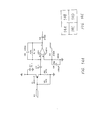
- Figure 10 shows a sensor configuration using many electrostatic radiators 21,22,23,24, driven by clock signals 0 1 , 0 2 , 4)3, 04 . and one electrostatic detector 3.
- This sensor configuration is capable of extracting one pixel of information per radiator less one, when inspecting a stationary object.
- This sensor configuration is described in further detail in the description of Figures 11 - 15.
- Figure 10 shows only one of many possible geometries in accordance with the present invention.
- sensor unit 58 includes a signal generating means 41 which drives a plurality of electrostatic radiators 42.
- An electrostatic field as produced by electrostatic radiators 42 is illustrated by broken lines 43.
- An electrostatic modifier 44 is shown within the field. It will be understood that lines 43 are merely illustrative, and are not intended to be an accurate portrayal of actual field lines (which, in any case, would be distorted depending on the actual configuration of modifier 44).
- electrostatic field that is formed, as modified by electrostatic modifier 44, is sensed by electrostatic detectors 45.
- the resulting signals are converted to a serial format by signal conditioning means 46, and are sent via serial link 57 to signal conversion means 47 which is implemented in computer 59.
- Computer 59 can be any suitable computer; for example, an AT-compatible with an EGA colour screen has been used. Computer 59 implements signal conversion means 47, and produces output image 48.
- FIG. 1 Not shown in Figure 1 is a serial link from computer 59 to sensor unit 58, with which computer 59 triggers each scan line to start.
- Sensor unit 58 starts a scan line upon receipt of any byte from computer 59.
- Scan lines consist of 8 data bytes sent in sequence. The description below of Figure 15 provides more detailed information.
- Signal conversion means 47 shall now be referred to by the term "software”.
- the software measures and displays a representation of surface profiles using data from signal conditioning means 46.
- An object to be sensed (not shown) is passed over the electrostatic radiators 42 through field 43, which is a near-field pattern.
- Each scan line is processed to yield a representation of a surface profile along one line, and an image is constructed from a series of scan lines, made as the object (not shown) passes the surface.
- the software implements the following functions: keyboard control, data file input and output, transmission of start bytes to sensor unit 58, receipt of 8 data bytes per scan line, offset removal, interpolation, integration, scaling, and display.
- a typical display as shown in Figure 16, consists of 30 scan lines, the scan line spacing being a function of object velocity and scan line frequency.
- Figure 16 is an output produced from a plastic package seal, where the seal could be seen physically as a depression of about 2 to 3 mm width, and 0.5 mm depth.
- the seal is viewed in cross- section.
- the package had a top surface with a metal layer embedded between two plastic layers, and was defect free.
- Figure 11 illustrates the implementation of sensor unit 58 in metal box 37 which provides electrostatic shielding and a mechanical reference for inspection of objects (not shown) placed on the top surface, in the electrostatic near field generated by the electrostatic radiators.
- the electrostatic radiators of extend upward to a small window (not shown), to lie flush with the top surface.
- An external 12 VDC power supply (not shown) is used to provide operating power.
- Figures 12 and 13 show the electrostatic radiators and detector used to obtain the output images shown in Figures 16 and 17.
- the electrostatic radiators and detector are mounted on two-sided printed circuit board 38, with 2-axis bevelled tongue 39 at the top, and hole 40 part-way down.
- the tongue has dimensions at the end of approximately 6 mm by 0.5 mm, and is used to support nine insulated solid wires of number 30 A.W.G. copper. These wires pass through hole 40 twice, having been looped around tongue 39 under tension, and are held in place by cyano-acrylate adhesive (not shown), covered by a thick layer of epoxy (not shown).
- the wires then are brought out in a group to signal generating means 41, contained in a programmable logic chip (EPLD) which produces clock signals 4)1 - ⁇ 9 .
- EPLD programmable logic chip
- One such suitable programmable logic is the EP900 made by Altera Corp of Santa Clara, California. This EPLD is a CMOS part, with accurate output voltage levels of 0 V and 5 V. A program listing for this part is given below at the end of this disclosure as Listing 7.
- circuit board 38 has FET buffer 60, to minimize loading of the small signal produced by detector electrode 3.
- This buffer contains a FET Q1, a bias resistor R5, one end of which is used as detector electrode 3, and a power supply filter capacitor C1.
- the buffer is interfaced to signal conditioning means 46 through two cables; one marked + 8 V for the FET drain, and a coaxial one marked COAX for the signal out (Vq), and a ground reference.
- Circuit board 38 is mounted so that wires 21 - 29 crossing the tip of the board are flush with the top surface of metal box 37, and detector electrode 3 is perpendicular to the wires, but parallel to the end of tongue 39 and to the top surface of the box.
- Metal box 37 acts like a Faraday shield, and helps to localize the sensing to the area just above the radiators and the detector. Rigid mounting of the electrostatic radiators and detector relative to the box is desirable to reduce unwanted signal variations caused by mechanical disturbance of field patterns.
- Signal generating means 41 is shown in further detail in Figure 15.
- U5 is a clock generator which oscillates at a frequency of 19,200 cycles per second, and directly drives U1, the EPLD.
- U1 divides the clock frequency by five, using a counter comprised of bits KO - K2, and then further divides the clock frequency by 256, using a counter comprised of bits CO -C7, where CO is the most frequently changing of these bits.
- the 256 states determined by CO - C7 are divided into eight groups of 32 states each, or 16 cycles of bit C0.
- Figures 14 and 15 show circuitry of signal generating means 41, buffer amplifier 5, and signal conditioning means 46.
- the CO - C7 bits are decoded to produce outputs PO - P8 from U1, corresponding to ⁇ 1 - ⁇ />9 respectively.
- Each group of 32 states corresponds to the application of bit CO to one of the ⁇ 1 - ⁇ 9 , and of the complement of CO to the next-higher-indexed clock signal ⁇ 1 - ⁇ 9 . In this way, a pair of adjacent clock signals are driven with opposite-phase clock levels, based on bit C0.
- CR is an output from the EPLD, provided as a reference clock for signal conditioning means 46.
- the clock PHI is level-shifted from the 5V logic levels of clock CR by inverters U4 to 8V logic levels.
- Figure 14 shows an electrostatic detector electrode E1 corresponding to detector electrode 3 in Figure 10, and FET buffer Q1 also in Figure 12 and corresponding to buffer amplifier 5 in Figure 10.
- circuits comprising part of signal conditions means 46. These include amplifier U2A, a synchronous detector comprising in part U1 and U2C and which uses clock PMI, offset removal potentiometers R9 - R16 which are selected through analog multiplexer U3 for individual pixel adjustment of signal Vq, and potentiometer R4 which with voltage buffer U2B is adjusted to keep the signal Vq within linear signal range.
- the output of amplifier U2A is approximately a square wave at the frequency of clock PHI, resulting from the signal at electrostatic detector electrode 3, or E1 in Figure 14, such signal being a sum of two terms of opposite phase, according to which pair of the clock signals ⁇ 1 - ⁇ 9 are currently driven.
- the output of amplifier U2A is level-shifted by capacitor C2 to yield a voltage such that the positive half-cycle of clock PHI corresponds to this voltage being equal to the reference output voltage from buffer amplifier U2B. During several negative half-cycles of clock PHI, this voltage is transferred to capacitor C4, and is further transferred during the positive half-cycles of clock PHI to capacitor C3. The voltage on capacitor C3 is amplified by amplifier U2C.
- Diode D1 shifts the output voltage. of amplifier U2C towards ground potential by approximately 0.6V, so that the output signal ANALOGIN has a low output voltage range to approximately ground potential.
- the signal at electrostatic detector element E1 is synchronously demodulated, and the output signal ANALOGIN settles to a DC value accordingly.
- Computer 59 sends a byte serially to start sensor unit 58, which then uses ⁇ 1 - ⁇ 9 , two at a time as described above, to obtain data for 8 points in sequence. These are converted to binary form, and transmitted serially to the computer as a sequence of 8 data bytes.
- the data link to the computer operates at 1200 baud.
- Serial interface to the computer is done by U3 and U4.
- U1 generates signals required to interface converter U2 to the serial link through integrated circuit U3, which comprises a full-duplex serial interface, known as a UART.
- Level shifting for the computer link is done by U4, which converts between RS 232-C levels required for the serial link and 5V logic levels required by U3.
- This listing contains information required to link together the various software modules used, in conjunction with sensor unit 58, to obtain the images of Figures 16 and 17.
- This listing contains the main program, which sets up global constants, memory allocation, and selects graphics mode. In addition, it displays on the screen a menu from which the operator selects various functions, such as autozero (F1 key), set inter-scan-line step size on the display (F5), set interpolation constant "k” (F6), acquire data (F7), save data buffer to disk file (F8), load disk file to data buffer and display data on the screen (F9), and exit from program (F10).
- autozero F1 key
- set inter-scan-line step size on the display F5
- set interpolation constant "k” F6
- acquire data F7
- save data buffer to disk file F8
- load disk file to data buffer and display data on the screen (F9)
- exit from program F10
- the "autozero_signal” removes DC offsets from the input data, first calling “acquire” to obtain raw data in a buffer, and then calling "autozero".
- the "change step” accepts a new constant, from the operator, for the vertical separation required between successive scan lines displayed.
- the "change_k” accepts a new constant k, from the operator, used during the pixel interpolation process.
- the value of k determines the overshoot and frequency response of the interpolation, which are inter-related. This constant is determined empirically, by selecting the k value yielding the best-looking display.
- the "acquire signal” polls the sensor unit for new data, and then displays the data. It calls “acquire” to obtain new data, “decimt” reduces the amount of data by accepting only one scan line of data per "D RATIO” scan lines, “offset_removal” makes use of the error values obtained by “autozero” to yield signals with little DC offset, “mean_of” finds the average value of the elements of the buffer and this value is assigned to the variable “dc”, “dc_removal” is used to ensure that when the signals are subsequently integrated they have the same end-points, “flip” reverses the polarity of the signal to be displayed so that more positive values will appear towards the top of the screen, “display - signal” does interpolation to give more points for the display and does filtering to smooth the traces and integrates the signals and then puts the output to the screen, “crt curpos” and “printf” are used to display the constant "dc” on the screen.
- the "save signal” calls “savebuf” to write the data buffer to a disk file.
- the "load_signal” calls “savebuf” to load the data buffer from a disk file.
- the "display_signal” calls “prof_format” which converts the data in “buff” to a 2-D array “prof ", “prof1 “_prof2” interpolates and integrates the data in the “prof1” “ array, and puts the result to “prof2", "prof1_prof3” is similar but integrates first and then interpolates to put results in "prof3", "disp profile” is called four times to give four different displays, namely the raw data, then two displays with steps shown between points, and finally a display with a smooth transition from one point to another using line interpolation. All four displays are shown on the screen at one time.
- the "drawscan” outputs points to the EGA screen according to an array of X-Y points provided.
- the "integrate” performs a discrete integration, or summation, over the input points.
- the "intp_flat" interpolates between points to provide new points to be displayed. This routine then interpolates again to yield steps on the display between the interpolated points. Note that two levels of interpolation are used here. The first level obtains extra points between pairs of the input points. The second level extends the first-level interpolated points sideways on the screen until a stair-case pattern is seen.
- intp line is similar to "intp flat", but in addition use line interpolation between the previously-interpolated points. This second level of interpolation fills in between the first-level interpolated points, by joining them on the screen using straight lines.
- intp fltr is similar to "intp_line”, but instead of line interpolation uses a low-pass filter for the second level of interpolation, resulting in a smoother display.
- interp_flat uses "intp flat", and is called by "display_profile”. "interp flat” sets up variables for "intp flat”, and calls in once per scan line of data to be displayed.
- interp_line uses “intp line” in a similar way.
- interp_filter uses “intp filter” in a similar way.
- Other routines in listing 3 set up the EGA graphics mode, and return to the normal mode.
- the "savebuf" writes the data buffer to a disk file.
- the "loadbuf” reads the data buffer from a disk file.
- the "getfile” opens a file specified by the operator, for read or write of a data buffer.
- the "no_echo_gets" reads a character string typed by the operator, without echoing a carriage return.
- the "printbottom” outputs a character string to line 24 on the screen.
- the "noechogetint” reads an integer typed by the operator, without echoing a carriage return.
- the "acquire" obtains new data from sensor unit 58.
- Serial port COM2 of computer 59 is used, with a data rate of 1200 baud.
- a byte is sent by computer 59 to port COM2.
- eight bytes from sensor unit 58 are read sequentially from COM2. This process is continued for several scan lines, equal in number to the variable "points".
- the “autozero” determines average values for each pixel element across the "points" scan lines in the buffer. These average values are found when no object 19 to be sensed is located near the sensor, and therefore represent error signals which are referred to as pixel offsets, and are stored for use by "offset removal".
- offset_removal takes the pixel offsets found by "autozero”, and subtracts them from the scan line data in the data buffer. Thus, the pixel errors are removed from all scan lines used for later display.
- the "dc_removal" is used to force the right ends of the integrated scan line data to have the value zero, the left ends being at zero automatically insofar as they precede the summation of the first actual data point. This is done by adding a DC value to the scan line data before integration. This procedure is appropriate for the plastic package seals, where it is known that the two ends of each scan must have the same value, and it is desirable to obtain a display with uniform end-points.
- the "ega_draw_pix” outputs a dot on the EGA screen, at specified coordinates x,y, where these values are scaled such that an increment of one corresponds to a shift of one pixel on the screen.
- the "crt_setcurpos” moves the cursor, used for character screen writing, to coordinates x,y, where these values are scaled such that an increment of one corresponds to a shift of one character on the screen.
- the "command” reads an undecoded key directly from the keyboard.
- Figures 18 - 21 show several sensor configurations using two electrostatic radiators 1, 2, and one electrostatic detector 3, producing output voltage Vq via amplifier 5.
- electrostatic detector electrode 3 is located above the electrostatic radiators 1,2 but nearby, and object 19 its perturbs of the electrostatic field patterns at the edge of the radiators 1,2.
- electrostatic radiators 1, 2 and electrostatic detector electrode 3 are coaxial, and object 19 is placed inside.
- the electrostatic radiators and electrostatic detector electrode are successive co-planar rings with detector 3 located between inner and outer radiators 1,2.
- Objects 19 is located above or below the plane.
- Figure 22 shows a sensor configuration using two electrostatic radiators 1,2, electrostatic detector electrodes 31, 32, 33, 34 and associated buffer amplifiers 51, 52, 53, 54. This sensor configuration is capable of extracting one pixel of information per detector electrode, when inspecting a stationary object.
- Figure 22 shows only one of many possible geometries in accordance with the present invention.
- Figure 23 shows a sensor configuration using several electrostatic radiators 21, 22, 23 and two electrostatic detector electrodes 31, 32. This sensor configuration is capable of extracting one pixel of information per detecting electrode, when inspecting a stationary object.
- Figure 23 shows only one possible geometry in accordance with the present invention.
- the line-scan sensor configuration in Figure 10 produces information about object 19 in the u direction. But relative motion in the v direction, of such a line-scan sensor configuration, yields a U-V array of data points. These points correspond to the quasi-gradient component parallel to the electrode axis.
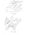
- Figure 24 shows a conceptual view of a sensor configuration capable of extracting an -approximation to the surface gradient of a face of object 19. This approximation to the surface gradient is referred to as the quasi-gradient, with respect to vectors u and v. In a scale drawing, the surface would be shown closer to the electrostatic radiators and detector. In this sensor configuration, charges q 1 and q 2 are used to extract the u term, and q 3 and q4 the v term, respectively. Only one pair of the orthogonally placed charges 1 and 2, or 17 and 18, may be non-zero at a time. In Figure 24, point 20, centered directly beneath electrostatic detector electrode 3, is the point about which information is being gathered.
- a quasi-gradient array may be obtained. From this, the surface may be calculated in a manner similar to that described in Figure 8, by non-linearly integrating the projection of the quasi-gradient along the line of the vector along which a cross-sectional surface profile is to be generated. A series of surface profiles can thus be generated, and then combined for a full 3-D map. A quasi-gradient projection along a line is calculated using a dot product, as is done in the calculation of a gradient projection along a line, which yields a slope.
- Figure 25 shows one method of obtaining the quasi-gradient array, from which surface profiles may be constructed.
- a sensor configuration with electrostatic radiators 21, 22, 23, 24, 25, 26, and electrostatic detector electrode 31 as in the sensor configuration in Figure 10 is mechanically moved past the object 19 in the u direction
- a second sensor configuration with electrostatic radiators 71, 72, 73, 74, 75, 76, and electrostatic detector electrode 32 is mechanically moved past the object in the v direction.
- Data from the two sensor configurations are combined to produce quasi-gradient vectors with u and v components.
- scanned part 20 of the surface of object 19. is shown, and an image may be constructed for this scanned part 20.
- Figure 26 shows a section of a sensor configuration with electrostatic radiators 21, 22, 23, 24, 25, 26, 27, 28, electrostatic detector electrode 3 and buffer amplifier 5, used to obtain both the u and v components when the external object (not shown) is moved past the sensor configuration in the u + v direction.
- Pairs of electrostatic radiators are selected for drive with opposite-phase clock signals as in Figure 10. For example, the pair ⁇ 5 and ⁇ 1>2 when so driven will yield a u component, and the pair ⁇ 6 and ⁇ 1 when so driven will yield a v component, with u and v as shown in Figure 26.
- the u and v axes are tilted at 45 to the direction of mechanical movement.
- Ground electrodes 61, 62, 63, 64 serve to control effects at the sensor ends, making the response for selected radiator pairs more uniform across the array than if the end electrodes were electrostatic radiators driven by signal generating means 41.
- Figure 27 is a conceptual view of X-Y sensor configuration 30, capable of individual pixel determination.of quasi-gradients. It can be seen as an extension of the two line scan sensor configurations in Figure 25 to cover all pixels at once, with electronic scanning of the array, and therefore not requiring the mechanical scanning of Figure 25. The axes are scanned sequentially rather than simultaneously, for the u and v components, to produce a quasi-gradient map.
- Figure 27 shows the various electrostatic detector electrodes connected to amplifiers 91 through 94 and 51 through 54. The four amplifiers 91 through 94 are connected to analog multiplexer 36 which provides an output signal Vqy about the quasi-gradient in the Y direction. Similarly, analog multiplexer 35 provides an output signal Vq x quasi-gradient in the X direction.
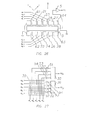
- Figure 28 shows an X-Y sensor configuration similar to that in Figure 27.
- a two-sided printed circuit board is used, with all electrostatic radiators and detectors located on one side, along with some of the interconnections, and with the remaining interconnections located on the other side.
- the electrostatic radiators and detector electrodes are connected as shown in Figure 29.
- Figure 29 is part of an X-Y sensor configuration as shown in Figure 28. It has a symmetric structure to avoid imbalance in the signal coupling to the electrostatic detector electrodes. Each electrostatic detector electrode has equal capacitive pickup from each pair of electrostatic radiators, when no external object is applied.
- Clock signal ⁇ 1y drives electrostatic radiators 21 a, 21 b, 21 which are equally spaced in the X direction
- clock signal ⁇ 2y drives radiators 22a, 22b, 22c also equally spaced in the X direction.
- spaced radiators are driven in the Y direction, where clock signal ⁇ 1x drives radiators 71a, 71b, and clock signal (A2x drives radiators 72a, 72b. Other radiators in the array are driven in a similar manner.
- the electrostatic detector electrodes are distributed regularly in the array. Detector electrodes 81 a and 81 b provide output signal V i y, and detector electrodes 82a and 82b provide output signal V 2 y, which are equally spaced in the X direction. Similarly spaced detector electrodes are located in the Y direction, such as detector electrodes 31a a and 31 b which produce output signal V ix .
- Figure 30 shows a sensor configuration, similar to that of Figure 10, but with electrostatic radiators 21 - 25 being formed with interleaved fingers. This serves to largely cancel the output signal Vq where two adjacent electrostatic radiators are driven in opposite phase, because the near-field pattern produced is reduced nearly to zero at the location of the object to be sensed (not shown).
- the interleaved fingers result in a fast-diminishing field with height when the fingers are differentially driven, but a slowly-diminishing field with height when the fingers are driven in phase. Therefore, it can be arranged that only when there are two adjacent sets of interleaved fingers driven in phase will there be a detectable signal.
- Figure 31 shows a sensor configuration using many electrostatic radiators 21 - 28 and one electrostatic detector electrode 3, wherein the electrostatic field shape and amplitude decay as a function of distance are programmed according to which radiators are driven. More distant electrostatic field patterns occur when opposite radiator pairs are activated than when are adjacent pairs. This has the effect of making the sensor configuration dynamically adjustable in terms of useful range. Opposite pairs can give guidance information in a vision application, and adjacent pairs can give more shape information around the ring. In this sensor configuration, the shape information. consists of 8 pixels. This permits distance and resolution to be optmized. In Figure 31 the central electrode 61 is connected to ground. Figure 31 shows only one of many possible geometries in accordance with the present invention.
- Figure 32 shows a sensor configuration using electrostatic radiators 21 and 22 and electrostatic detector electrode 3, wherein the radiating field geometry is different for each of the clock signals ⁇ 1 and q) 2 , with the result that the signal attenuation versus distance for the clock signals is different.
- the sensor configuration has a response which is a function of distance to the object (not shown), and can be used to determine distance when calibrated for known objects.
- Figure 33 shows a sensor configuration using electrostatic radiators 21a, 21 b, 21 c, 22a, 22b, 22c, 22d and electrostatic detector electrode 3, wherein the electrostatic field shape is controlled to produce a response which peaks along the center line.
- Two clock signals are used, with interdigitated radiators of empirically optimized geometries. Similar sensor configurations may be constructed using more clock . signals.
- Figure 34 shows a sensor configuration comprising two parallel rows of interdigitated pairs of electrostatic radiators 21, 22 and 23, 24, with electrostatic radiator 3 located between the rows.
- This sensor configuration may for example be used to obtain an average value for the depth of grooves on the surface of a metal object.
- the repeating pattern of the rows of radiators is aligned with these grooves, such that in each row the interdigitated pairs of electrostatic radiators have one set of radiators near the peaks, and one set of radiators near the valleys, determined with reference to the grooves.
- This function can be empirically determined, and sensor configuration output Vq can then be compensated, resulting in a measurement of the depth of the grooves, averaged over all grooves near the electrostatic radiators and detector.
- Measurement of the depth of the grooves requires that the object to be sensed (not shown) be centered detector electrode 3.
- the pairs of clock signals 4 ) 1 , (P2 and 4 ) 3 , 04 are driven with the same polarity for each clock in the pair but with the pairs themselves having opposite clock polarity, resulting in a temporary sensor configuration such as that in Figure 2.
- the detector will produce a signal when the cylinder is nearby, but not centered on detector electrode 3.
- the cylinder is assumed to be passing by the sensor configuration.
- the output signal Vq crosses zero, the external object is at that time approximately centered.
- the sensor mode is changed to permit measurement of groove depth.
- Figure 35 shows a sensor configuration comprising two parallel rows of interdigitated pairs of electrostatic radiators 21, 22 and 23, 24 with electrostatic detector electrode 3 located between the rows. Operation is similar to the sensor configuration in Figure 34. However, the rows are offset by one half the inter-radiator spacing, to produce contributions to the electrostatic field which overlap. The overlap of these fields permits an approximate determination of the relative vertical position of the radiators and, for example, a cylinder with grooves (not shown). The vertical position is not determined uniquely in terms of integer multiples of groove height. As an example of approximate height determination, the signals from the two rows of radiators can be analyzed in terms of phase quadrature to each other. The phase angle is then used to assist in the compensation of the sensor. This compensation may be done based on empirically determined data. The calculation of phase angle is not accurate, due to the non-linear nature of the component signals involved. However, this may be unimportant when the phase angle is used only as a signal used to weight the contributions of the two rows of radiators in the final groove depth calculations.
- Electrostatic radiator and electrostatic detector electrode geometry can have significant effects on the signal produced, and may require optimization for a particular application. Those shown are in accordance with the present invention, but do not limit its scope.
Applications Claiming Priority (2)
| Application Number | Priority Date | Filing Date | Title |
|---|---|---|---|
| CA614905 | 1989-09-29 | ||
| CA614905 | 1989-09-29 |
Publications (1)
| Publication Number | Publication Date |
|---|---|
| EP0425823A1 true EP0425823A1 (de) | 1991-05-08 |
Family
ID=4140844
Family Applications (1)
| Application Number | Title | Priority Date | Filing Date |
|---|---|---|---|
| EP90118729A Withdrawn EP0425823A1 (de) | 1989-09-29 | 1990-09-28 | Elektrostatische Abbildungsvorrichtung |
Country Status (2)
| Country | Link |
|---|---|
| US (1) | US5430381A (de) |
| EP (1) | EP0425823A1 (de) |
Cited By (5)
| Publication number | Priority date | Publication date | Assignee | Title |
|---|---|---|---|---|
| WO1992006351A1 (en) * | 1990-10-03 | 1992-04-16 | Renishaw Plc | Capacitance sensing probe |
| WO1992008947A1 (en) * | 1990-11-16 | 1992-05-29 | Moonstone Designs Limited | Device for determining the presence and/or characteristics of an object or a substance |
| EP0556682A1 (de) * | 1992-02-10 | 1993-08-25 | SYEL di FRANCHI A.- MARTOLINI A. & C. s.n.c. | Sensorstangenvorrichtung zur Feststellung der Form und der Annäherung von Gegenständen aus verschiedenem Stoffen |
| WO1996014554A1 (en) * | 1994-11-07 | 1996-05-17 | British Nuclear Fuels Plc | A transducer |
| FR2738910A1 (fr) * | 1995-09-15 | 1997-03-21 | Superba Sa | Capteur de mouvements dans l'espace, en particulier pour la mesure sans contact des caracteristiques d'un produit lineaire ou surfacique |
Families Citing this family (35)
| Publication number | Priority date | Publication date | Assignee | Title |
|---|---|---|---|---|
| EP0790479B1 (de) | 1996-02-14 | 2002-01-16 | STMicroelectronics S.r.l. | Kapazitiver Abstandssensor, insbesondere zur Erfassung von Fingerabdrücken |
| US6114862A (en) * | 1996-02-14 | 2000-09-05 | Stmicroelectronics, Inc. | Capacitive distance sensor |
| US6320394B1 (en) | 1996-02-14 | 2001-11-20 | Stmicroelectronics S.R.L. | Capacitive distance sensor |
| US6078179A (en) * | 1997-04-24 | 2000-06-20 | Dkl International, Inc. | Selective polarization matching filter for triggering and maximizing rapid dielectrokinesis response |
| US6483931B2 (en) | 1997-09-11 | 2002-11-19 | Stmicroelectronics, Inc. | Electrostatic discharge protection of a capacitve type fingerprint sensing array |
| US6191593B1 (en) | 1997-12-17 | 2001-02-20 | Stmicroelectronics, Inc. | Method for the non-invasive sensing of physical matter on the detection surface of a capacitive sensor |
| SE511543C2 (sv) * | 1998-02-16 | 1999-10-18 | Fingerprint Cards Ab | Anordning och metod för kapacitiv avkänning av topologiska variationer |
| US6091082A (en) | 1998-02-17 | 2000-07-18 | Stmicroelectronics, Inc. | Electrostatic discharge protection for integrated circuit sensor passivation |
| US6431678B2 (en) * | 1998-09-01 | 2002-08-13 | Hewlett-Packard Company | Ink leakage detecting apparatus |
| US6512381B2 (en) | 1999-12-30 | 2003-01-28 | Stmicroelectronics, Inc. | Enhanced fingerprint detection |
| US7239227B1 (en) | 1999-12-30 | 2007-07-03 | Upek, Inc. | Command interface using fingerprint sensor input system |
| US6943665B2 (en) | 2000-03-21 | 2005-09-13 | T. Eric Chornenky | Human machine interface |
| US20030098774A1 (en) * | 2000-03-21 | 2003-05-29 | Chornenky Todd E. | Security apparatus |
| US6429666B1 (en) * | 2000-04-17 | 2002-08-06 | Sentronics Corporation | Capacitive circuit array for fingerprint sensing |
| IT1318487B1 (it) * | 2000-04-21 | 2003-08-25 | Ausimont Spa | Fluoroelastomeri. |
| US7534845B2 (en) | 2000-04-21 | 2009-05-19 | Solvay Solexis S.P.A. | Fluorovinyl ethers and polymers obtainable therefrom |
| IT1318488B1 (it) * | 2000-04-21 | 2003-08-25 | Ausimont Spa | Fluorovinileteri e polimeri da essi ottenibili. |
| US6864687B2 (en) * | 2001-08-01 | 2005-03-08 | Amfit, Inc. | Electrostatic sensor device and matrix |
| ITMI20012164A1 (it) * | 2001-10-18 | 2003-04-18 | Ausimont Spa | Fluoroelastomeri |
| FR2844349B1 (fr) * | 2002-09-06 | 2005-06-24 | Nanotec Solution | Detecteur de proximite par capteur capacitif |
| US7330032B2 (en) * | 2003-12-30 | 2008-02-12 | The Mitre Corporation | Techniques for building-scale electrostatic tomography |
| US7126356B2 (en) * | 2004-04-30 | 2006-10-24 | Intel Corporation | Radiation detector for electrostatic discharge |
| US8115497B2 (en) * | 2007-11-13 | 2012-02-14 | Authentec, Inc. | Pixel sensing circuit with common mode cancellation |
| US8378689B2 (en) * | 2009-07-14 | 2013-02-19 | Amfit, Inc | Electrostatic sensor device and matrix |
| US9279719B2 (en) * | 2011-02-03 | 2016-03-08 | The United States Of America As Represented By The Administrator Of The National Aeronautics And Space Administration | Electric field quantitative measurement system and method |
| DE102011078369B4 (de) * | 2011-06-29 | 2013-02-28 | Ident Technology Ag | Kapazitive Sensoreinrichtung sowie Verfahren zum Kalibrieren einer kapazitiven Sensoreinrichtung |
| US9322794B2 (en) * | 2012-12-18 | 2016-04-26 | Apple Inc. | Biometric finger sensor including array shielding electrode and related methods |
| US11307235B2 (en) | 2012-12-28 | 2022-04-19 | Illinois Tool Works Inc. | In-tool ESD events selective monitoring method and apparatus |
| US9671448B2 (en) | 2012-12-28 | 2017-06-06 | Illinois Tool Works Inc. | In-tool ESD events monitoring method and apparatus |
| US9804199B2 (en) | 2013-11-19 | 2017-10-31 | The United States of America as Represented by NASA | Ephemeral electric potential and electric field sensor |
| US10024900B2 (en) | 2016-06-09 | 2018-07-17 | United States Of America As Represented By The Administrator Of Nasa. | Solid state ephemeral electric potential and electric field sensor |
| US10712378B2 (en) | 2016-07-01 | 2020-07-14 | United States Of America As Represented By The Administrator Of Nasa | Dynamic multidimensional electric potential and electric field quantitative measurement system and method |
| US10900930B2 (en) | 2016-07-15 | 2021-01-26 | United States Of America As Represented By The Administrator Of Nasa | Method for phonon assisted creation and annihilation of subsurface electric dipoles |
| US10281430B2 (en) | 2016-07-15 | 2019-05-07 | The United States of America as represented by the Administratior of NASA | Identification and characterization of remote objects by electric charge tunneling, injection, and induction, and an erasable organic molecular memory |
| US10620252B2 (en) | 2017-01-19 | 2020-04-14 | United States Of America As Represented By The Administrator Of Nasa | Electric field imaging system |
Citations (4)
| Publication number | Priority date | Publication date | Assignee | Title |
|---|---|---|---|---|
| EP0004757A1 (de) * | 1978-03-31 | 1979-10-17 | Gould Inc. | Kapazitives berührungsfreies Messystem |
| DE2851742A1 (de) * | 1978-11-30 | 1980-06-19 | Gewerk Eisenhuette Westfalia | Vortriebsschild mit darin verlagerter vortriebsmaschine |
| EP0067643A2 (de) * | 1981-06-12 | 1982-12-22 | Peter Caleb Frederick Wolfendale | Verfahren zur Feststellung der Dimensionen und/oder der Gestalt von Oberflächen |
| WO1988001747A1 (en) * | 1986-09-03 | 1988-03-10 | Extrude Hone Corporation | Capacitor array sensors tactile and proximity sensing and methods of use thereof |
Family Cites Families (14)
| Publication number | Priority date | Publication date | Assignee | Title |
|---|---|---|---|---|
| NL271951A (de) * | 1961-07-25 | |||
| DE2529475C3 (de) * | 1975-07-02 | 1981-10-08 | Ewald Max Christian Dipl.-Phys. 6000 Frankfurt Hennig | Elektrische Schaltungsanordnung zum zeitabhängigen Messen von physikalischen Größen |
| US4082990A (en) * | 1976-09-29 | 1978-04-04 | The Singer Company | Electrostatic pickoff and torquer |
| US4112355A (en) * | 1976-10-22 | 1978-09-05 | Lockheed Corporation | Quality and fit measuring apparatus for fasteners and their holes |
| SU844986A1 (ru) * | 1979-08-02 | 1981-07-07 | Предприятие П/Я Г-4708 | Емкостный преобразователь |
| JPS5759101A (en) * | 1980-09-26 | 1982-04-09 | Hiromi Ogasawara | Noncontacting infinitesimal displacement gauge |
| FR2519137A1 (fr) * | 1981-12-24 | 1983-07-01 | Europ Agence Spatiale | Detecteur de position a deux axes pour dispositif a suspension magnetique |
| US4686531A (en) * | 1983-10-28 | 1987-08-11 | Control Data Corporation | Capacitance height gage applied in reticle position detection system for electron beam lithography apparatus |
| US4814691A (en) * | 1985-08-09 | 1989-03-21 | Washington Research Foundation | Fringe field capacitive sensor for measuring profile of a surface |
| GB2214640B (en) * | 1988-01-20 | 1992-05-20 | Univ Manchester | Tomographic flow imaging system |
| US4899101A (en) * | 1988-01-21 | 1990-02-06 | The United States Of America As Represented By The United States Department Of Energy | Online capacitive densitometer |
| US4972154A (en) * | 1989-06-06 | 1990-11-20 | Metriguard, Inc | Apparatus and method for measuring wood grain angle |
| US5281921A (en) * | 1990-04-24 | 1994-01-25 | Novak James L | Non-contact capacitance based image sensing method and system |
| US5363051A (en) * | 1992-11-23 | 1994-11-08 | The United States Of America As Represented By The Administrator Of The National Aeronautics And Space Administration | Steering capaciflector sensor |
-
1990
- 1990-09-28 EP EP90118729A patent/EP0425823A1/de not_active Withdrawn
-
1993
- 1993-10-04 US US08/131,497 patent/US5430381A/en not_active Expired - Fee Related
Patent Citations (4)
| Publication number | Priority date | Publication date | Assignee | Title |
|---|---|---|---|---|
| EP0004757A1 (de) * | 1978-03-31 | 1979-10-17 | Gould Inc. | Kapazitives berührungsfreies Messystem |
| DE2851742A1 (de) * | 1978-11-30 | 1980-06-19 | Gewerk Eisenhuette Westfalia | Vortriebsschild mit darin verlagerter vortriebsmaschine |
| EP0067643A2 (de) * | 1981-06-12 | 1982-12-22 | Peter Caleb Frederick Wolfendale | Verfahren zur Feststellung der Dimensionen und/oder der Gestalt von Oberflächen |
| WO1988001747A1 (en) * | 1986-09-03 | 1988-03-10 | Extrude Hone Corporation | Capacitor array sensors tactile and proximity sensing and methods of use thereof |
Cited By (8)
| Publication number | Priority date | Publication date | Assignee | Title |
|---|---|---|---|---|
| WO1992006351A1 (en) * | 1990-10-03 | 1992-04-16 | Renishaw Plc | Capacitance sensing probe |
| US5270664A (en) * | 1990-10-03 | 1993-12-14 | Renishaw, Plc | Probe for measuring surface roughness by sensing fringe field capacitance effects |
| WO1992008947A1 (en) * | 1990-11-16 | 1992-05-29 | Moonstone Designs Limited | Device for determining the presence and/or characteristics of an object or a substance |
| GB2265720A (en) * | 1990-11-16 | 1993-10-06 | Moonstone Designs Ltd | Device for determining the presence and /or characteristics of an object or a substance |
| GB2265720B (en) * | 1990-11-16 | 1995-06-14 | Moonstone Designs Ltd | Device for determining the presence and/or characteristics of an object or a substance |
| EP0556682A1 (de) * | 1992-02-10 | 1993-08-25 | SYEL di FRANCHI A.- MARTOLINI A. & C. s.n.c. | Sensorstangenvorrichtung zur Feststellung der Form und der Annäherung von Gegenständen aus verschiedenem Stoffen |
| WO1996014554A1 (en) * | 1994-11-07 | 1996-05-17 | British Nuclear Fuels Plc | A transducer |
| FR2738910A1 (fr) * | 1995-09-15 | 1997-03-21 | Superba Sa | Capteur de mouvements dans l'espace, en particulier pour la mesure sans contact des caracteristiques d'un produit lineaire ou surfacique |
Also Published As
| Publication number | Publication date |
|---|---|
| US5430381A (en) | 1995-07-04 |
Similar Documents
| Publication | Publication Date | Title |
|---|---|---|
| US5430381A (en) | Apparatus for electrostatically imaging the surface of an object located nearby | |
| Tanner et al. | An integrated analog optical motion sensor | |
| US5376948A (en) | Method of and apparatus for touch-input computer and related display employing touch force location external to the display | |
| US4503922A (en) | Electronic bathroom scale apparatus using planar coil sensors | |
| US5304937A (en) | Capacitive position sensor with an electrode array cursor and topographically featured scale | |
| US5373245A (en) | Capaciflector camera | |
| EP0326266B1 (de) | Tomografisches Abbildungssystem für Strömungsfelder | |
| US5790107A (en) | Touch sensing method and apparatus | |
| US5650844A (en) | LCD panel image quality inspection system and LCD image presampling method | |
| EP0277964B1 (de) | Optische abtastvorrichtung mit ortungsfühlern | |
| US5198623A (en) | Method for use in a digitizer for determining pen tilt | |
| US4841225A (en) | Capacitive sensor for measuring a displacement | |
| CN102498368A (zh) | 包括光学应变仪的远程位移传感器的装置及其系统 | |
| US20040120603A1 (en) | Enhancing the resolution of measurement systems employing image capturing systems to measure lengths | |
| US5013154A (en) | System for remotely reading an analog meter | |
| US5717782A (en) | Method and apparatus for restoring digitized video pictures generated by an optical surface-height profiler | |
| JPH0544963B2 (de) | ||
| Li et al. | An accurate low-cost capacitive absolute angular-position sensor with a full-circle range | |
| US5287105A (en) | Automatic tracking and scanning cursor for digitizers | |
| US5101081A (en) | Graphics surface assembly with calibrating memory device | |
| CN100536785C (zh) | 一种数字扫描变换器实现方法 | |
| JPH0115085B2 (de) | ||
| CN100536786C (zh) | 一种超声图像反转显示的方法 | |
| Field et al. | Capacitive position sensor with simultaneous, linear X–Y readout | |
| CN100536787C (zh) | 一种按比例显示超声图像的方法 |
Legal Events
| Date | Code | Title | Description |
|---|---|---|---|
| PUAI | Public reference made under article 153(3) epc to a published international application that has entered the european phase |
Free format text: ORIGINAL CODE: 0009012 |
|
| AK | Designated contracting states |
Kind code of ref document: A1 Designated state(s): AT BE CH DE DK ES FR GB GR IT LI LU NL SE |
|
| 17P | Request for examination filed |
Effective date: 19911108 |
|
| RAP1 | Party data changed (applicant data changed or rights of an application transferred) |
Owner name: ANTIVISION SYSTEMS CORP. |
|
| 17Q | First examination report despatched |
Effective date: 19930222 |
|
| STAA | Information on the status of an ep patent application or granted ep patent |
Free format text: STATUS: THE APPLICATION IS DEEMED TO BE WITHDRAWN |
|
| 18D | Application deemed to be withdrawn |
Effective date: 19950124 |