EP0425739A1 - Alignment apparatus and SOR X-ray exposure apparatus having same - Google Patents
Alignment apparatus and SOR X-ray exposure apparatus having same Download PDFInfo
- Publication number
- EP0425739A1 EP0425739A1 EP89311195A EP89311195A EP0425739A1 EP 0425739 A1 EP0425739 A1 EP 0425739A1 EP 89311195 A EP89311195 A EP 89311195A EP 89311195 A EP89311195 A EP 89311195A EP 0425739 A1 EP0425739 A1 EP 0425739A1
- Authority
- EP
- European Patent Office
- Prior art keywords
- mask
- wafer
- stage
- ray
- exposure
- Prior art date
- Legal status (The legal status is an assumption and is not a legal conclusion. Google has not performed a legal analysis and makes no representation as to the accuracy of the status listed.)
- Granted
Links
Images


Classifications
-
- G—PHYSICS
- G03—PHOTOGRAPHY; CINEMATOGRAPHY; ANALOGOUS TECHNIQUES USING WAVES OTHER THAN OPTICAL WAVES; ELECTROGRAPHY; HOLOGRAPHY
- G03F—PHOTOMECHANICAL PRODUCTION OF TEXTURED OR PATTERNED SURFACES, e.g. FOR PRINTING, FOR PROCESSING OF SEMICONDUCTOR DEVICES; MATERIALS THEREFOR; ORIGINALS THEREFOR; APPARATUS SPECIALLY ADAPTED THEREFOR
- G03F9/00—Registration or positioning of originals, masks, frames, photographic sheets or textured or patterned surfaces, e.g. automatically
- G03F9/70—Registration or positioning of originals, masks, frames, photographic sheets or textured or patterned surfaces, e.g. automatically for microlithography
- G03F9/7088—Alignment mark detection, e.g. TTR, TTL, off-axis detection, array detector, video detection
-
- G—PHYSICS
- G03—PHOTOGRAPHY; CINEMATOGRAPHY; ANALOGOUS TECHNIQUES USING WAVES OTHER THAN OPTICAL WAVES; ELECTROGRAPHY; HOLOGRAPHY
- G03F—PHOTOMECHANICAL PRODUCTION OF TEXTURED OR PATTERNED SURFACES, e.g. FOR PRINTING, FOR PROCESSING OF SEMICONDUCTOR DEVICES; MATERIALS THEREFOR; ORIGINALS THEREFOR; APPARATUS SPECIALLY ADAPTED THEREFOR
- G03F7/00—Photomechanical, e.g. photolithographic, production of textured or patterned surfaces, e.g. printing surfaces; Materials therefor, e.g. comprising photoresists; Apparatus specially adapted therefor
- G03F7/70—Microphotolithographic exposure; Apparatus therefor
- G03F7/70008—Production of exposure light, i.e. light sources
-
- G—PHYSICS
- G03—PHOTOGRAPHY; CINEMATOGRAPHY; ANALOGOUS TECHNIQUES USING WAVES OTHER THAN OPTICAL WAVES; ELECTROGRAPHY; HOLOGRAPHY
- G03F—PHOTOMECHANICAL PRODUCTION OF TEXTURED OR PATTERNED SURFACES, e.g. FOR PRINTING, FOR PROCESSING OF SEMICONDUCTOR DEVICES; MATERIALS THEREFOR; ORIGINALS THEREFOR; APPARATUS SPECIALLY ADAPTED THEREFOR
- G03F7/00—Photomechanical, e.g. photolithographic, production of textured or patterned surfaces, e.g. printing surfaces; Materials therefor, e.g. comprising photoresists; Apparatus specially adapted therefor
- G03F7/70—Microphotolithographic exposure; Apparatus therefor
- G03F7/70058—Mask illumination systems
- G03F7/702—Reflective illumination, i.e. reflective optical elements other than folding mirrors, e.g. extreme ultraviolet [EUV] illumination systems
-
- G—PHYSICS
- G03—PHOTOGRAPHY; CINEMATOGRAPHY; ANALOGOUS TECHNIQUES USING WAVES OTHER THAN OPTICAL WAVES; ELECTROGRAPHY; HOLOGRAPHY
- G03F—PHOTOMECHANICAL PRODUCTION OF TEXTURED OR PATTERNED SURFACES, e.g. FOR PRINTING, FOR PROCESSING OF SEMICONDUCTOR DEVICES; MATERIALS THEREFOR; ORIGINALS THEREFOR; APPARATUS SPECIALLY ADAPTED THEREFOR
- G03F7/00—Photomechanical, e.g. photolithographic, production of textured or patterned surfaces, e.g. printing surfaces; Materials therefor, e.g. comprising photoresists; Apparatus specially adapted therefor
- G03F7/70—Microphotolithographic exposure; Apparatus therefor
- G03F7/70691—Handling of masks or workpieces
-
- G—PHYSICS
- G03—PHOTOGRAPHY; CINEMATOGRAPHY; ANALOGOUS TECHNIQUES USING WAVES OTHER THAN OPTICAL WAVES; ELECTROGRAPHY; HOLOGRAPHY
- G03F—PHOTOMECHANICAL PRODUCTION OF TEXTURED OR PATTERNED SURFACES, e.g. FOR PRINTING, FOR PROCESSING OF SEMICONDUCTOR DEVICES; MATERIALS THEREFOR; ORIGINALS THEREFOR; APPARATUS SPECIALLY ADAPTED THEREFOR
- G03F7/00—Photomechanical, e.g. photolithographic, production of textured or patterned surfaces, e.g. printing surfaces; Materials therefor, e.g. comprising photoresists; Apparatus specially adapted therefor
- G03F7/70—Microphotolithographic exposure; Apparatus therefor
- G03F7/708—Construction of apparatus, e.g. environment aspects, hygiene aspects or materials
- G03F7/70808—Construction details, e.g. housing, load-lock, seals or windows for passing light in or out of apparatus
- G03F7/70841—Constructional issues related to vacuum environment, e.g. load-lock chamber
-
- G—PHYSICS
- G03—PHOTOGRAPHY; CINEMATOGRAPHY; ANALOGOUS TECHNIQUES USING WAVES OTHER THAN OPTICAL WAVES; ELECTROGRAPHY; HOLOGRAPHY
- G03F—PHOTOMECHANICAL PRODUCTION OF TEXTURED OR PATTERNED SURFACES, e.g. FOR PRINTING, FOR PROCESSING OF SEMICONDUCTOR DEVICES; MATERIALS THEREFOR; ORIGINALS THEREFOR; APPARATUS SPECIALLY ADAPTED THEREFOR
- G03F7/00—Photomechanical, e.g. photolithographic, production of textured or patterned surfaces, e.g. printing surfaces; Materials therefor, e.g. comprising photoresists; Apparatus specially adapted therefor
- G03F7/70—Microphotolithographic exposure; Apparatus therefor
- G03F7/708—Construction of apparatus, e.g. environment aspects, hygiene aspects or materials
- G03F7/70858—Environment aspects, e.g. pressure of beam-path gas, temperature
- G03F7/70866—Environment aspects, e.g. pressure of beam-path gas, temperature of mask or workpiece
-
- G—PHYSICS
- G03—PHOTOGRAPHY; CINEMATOGRAPHY; ANALOGOUS TECHNIQUES USING WAVES OTHER THAN OPTICAL WAVES; ELECTROGRAPHY; HOLOGRAPHY
- G03F—PHOTOMECHANICAL PRODUCTION OF TEXTURED OR PATTERNED SURFACES, e.g. FOR PRINTING, FOR PROCESSING OF SEMICONDUCTOR DEVICES; MATERIALS THEREFOR; ORIGINALS THEREFOR; APPARATUS SPECIALLY ADAPTED THEREFOR
- G03F9/00—Registration or positioning of originals, masks, frames, photographic sheets or textured or patterned surfaces, e.g. automatically
- G03F9/70—Registration or positioning of originals, masks, frames, photographic sheets or textured or patterned surfaces, e.g. automatically for microlithography
- G03F9/7049—Technique, e.g. interferometric
Definitions
- the exposure unit 102 is required to be aligned in the six axes similarly to the case of the mirror unit 101, relative to the SOR optical axes of the SOR ring 4 and the mirror unit 101.
- a fluid bearing is provided at the bottom of the unit so as to make easier movement of the exposure unit 102 in X and Z directions and the rotation ( ⁇ y) about the Y axis.
- the rotational motion ( ⁇ x, ⁇ ) about X and Z axes and the motion in the Y direction are effected by controlling pressure of the air suspension 8402, 8403 and 8404 shown in Figure 84.
- a wafer traverser 1306 functions mainly to convey the wafer 3 from the orientation flat detecting stage 1305 to the stage 1301 and in the opposite direction.
- the wafer traverser 1306 moves in the Z direction on the orientation flat detecting stage 1305 and at the wafer transferring position of the stage 1301 and also moves in the X direction from the orientation flat detecting stage 1305.
- a plurality of wafer hands are provided to supply and take up the wafers, exclusively. They are moved in the opposite directions along the X axis.
- Each hand of the wafer traverser 1306 is required to stop at a predetermined position on the stage 1301, and therefore, it is directly mounted to a member of the stage 1301.
- the heat generating parts such as a driving actuator or the like is supplied with the constant temperature fluid so as to prevent the temperature change thereof.
- An injector 1304 has a main functions to dispense the wafer 3 from and accommodate it into a wafer carrier of a wafer supply and take up apparatus 1303 and to supply the wafer 3 to or remove it from the orientation flat detecting stage 1305.
- the injector 1304 is capable of moving a wafer supporting surface of a wafer hand between horizontal position and vertical position, and the hand is movable in the X (or Z) direction, and is movable about the Y axis.
- the injector 1304 is mounted to the wall of the chamber 3101.
- the heat generating elements of the injection 1304 is supplied with a constant temperature water to prevent the temperature change.
- the shape of the stage apparatus 1301 is such that it is longer in the Y direction, and the measurement optical system 1312 is disposed on the top surface of the frame 1701 ( Figure 17) in the Y direction.
- the transfer position is disposed topmost possible position in the Figure. With those arrangement, the number of movable parts above the mask 2 and the wafer 3 is reduced, so that the problem of contamination falling is eliminated. Also, the mask conveying apparatus 1311, the orientation flat detecting stage 1305, the injector 1304, the wafer traverser 1305 or the like are necessarily disposed at a lower side in the Figure of the transfer position, and therefore, the transfer position is protected from the dust produced by those subunits.
- the vacuum chamber 1408 and the frame 1407 are independently fixed to an unshown base, and therefore, the deformation of the vacuum chamber 1408 attributable to the changes in the temperature for the ambient pressure does not influence the pose or position of the X-ray mirror 1401. Therefore, the rigidity of the vacuum chamber 1408 can be decreased to permit reduction of the weight.
- a discharge port 1411 is connected with a discharge pump 1412 for maintaining a high vacuum in the vacuum chamber 1408.
- a shutter 1409 is provided to avoid that the X-ray mirror 1401 receives the SOR rays when it is not necessary, by which the time period during which the X-ray mirror 1401 is dozed with the SOR rays. The reduction of the time period is contributable to reduce the damage of the X-ray mirror 1401 by the radiation.
- the steel belt 1517 is stretched between the driving drum 1515 driven by the actuator unit 1518 and the idler drum 1516, and the inside of the steel belt 1515 is driven by the driving drum 1515 through friction.
- the driving drum 1515 is crowned by which the central portion of the drum has a larger diameter than that of the marginal portions by 50 - 100 microns so as to stabilize the movement of the steel belt 1517 without rolling. Adjacent opposite ends of the steel belt 1517, a small rectangular openings are formed, one of which is a timing aperture 1534, and the other of which is a position detecting aperture 1535.
- An X-ray detector is mounted to the fine movement stage 1804 ( Figure 18) when the two shutter units 1501 and 1502 are maintained opened, and a Y coarse movement stage 1705 ( Figure 17) is driven to scanningly move in the Y direction in the exposure area the X-ray detector 1511, the strength profile of the X-ray can be measured.
- a driving table for driving the actuator unit 1514 is produced, and the correcting drive to provide the constant energy absorption of the resist in the exposure area can be effected.
- the actuator units 2415 and 2416 in the ⁇ and ⁇ directions are hermetically sealed by an aluminum alloy casing enclosing a DC motor, a rotary encoder and a reduction mechanism, and similarly to the actuator unit for the exposure shut apparatus 1308, the heat generated by the motor and the reduction mechanism is carried over outside the chamber through an unshown pipes.
- the axis of the pattern on the mask 2 is directly aligned with the movement direction of the reference mark representing the coordinate axis of the stage apparatus 1301 ruling the column and line direction of the patterns, and therefore, the mask alignment is very precise.
- the adjustment is required to mechanically align with high precision the line defined by the two points to the coordinate axis of the stage apparatus 1301.
- such an adjustment is not necessary when the reference marks 1821 which are functionally deemed as one point are mounted on the laser distance measuring mirror 1810. This is particularly advantageous in the easy servicing operation in the field.
- a mask chamber 3103 is connected through a mask gate valve 3102 which will hereinafter be called also "MKGV".
- the shutter chamber 3104 accommodates the exposure shutter apparatus 1308, and to the chamber 3104 an X-ray mirror port 3105 is conencted through the Be window 3512.
- the prealignment system 1307 is accommodated in the automatic prealignment chamber 3106.
- the mask chamber 3103 contains the mask cassette loader 1309 with the exception of the elevator driving unit 2805 and the indexer.
- a wafer traverser 1304 is accommodated except X, ⁇ y driving units 2516 and 2515.
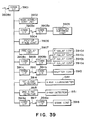
- Figure 40 shows the structures of the fine automatic alignment and automatic focusing controlling sections 3910a - 3910d, in which the elements shown in Figure 23 are omitted.
- a communication path 3909 for communication with the main assembly controlling unit 3902 shown in Figure 39
- a communication interface 3908b for reception of instructions through the communication path 3909 and transmission of alignment information and gap information
- fine alignment and focusing interface 4004 for receiving instructions from the communication interface 3908b, producing signals for alignment measurement and gap measurement and transmitting the alignment information and the gap information to the communication interface 3908b.
- a fine alignment and focusing laser diode driver 4001 drives the semiconductor laser 2301 by the light output determined by the fine alignment and focusing interface 4004.
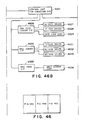
- the ⁇ axis drivers 4206a - 4206d and ⁇ axis drivers 4207a - 4207d are driver, for DC motors, and it is possible that in response to the instructions from the main control unit 3902, its servo loop is shut off.
- the pickup head cramp controlling section 4205 includes a driver 4208 for an actuator for pressing the pickup device 2401 to the pickup reference surfaces 2401 in order to reduce the position control error by pitching and rolling of the pickup device 2401, and a sensor 4209 for confirming the pressing.
- only one electromagnetic valve (not shown) for a compressed air operable to press the pickups 2401 is provided for four pickup stages 2411.
- the sensor (not shown) for confirmation of the pressed state is provided for each of the pickup stages, and therefore the sensor 4209 is provided with four channel inputs.
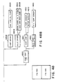
- the pressure gauge input portion 4805 receives the sensor output from the mirror port pressure gauge 3519 for measuring the pressure of the mirror port 3105 and a sensor output from the main chamber pressure gauge 3510 for measuring the pressure of the main chamber 3101, and it processes the outputs and transmits the data to the supply and discharge interface 4803.
- the vacuum pump driver 4806 is used commonly for the main chamber 3101, the wafer loading sub-chamber 3109, the wafer unloading sub-chamber 3111 and the mask sub-chamber 3103. It also on-off controls the coarse discharge oil rotation pump 3303 and the main discharge oil rotation pump 3307 and drives and monitors the state of operation of the main discharge turbo molecule pump 3306.
- the mask cassette taking out instructions are to execute the process for taking the mask cassette set into the apparatus by the operator to establish an exchangeable conditions.
- the discrimination is made at step 4917 as to whether or not a mask cassette is currently set, and whether or not the conditions for execution of the mask cassette taking out processing are satisfied. If so, at step 4918 the mask cassette taking out process is executed. Then, the mask cassette 1310 can be taken out, and the sequence goes back to the step 4913.
- the X-ray strength profile measurement instructions (step 4922) is to execute the process for producing shutter driving data for assuring uniform X-ray exposure amount over the entire exposure area against change in the X-ray strength profile due to electron injection into the SOR ring 4, exchange of the Be window 3512, X-ray mirror 1401 adjustment or the like. If it is discriminated at step 4922 that the X- ray strength profile measurement instructions are produced, the sequence goes to step 4922 where the discrimination is made as to whether the conditions for execution of the X-ray strength profile measurement are satisfied. If so, the X-ray strength profile measurement process is executed at step 4924 with the use of the X-ray detector 1551 ( Figure 15), and then the sequence goes back to the step 4903.
- the shutter driving data table determined at the step 6207 is set in the source table memory 4308 in the shutter controlling section 3913. This is the end of the X-ray strength profile measurement process.
- Figure 65 illustrates the process for obtaining the shutter driving data from the X-ray strength profile, wherein reference numeral 6501 designates an exposure period curve which is determined from the above described X-ray strength profile 6402 so that the reference X-ray exposure amount separately determined can be provided on the exposure area surface in its entirety.
- the curve 6501 indicates the exposure period until each point in the exposure area is exposed to a reference amount of exposure when the X-ray having the reference X-ray strength DXB is applied to the X-ray illuminometer 1541.
- the speed in the constant speed region is determined on the basis of the minimum exposure period t MIN in the exposure period curve 6501 and the distance l from the leading edge 1531 to the trailing edge 1532 of the shutter; and the exposure period region from the position P MIN providing the minimum exposure period to the shutter movement starting side a difference ⁇ ta at each point is corrected by the leading edge 1531 of the shutter, whereas the period region from the position P MIN to the end side of the shutter, the different ⁇ tb at each point is corrected by the trailing edge 1532; more particularly those corrections are provided by the movement speed of the leading and trailing edges 1531 and 1532 of the shutter by determining the starting curve during the transient period before the constant speed region and the ending curve during the transient region after the constant speed period.
- Step 6817 expresses the synchronization between the concurrent exposure process and wafer collection-supply process.
- the exposed wafer (the wafer on the wafer chuck 1807) and the non-exposed wafer (the wafer on the orientation flat detection chuck 2521) are conveyed to the orientational flat detection chuck 2521 by the unloading hand 2531 and to the wafer chuck 1807 by the loading hand 2530, respectively, at step 6803.
- the sequence goes back to the step 6804 where the exposure process and the wafer collection/supply process are performed concurrently if the earlier wafer supply discrimination at step 6814 is affirmative.
- (x c , y c ) is coordinates of the point of intersection between the line 7201 and the perpendicular line. Since the angle ⁇ OF is determined by tan ⁇ 1, and therefore -90 degrees ⁇ ⁇ OF ⁇ 90 degrees. Therefore, the correction should be made to provide 0 degree ⁇ ⁇ OF ⁇ 360 degrees from the coordinates (x c , y c ).
- the output of the camera sensor 2117 show in Figure 21 is processed by the automatic prealignment and prefocusing controlling section 3910 to determine the deviations of ⁇ X1 and ⁇ Y1 between the target position 7503 and the actual position 7505 of the first mark.
- the thickness deviation ⁇ Z1 from an ideal wafer at the first mark position and the deviations ⁇ X1 and ⁇ Y1 of the first mark from the target position.
- a rotational deviation ⁇ 1 of the wafer 3 is calculated out of the deviations of the two marks.
- "i" in the form of subscript represents number of iteration of the correcting movement loop.
- the calculated ⁇ i is compared with a predetermined tolerable rotational deviation, and if it is outside the tolerance, the ⁇ coarse stage 1806 is actuated by the ⁇ coarse mechanisms 1814 - 1816 shown in Figure 18 to correct only the rotational deviation ⁇ i at step 7413, and the sequence goes to the step 7401 to repeat the operation from the detection of the first mark deviation, at step 7413.
- the correction drive amounts ⁇ Z, ⁇ w, ⁇ y are calculated from the above four point gaps so that the deviation Zexp of the alignment measurement shot exposure gap position is smallest as the entire shot area which is going to be exposed, and in accordance with which the stage controller section 3918 moves the Z tilt stage 1805. With this stage, the automatic focus is completed, so that the gap between the mask 2 and the wafer 3 are substantially uniform.
- the vibration of the main assembly of the exposure apparatus is suppressed by being supported by three air suspensions 8402, 8403 and 8404 disposed on the vibration suppressing frame 8401 fixed on the floor.
- the three air suspensions 8402 and 8404 are connected with three air lines 2412.
Abstract
Description
- The present invention relates to an alignment apparatus for aligning a mask having a semiconductor chip pattern and a semiconductor wafer in a predetermined positional relationship, more particularly to a semiconductor chip manufacturing SOR (synchrotron orbital radiation) X-ray exposure apparatus wherein after the mask and the semiconductor wafer are aligned, a resist on the semiconductor wafer is exposed to the orbital radiation rays (SOR X-rays) in the form of a pattern corresponding to the pattern of the semiconductor chip on the mask.
- The lithography using X-rays for the semiconductor chip manufacturing has been noted as one of fine lithographic technique to realize high density semiconductor chip since it was proposed by Spears and Smith in "Electron Lett. Vol. 8, No. 4: P.102, 1972" in 1972. Since, however, there has not been a small size and high power X-ray source, it has been difficult to install a semiconductor chip manufacturing X-ray exposure apparatus using the X-ray lithography in the semiconductor manufacturing plant. In addition, it has not met the needs for the mass-production because of the low throughput or the like.
- Recently, however, a very small size SOR ring has been developed capable of providing high power X-rays with the use of normal conductor or super conductor magnet. Therefore, the X-ray source is no longer a major problem.
- Referring first to Figure 2, in the X-ray exposure apparatus, the pattern exposure is effected in a so-called proximity exposure method. The
mask 2 comprises asubstrate 201 having a thickness of several microns with high X-ray transmissibity, anabsorber material 202 having a high X-ray absorptivity formed into a pattern to be printed on the wafer and a supportingframe 203 for supporting thesubstrate 201. Themask 2 is opposed to thewafer 3 which is the workpiece with a predetermined gap (approximately several tens microns) with precision and stability. TheX-rays 1 are applied to thesemiconductor wafer 3 through themask 2, so that theresist 5 applied on thewafer 3 is exposed to the pattern determined by theabsorber material 202, by which the pattern is transferred onto thewafer 3. - As for the pattern transfer process, there have been proposed a scanning exposure system shown in Figure 3A, scanning mirror exposure system shown in Figure 3B and a whole surface exposure system shown in Figure 3C. The scanning exposure system and the whole surface exposure system have been proposed in "J. Vac. Sci. Technol. B1 (4) 1984, p.1271" and in "IBM Research Report RC 8220, 1980", respectively.
- Referring to Figure 3A, the scanning exposure system is such that after the
mask 2 and thewafer 3 are aligned in a predetermined positional relation, themask 2 and thewafer 3 are moved as a unit in a direction indicated by an arrow relative to theX-rays 1 in the form of a sheet beam produced by theSOR source 4 to transfer the pattern of themask 2 onto a predetermined area of thewafer 3. - In the scanning mirror exposure system shown in Figure 3B, after the
mask 2 and thewafer 3 are aligned in a predetermined relation, amirror 301 disposed between theSOR source 4 and themask 2 is swung in the direction indicated by an arrow to scan the exposure area (the entire area of the mask pattern to be transferred) with theX-rays 1 from theSOR source 4, thus transferring the pattern. - In the whole surface exposure system shown in Figure 3C, a
mirror 302 having a convex reflecting surface is disposed between theSOR source 4 and themask 2 to diverge theX-rays 1 from theSOR source 4. Thediverged X-rays 1 are projected simultaneously onto the entire exposure area. In this manner, the mask pattern is transferred onto thewafer 2 after alignment therebetween. - E.S. Piller proposes in "JT Applied Physics, Vol. 47, No. 12, p. 5450" that the
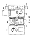
mask 2 and thewafer 3 are disposed within a predetermined closed ambience in an X-ray exposure apparatus, and then the pattern exposure is carried out. It is also proposed therein that themask 2 and thewafer 3 are disposed in a He gas ambience from the standpoint of temperature. Furthermore, a part of the inventors has proposed in Japanese Laid-Open Patent Application Publication 178625/1985 that in an X-ray exposure apparatus using an X-ray tube, a state apparatus, mask and wafer transportation apparatus, an alignment apparatus or the like are disposed in a plurality of closed ambiences. - Referring to Figures 4A and 4B, the apparatus disclosed in the above-mentioned Japanese Laid-Open Patent Application will be described. The wafer is contained in a cassette, which is contained in turn in a wafer loading
cassette accommodating chamber 402. The exposed wafers are contained in a cassette in a wafer unloadingcassette accommodating chamber 403. The mask having a pattern to be transferred is contained in a cassette, which is in turn contained in a maskcassette accommodating chamber 404. - The mask and the wafer are aligned with each other by an
electron beam device 411 shown in Figure 4B in themain chamber 401, and thereafter they are shifted as a unit into anillumination chamber 405, where the pattern exposure is effected with the use of the radiation source, that is, theX-ray rube 410. Between the chambers, shut-off valves are disposed between respective chambers to maintain the ambiences thereof independently from each other, although Figure 4B shows only the shut offvalve 409 between theillumination chamber 405 and themain chamber 401. - A SOR X-ray exposure apparatus is proposed in "Proceeding of SPIE, Vol. 448, 1983, p. 104", for example. Figure 5 shows this apparatus schematically. This apparatus includes a so-called vertical stage which is movable in the vertical direction. The pattern exposure to the
X-rays 1 is performed while themask 2 and thewafer 3 being supported on the stage. - Taking as an example a dynamic random access memory which will hereinafter be called "DRAM" which is recently a kind of standard of the density of the semiconductor chip or device, 64 MB DRAM requires the line width of 0.3 - 0.4 micron, and more than 100 MB DRAM requires 0.25 microns of the line width, and therefore an exposure apparatus capable of pattern transfer of this dimension. However, no exposure apparatus capable of such a fine pattern exposure as not more than 0.25 micron has been made practical. In order to accomplish such an exposure apparatus, it is necessary to establish (1) ambience control for stably maintaining the mask and the wafer, (2) removal of contamination such as dust, (3) X-ray exposure for uniformly exposing the pattern transfer area, (4) an alignment with the precision of the order of 1/100 micron and the resolution of the order of 1/1000 micron and others.
- Accordingly, it is a principal object of the present invention to provide an exposure apparatus which executes key processes in the semiconductor device manufacturing, capable of manufacturing semiconductor devices of 64 MB or higher density.
- It is another object of the present invention to provide a SOR X-ray exposure apparatus which uses X-rays from the SOR source and which can transfer the fine pattern on the mask onto a resist on a semiconductor wafer.
- It is a further object of the present invention to satisfy the requirements of the above-described (1) - (4) to accomplish a practical X-ray exposure apparatus.
- In order to realize the manufacturing of the semiconductor devices having a pattern including lines of approximately 0.25 microns width, a very high precision is required to the exposure apparatus.
- Table 1 shows various factors of the registration accuracy which is the major item of accuracy required for the semiconductor exposure apparatus and allocations thereof.
Table 1 (unit: micron) Items Reg. Precision Mask manufacturing error 0.025 Wafer processing error 0.025 Stage accuracy 0.025 Alignment accuracy 0.025 Optical system 0.025 Other errors in exp. apparatus 0.025 Registration accuracy 0.06 - The "other errors in the exposure apparatus" in the above Table contains deformation or strains of the mask and the wafer due to heat. As will be understood from Table 1, the deformation of the mask and the wafer permitted in the exposure apparatus, the deformation permitted during the exposure, are 0.01 micron at maximum.
- Referring to Figures 6A and 6B, natures of a
typical SOR source 4 will be described. In Figure 6A, theSOR source 4 is schematically shown as an orbit of electrons. TheX-rays 1 are produced by brmsstrahlung of electrons accelerated to an extent of a relativistic velocity. The X-rays thus produced have a power profile which is Gaussian, in the vertical direction V with a divergence angle of several mRad. at maximum and with substantial uniformity in the horizontal direction H over a length open to the orbit of the electrons. The profile is generally trapezoidal. This profile is the one detected by anX-ray detector 1551 shown in Figure 15 for example, at an exposure position where the mask and the wafer are present during exposure. - A wavelength used in the SOR X-ray lithography according to the present invention is within a range of 5 - 15 angstroms. The electron energy accelerated to the relativistic velocity is approximately 0.5 - 1.0 GeV. Figure 6B shows spectral strength characteristics for the respective wavelengths at various points on a path of the exposure beam, more particularly, a position immediately before the mirror, the position immediately after the mirror, a surface of the Be window, a mask surface and a resist surface in the order from the
SOR source 4, when the X-ray exposure apparatus is constituted by disposing the mirror for reflecting the X-rays and the Be window between theSOR source 4 and the mask. It is understood from this Figure, 5 - 15 angstrom wavelength range is preferably in the SOR X-rays lithography. From the same, it is understood that the SOR has continuous spectral characteristics. - Figure 7A shows a mask using inorganic material for the
substrate 201, and Figure 7B shows the same using organic film. In Figure 7A, thesubstrate 201 joined to theframe 203 is constituted by a silicon wafer, and a silicon nitride, for example, is laminated in thin film in apattern area 701 in which an absorber material pattern is to be formed. Or, the silicon wafer is laminated by etching. In this case, the thickness of the substrate in thepattern area 701 is approximately 2 microns. In the example of Figure 7B, an organic film having a thickness of 20 - 10 microns is bonded to theframe 203. An example of the material of the organic film, there is polyimide. - Referring back to Figure 2 showing the proximity exposure system, the distance between the mask and the wafer during the exposure, which will hereinafter be called "proximity gap", is approximately 10 - 50 microns.
- Table 2 shows temperature rise of the silicon nitride mask of Figure 7A and a polyimide mask of Figure 7B when the ambience in the space between the mask and the wafer is vacuum, air or He.
Table 2 (Unit: degree) Ambient Medium Silicon Nitride Mask Polyimide Mask Vacuum §60 §60 Air 1.17 1.18 He 0.343 0.351 - The data of the above Table is on the basis of the X-ray power of 120 mW/cm on the mask surface and on the thermal emissivity of 0.5 in the vacuum. In view of the facts that the sensitivity of the resist material at present is the approximately several tens mJoule - one hundred mJoule/cm² and that the transmissivity of the mask substrate to the X-rays is approximately 50 %, the above data are appropriate. As will be apparent from the Table, in order to prevent the thermal strain, it is preferable that the space between the mask and the wafer is filled with He gas. Therefore, in the present invention, the alignment between the mask and the wafer and subsequent pattern exposure are performed while the mask and the wafer are within He ambience chamber. By containing the mask and the wafer in the chamber, the problems of the contamination such as dust can be solved. Further, in the apparatus of the present invention, the temperature, pressure and purity of the gas functioning as a thermal conduction medium in the chamber are controlled with high precision so as to stabilize the X-ray transmissivity in this ambience, as in the vacuum.
- Referring to Figures 8A, 8B, 9A and 9B, the differences between the whole surface exposure system and the scanning exposure system (scanning mirror exposure system) will be described. Figure 8A illustrates the whole surface exposure system wherein the
X-rays 1 are applied simultaneously to the entirety of thepattern area 701. Figure 8B illustrates strains of the mask resulting from this system. Figure 9A illustrates the scanning exposure system wherein theX-rays 1 in the form of a sheet beam scan thepattern area 701 sequentially. Figure 9B shows the mask strains or deformations resulting from this system. The X-rays produced from the SOR has a very small divergence in the vertical direction, and therefore, the half peak width of the X-ray power profile is only approximately 10 mm even if the exposure position is away from the SOR emitting point by a distance of 10 m. Therefore, in order to reduce the exposure period of the scanning exposure system (the same in the scanning mirror exposure system) to such an extent as being comparable to that of the hole surface exposure system, the strength of the X-ray applied to the mask should be several times that of the whole surface exposure system. This increases the mask strain. - Table 3 shows the temperature rise and the mask deformation in the whole surface exposure system as compared with those in the scanning mirror exposure system.
Table 3 (Unit: degree, micron) Exposure System Silicon Nitride Mask Polyimide Mask Temp. Rise Max. Strain Temp. Rise Max. Strain Scanning Mirror 0.5 Hz 1.34 0.016 1.40 0.094 8 Hz 1.22 0.015 1.22 0.082 1000 Hz 0.343 0.0084 0.351 0.046 Whole Surface Exp. 0.343 0.0084 0.351 0.046 - The data of this Table are based on the material of the wafer chuck 1807 (Figure 18) being alumina (Al) having a thickness of 0.5 mm under the condition that the back surface temperature is constant. With respect to the scanning mirror exposure system, the mirror swing is taken as a parameter.
- As will be understood from the above Table, the mask strain can be made under the tolerable level (0.01 micron) only by the whole surface exposure system and the scanning mirror exposure system, the latter being possible only when the mirror is swung at a high frequency. Also it is understood that a usual polyimide film is not usable as a mask substrate. However, in consideration of the situation wherein the mirror 301 (Figure 3B) is located in a high vacuum ambience of approximately 10⁻⁹ Torr., it is very difficult to realize that the mirror is swung at a high frequency over several tens Hertz. Further, the difficulty is more significant in the scanning exposure system wherein the mask and the wafer are moved together.
- Therefore, the present invention employs the whole surface exposure system.
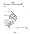
- In the exposure apparatus, the accuracy of the pattern line width is required to be 5 - 10 % of the minimum width of the line to be transferred. In the exposure apparatus capable of exposing 0.25 micron of the minimum line width, the pattern line width accuracy is 0.012 micron. This means that the uniformity of the X-ray illuminance over the entire exposure area (pattern area 701) or the uniformity of the amount of the exposure over the entire exposure area is required to be approximately ±2.5 %. On the other hand, the strength profile of the SOR X-rays, as described hereinbefore, is in the form of the Gaussian function in the vertical plane, and therefore, it is not easy to profile the uniformity of approximately ±2.5 % in the amount of the exposure over the entire exposure area in the whole surface exposure system. If the illuminance is made uniform over the entire exposure area, it cannot be avoided to use only the central portion of the Gaussian distribution, with the result that the efficiency of use of the X-ray energy is low. The present invention, adopts the exposure system shown in Figures 10A and 10B so as to solve those problems. In this system, the X-rays from the emitting
point 1001 in the SOR source are incident on theX-ray mirror 1002 at a low glancing angle, and the X-rays diverged by themirror 1002 are applied on the mask. Themirror 1002 is designed such that the minimum illuminance of the X-ray strength profile in the exposure area is maximum under the set conditions of the exposure apparatus. - Figure 11 shows the X-ray strength profile in the exposure area in this example. As will be understood, the illuminance is significantly different at the central area and the marginal areas of the exposure area. In this system, the illumination distribution can include ±10 % difference in the exposure area. However, in the exposure system, the non-uniformity of the illuminance is corrected by the
shutter mechanism 1003 during the exposure, so that the uniform exposure is effected over the entire exposure area. - The shutter mechanism will be briefly described in conjunction with Figure 10B. A
steel belt 1009 is trained between a drivingdrum 1009 and anidler drum 1001 and is provided with arectangular aperture 1012 having aleading edge 1004 and atrailing edge 1005. Y axis is perpendicular to the optical axis of the SOR X-ray and is substantially vertical. A t-axis represents time. Acurve 1006 indicates movement of theleading edge 1004, and acurve 1007 indicates the movement of the trailingedge 1005. The shutter mechanism drives the drivingdrum 1009 so that the exposure period ΔT(y) at each point on the Y axis is different corresponding to the illuminance profile shown in Figure 11, by which the amount of exposure (= exposure period x illuminance) is uniform over the entirety of the exposure area. - In the exposure apparatus (Figure 5) disclosed in the above-mentioned "Proceeding of SPIE, Vol. 448, 1983, p. 104", the path of the X-ray from SOR source is once stopped by Be window, and thereafter the wafer is exposed to the X-ray through the wafer in the air.
- Figure 12 shows the dependency of the thermal conductivity to pressure for the air and He. It will be understood from this Figure that the air has a lower thermal conductivity than He under the same pressure. Therefore, in consideration of the strain of the mask described with Tables 2 and 3, it is difficult to achieve the object of the present invention by the exposure in the air. In consideration of this, the present invention adopts the exposure in the closed He ambience for which the temperature, pressure and purity are controlled with high precision. In addition, in order to meet the SOR X-ray source, the conveying mechanism and the exposure stage are of vertical type, and the mask and the wafer are conveyed within a completely closed ambience. By this, in the SOR X-ray exposure apparatus, a high throughput and reduction of influence by particles (dust) and contamination are achieved.
- Furthermore, in the present invention, a wafer stage is controlled in 6 axes (X, Y, Z, ϑ (= ωz, ωx, ωy)), and the mask stage is controlled in ϑ axis only, so as to achieve the high accuracy of the mask stage, in view of (1) that the optical axis of the X-ray from the SOR source hardly changes, (2) that the accuracy of the mask is sufficient as described hereinbefore and (3) that in the SOR X-ray exposure, the stability in the relation between the optical axis of the X-ray from the SOR source and the mask is most important.
- In the present invention, the mask stage is rotatable about ϑ direction in order to align the orientation of the mask with the movement direction in X and Y axes of the wafer which is step-and-repeat-exposed. In order to accomplish this mask alignment with great precision, a reference mark is provided on the wafer stage, and the mask alignment is effected using the reference mark.
- These and other objects, features and advantages of the present invention will become more apparent upon a consideration of the following description of the preferred embodiments of the present invention taken in conjunction with the accompanying drawings.
-
- Figure 1 is a perspective view showing general arrangement of an exposure apparatus according to an embodiment of the present invention.
- Figure 2 illustrates X-ray proximity exposure.
- Figures 3A, 3B and 3C are perspective views illustrating various types of exposure systems.
- Figure 4A is a top plan view of a conventional X-ray exposure apparatus.
- Figure 4B is a sectional view of a conventional X-ray exposure apparatus.
- Figure 5 is a side view of a conventional SOR X-ray exposure apparatus.
- Figure 6A is a perspective view of SOR ring illustrating a property of the X-ray strength distribution.
- Figure 6B is a graph of X-ray power vs. wavelength.
- Figure 7A is a perspective view of a mask using inorganic substrate material.
- Figure 7B is a perspective view of a mask using organic substrate material.
- Figure 8A is a sectional view of a mask for illustration of thermal strain.
- Figure 8B is a sectional view of a mask for illustration of thermal strain of a mask.
- Figure 9A is a top plan view of a mask showing thermal strain distribution corresponding to Figure 8A.
- Figure 9B is a top plan view of a mask illustrating thermal strain distribution of a mask.
- Figure 10A illustrates the exposure apparatus according to the present invention, schematically.
- Figure 10B is an illustration of shutter.
- Figure 11 is a graph showing an X-ray strength profile in an exposure area in an exposure apparatus according to the present invention.
- Figure 12 is a graph of thermal conductivities of gases vs. pressure.
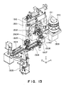
- Figure 13 is a perspective view of an exposure unit according to an embodiment of the present invention.
- Figure 14 is a perspective view of an X-ray mirror unit.
- Figure 15 is a perspective view of an exposure unit and a shutter unit.
- Figure 16 is a side view illustrating arrangement of the exposure and shutter units.
- Figure 17 is a perspective view illustrating a stage.
- Figure 18 is a perspective view of a fine wafer stage.
- Figure 19 is a perspective view of a mask ϑ stage.
- Figure 20 is a top plan view illustrating arrangement of a distance measuring laser optical system.
- Figure 21 shows an optical arrangement of a prealignment system.
- Figure 22 is a perspective view of the prealignment system.
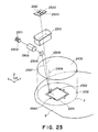
- Figure 23 is a perspective view illustrating optical elements in a pickup station.
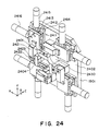
- Figure 24 is a perspective view of a fine automatic alignment unit.
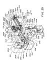
- Figure 25 is a perspective view of a wafer conveying system.
- Figure 26 is a perspective view of a mask conveying system.
- Figure 27 is a top plan view of a mask conveying station.
- Figure 28 is a perspective view illustrating a mask cassette loader.
- Figure 29 is a side view of the mask cassette loader illustrating its operation.
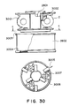
- Figure 30 is a side view of a mask cassette.
- Figure 31 is a perspective view of the apparatus illustrating chambers.
- Figure 32 is a block diagram of gas supply and discharge system.
- Figure 33 is a schematic view illustrating a wafer load locking mechanism.
- Figure 34 is a schematic view illustrating a mask load locking mechanism.
- Figure 35 is a schematic view illustrating a gas supply and discharging system for pressure and purity control and for mirror port.
- Figure 36 is a block diagram for the entire control system for the X-ray exposure apparatus.
- Figure 37 is a block diagram for a console unit.
- Figure 38 is a block diagram of a main unit.
- Figure 39 is a block diagram of a control unit for the main assembly.
- Figure 40 is a block diagram for fine automatic alignment and fine automatic focusing.
- Figure 41 is a block diagram of an automatic prealignment control system and a automatic prefocusing system.
- Figure 42 is a block diagram of a pickup stage control system.
- Figure 43 is a block diagram of a shutter control system.
- Figure 44 is a block diagram of a pulse generator circuit.
- Figure 45 is a block diagram of a stage control system.
- Figure 46 is a block diagram of a conveyance control system.
- Figure 47 is a block diagram of a mirror control system.
- Figure 48 is a block diagram for an ambience control system.
- Figure 49 is a flow chart illustrating an overall operation.
- Figure 50 is a flow chart for start-up operation after long rest.
- Figure 51 is a flow chart of operation of gas supply and discharge operation for the main chamber at a start-up operation after long rest.
- Figure 52 is a similar flow chart for a wafer loading chamber.
- Figure 53 is a flow chart for initializing various actuators at a start up operation after long rest.
- Figure 54 is a flow chart for the operations for shutting off the apparatus for a long period.
- Figure 55 is a flow chart illustrating gas supplying and discharging operations for shutting off the apparatus for a long term rest.
- Figure 56 is a similar flow chart for the wafer loading chamber.
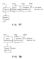
- Figure 57 is the similar flow chart for the mask chamber.
- Figure 58 is a flow chart for taking out a wafer supplying carrier.
- Figure 59 is a flow chart illustrating a wafer supplying carrier setting.
- Figure 60 is a flow chart for mask cassette taking out operation.
- Figure 61 is a flow chart for mask cassette setting operation.
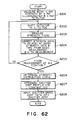
- Figure 62 is a flow chart illustrating X-ray strength profile measurement.
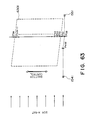
- Figure 63 illustrates measurement position for the X-ray strength profile measurement position.
- Figure 64 is a graph of X-ray strength vs. measurement positions.
- Figure 65 is a graph of exposure area vs. exposure period of time in an example.
- Figure 66 is a graph illustrating shutter speed and control data setting.
- Figure 67 is a schematic view illustrating the shutter system.
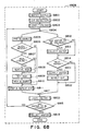
- Figure 68 is a flow chart for exposure process.
- Figure 69 is a flow chart of wafer supply operation.
- Figure 70 is a flow chart for orientation flat detection.
- Figure 71 is a graph illustrating orientation flat detection.
- Figure 72 is a top plan view of a wafer in coordinates of the stage.
- Figures 73A and 73B are flow charts illustrating loading and unloading operations.
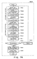
- Figure 74 is a flow chart illustrating a prealignment operation.
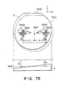
- Figure 75 is a top plan view illustrating positions of prealignment mark.
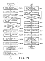
- Figure 76 is a flow chart for a mask taking up operation.
- Figure 77 is a flow chart illustrating a mask setting operation.
- Figure 78 is a flow chart illustrating mask alignment operation.
- Figure 79 is a side view illustrating a mask alignment mark position.
- Figure 80 is a flow chart illustrating a step-and-repeat exposure.
- Figure 81 is a schematic view illustrating an automatic wafer focusing operation.
- Figure 82 is a side view illustrating an automatic wafer alignment.
- Figure 83 is a flow chart illustrating a wafer taking up operation.
- Figure 84A and 84B are front and side sectional views of the exposure unit.
- Figure 85 is a block diagram for a control of a vibration suppressing system.
- Referring back to Figure 1 which shows the general arrangement of the exposure apparatus according to an embodiment of the present invention, an electron accelerator or an electron accumulating ring which will hereinafter be called "SOR ring" 4 produces SOR rays, and the electron orbit is horizontal. In the illustrated example, only one SOR ray emitting port is shown, but two or more of them may be provided. A
mirror unit 101 is disposed between theSOR ring 4 and anexposure unit 102, and it contains anX-ray mirror 1401, which will be described in detail in conjunction with Figure 14, to change divergence of the SOR rays to desired extent. TheX-ray mirror 1401 is in a vacuum of approximately 1x10⁻⁸ - 1x10⁻¹⁰ Torr. Abeam duct 120 connects theSOR ring 4 and themirror unit 101 while keeping the vacuum of approximately 1x10⁸ - 1x10⁻¹⁰ Torr. - The
exposure unit 102 is contained in amain chamber 3101 which will be described in conjunction with Figure 31. Themain chamber 3101 is filled with a highly pure He gas having a purity of not less than approximately 99.99 %. As shown in Figure 13, in this ambience, there are contained astage apparatus 1301 for carrying and/or holding amask 2 and awafer 3, a measuringoptical system 1312 for determining the stage position, aprealignment system 1307 for measuring a relative positional deviation between thewafer 3 and themask 2 for preliminary alignment thereof, afine alignment system 1302, anexposure shutter apparatus 1308 for providing thewafer 3 with proper X-ray exposure amount, a wafer supplying and taking upapparatus 1303 for supplying and taking up wafers, aninjector 1304 for conveying thewafer 3, awafer traverser 1306, an orientation flat detectingstage 1305 for aligning crystalline orientation of thewafer 3, a maskaccommodating apparatus 1301 for accommodatingmasks 2, amask cassette loader 1309 for loading and unloading themask 3 relative to themask cassette 1310, amask conveying apparatus 1311 for transferring themask 3 between themask cassette 1310 and amask ϑ stage 1999 which will be described in conjunction with Figure 19, and other auxiliary apparatuses. The main chamber is fixed on avibration suppressing base 8405, as will be shown in Figure 84. Thevibration suppressing base 8401 has threeair suspensions vibration suppressing base 8401. Thevibration suppressing base 8401 is a rigid assembly for supporting thevibration suppressing base 8405 and the main chamber. Thevibration suppressing base 8401 has a fluid bearing (not shown) mounted thereto, the fluid bearing being effective to supply air to lift the base by the pressure from the floor. The fluid bearing provides a reduced frictional resistance relative to the floor during the adjustment of the entire exposure unit setting, and therefore, it makes fine positional setting possible. - Between the
mirror unit 101 and theexposure unit 102, thebeam duct 121 is disposed, in which shut-offvalves Be window 3512 as shown in Figure 35, and to which each of theunits beam duct 121 is supported on the floor through a supportingframe 123. The inside of thebeam duct 121 is kept under vacuum condition of approximately 1x10⁻⁶ - 1x10⁻¹⁰ Torr by a vacuum pump disposed between themirror unit 101 and Bewindow 3512. - An
electric control unit 103 functions to control themirror unit 101, theexposure unit 102, a constanttemperature maintaining unit 104, a dischargingunit 105, asupply control unit 106 and as an input board for operation, and also serves for supplying and receiving coordination signals with theSOR ring 4 and for supplying and receiving safety signals in connection with inlet door of the operation room. The constanttemperature maintaining unit 104 is effective to supply heated fluid to heat generating parts such as themirror unit 101, theexposure unit 102 or the like to absorb the heat from those parts to keep the temperature thereof constant. The dischargingunit 105 discharges fluid in the exposure unit, and controls themirror unit 101 and thedischarge pump 122. Thesupply control unit 106 controls high pressure air, N₂ and He gases used in themirror unit 101 or in theexposure unit 102. - As briefly described in the foregoing, the exposure apparatus according to this embodiment, includes various constituent units. The advantageous effect provided by the unit structure will be described. In an exposure method using the X-rays provided by the
SOR ring 4, a role of theX-ray mirror 1401 for controlling divergence of the X-rays is important as will be decribed hereinafter in more detail. It will be difficult to achieve the exposure by SOR X-ray without theX-ray mirror 1401. - The role thereof includes selection of the wavelength appropriate for the exposure, reduction of the distance between the
SOR ring 4 and theexposure unit 102 by creating an appropriate X-ray strength distribution and an appropriate X-rays. By the selection of the wavelength, the contrast of themask 2 can be assured, and by creating an appropriate X-ray strength distribution, the exposure system is not changed in dimensions by heat. By controlling the divergence angle, the distance between theSOR ring 4 and theexposure unit 102 can be made practical. In summary, by use of theX-ray mirror 1401, a practical SOR exposure system can be provided. - The influence to the exposure system by the
SOR ring 4 in the exposure system using the SOR rays, will be considered. Generally, the outside dimension of theSOR ring 4 is approximately 2 - several tens meter, and the weight thereof is several tens - 300 ton. Therefore, the exposure system is required to be relatively freely movable toward the emitting direction of the SOR rays. Around theSOR ring 4, a radiation blocking wall having a thickness of approximately several tens cm is disposed. - It is considered in the exposure system that the wall should be conveniently near the
SOR ring 4 since then it is as if remote fron floating radiation. In the SOR rings presently available, the positions of the wall is widely different, in one of which the wall is very close to the SOR ring and in another of which it is fairly away by as large as several meter. Therefore, it is preferable in the exposure system that it is usable irrespective of whether the wall is between theSOR ring 4 and themirror unit 101 or between themirror unit 101 and theexposure unit 102. In view of those, it has been found that the image exposure system can be made practicable by constituting various parts of the apparatus as the mirror unit, the exposure unit, the electric control unit or the like. In the foregoing, the general arrangement of the exposure system using the SOR rays is generally described. - The description will now be made as to each of the unit in somewhat detail.
- The
mirror unit 101 has to be directly connected to theSOR ring 4, and therefore, it has a vacuum system independent from that of theexposure unit 102. The unit in its entirety is required to be aligned relative to the SOR rays in six axis directions (X, Y, Z, ϑ, ωx, and ωy). In order to allow theentire mirror unit 101 to be movable in the X and Z directions, a fluid bearing is used at the bottom of the unit. The movement in the Y direction and the rotational motions about X, Y and Z axes are effected by a mirror position or pose adjusting apparatus 1406 (Figure 14) directly contacted to theX-ray mirror 1401. TheX-ray mirror 1401 which receives the SOR rays directly is prevented from thermal deformation by supplying a liquid medium having a constant temperature adjacent thereto. Between theX-ray mirror 1401 and theSOR ring 4, an aperture 1409 (Figure 14) is provided so as to avoid the possible damage by unnecessary X-ray application. - The
exposure unit 102 is required to be aligned in the six axes similarly to the case of themirror unit 101, relative to the SOR optical axes of theSOR ring 4 and themirror unit 101. To achieve this, a fluid bearing is provided at the bottom of the unit so as to make easier movement of theexposure unit 102 in X and Z directions and the rotation (ωy) about the Y axis. The rotational motion (ωx, ϑ) about X and Z axes and the motion in the Y direction are effected by controlling pressure of theair suspension - Since the
exposure unit 102 receives the SOR rays, the problems arising from the SOR rays are to be solved. If the inside of the main chamber 3101 (Figure 31) among the constituent elements of theexposure unit 102 can be made vacuum, the problems will be reduced, but it is not preferable to adopt the vacuummain chamber 3101 so as to deal with the heat of mask, which will be described hereinafter. Therefore, in this embodiment, the main chamber is filled with He (H is possible) which absorbs low percentage of the SOR rays, particularly, X-rays. This necessitates an introduction of an X-ray inlet window to separate the vacuum ambience and the He ambience. As for the material for the window, Be is appropriate. The X-ray absorption by the He and the Be reduces the exposure energy, and therefore, the absorption should be minimized. Therefore, it is preferable that the pressure of the He gas is minimized and that the thickness of the Be window is minimized. The pressure of He is determined in consideration of the thermal conduction property and distance through which the X-rays pass. - For the reasons which will be described hereinafter, the pressure of He is 100 - 200 Torr, and the purity is 99.99 %. The thickness of the Be window is determined in consideration of the He pressure and the structure therearound. The thickness thereof can be approximately 20 microns when the gas control system and discharging system which will be described hereinafter, are used. The distance through which the X-rays pass is preferably not less than 30 cm. In order to maintain the purity of He, it is preferable to discharge the
main chamber 3101 to the extent of the vacuum of approximately 1 - 10⁻⁴ Torr, and then He is introduced. The amount of contamination gases introduced into themain chamber 3101 is minimized, and it is preferable to provide a supply control unit so as to maintain the purity of He gas against the leakage of the contamination gases. - The description will be made as to means for providing the precisions. The exposure system is generally required to be capable of exposing 30 mm x 30 mm area of the wafer. A thermal expansion coefficient of an ordinary silicon wafer is approximately 4x10⁻⁶/°C. Therefore, the dimensional change per 1 °C in 30 mm length is 0.12 micron. Since in the exposure system it is desired that the change is not more than 0.001 - 0.01 micron, the temperature change at the position where the
wafer 3 is present is to be maintained within 0.01 - 0.1 °C. This requirement is achieved in the present invention by flowing a constant temperature fluid to the portion where the wafer is present or the portion where the dimensional change should be controlled. In the exposure system, the mask pattern is transferred to a predetermined position of the wafer, and the reproduction accuracy of the positioning relative to each other is desired to be 0.02 - 0.05 micron. In order to accomplish this, the mask and wafer are mechanically strongly fixed and guided together, but the mechanical rigidity therebetween is limited. The positional deviation therebetween results from temperature change of the associated members and deformation by external vibrations thereof. - The temperature change is suppressed by the above-mentioned constant temperature maintaining means, and the influence of the external vibration is prevented via a structure by which the transmission of the vibration is shut by the air suspensions 8402 - 8404 mounted between the
vibration suppressing base 8405 and thevibration suppressing frame 8401 shown in Figure 84. Between theX-ray duct 121 and theexposure unit 102, there is a soft material portion such as bellows to prevent transmission of the vibration from theduct 121 to beexposure 102. The means for obtaining the precisions have been described above. - In the foregoing, the general arrangement of the exposure system using the SOR rays particularly the X-rays have been briefly described.
- Detailed description of the exposure system according to this embodiment of the present invention will now be described.
- Referring to Figure 13, there is shown an internal structure of the exposure unit, wherein the portions downstream of the Be window 3512 (Figure 35) with respect to travelling direction of the SOR rays.
- The
exposure unit 102 is to align the pattern on themask 2 to be transferred is aligned with a predetermined position of the resist on thewafer 3, and transfer it on thewafer 3 using the X-rays. The pattern is in 30 mm x 30 mm area, whereas the wafer has a diameter of several tens mm - several hundreds mm, and therefore, the exposure of the wafer is effected in a step-and-repeat manner wherein one wafer is covered by plural exposures. The precision of the alignment between themask 2 and thewafer 3 is 0.01 - 0.05 micron, and of course, the smaller the better. Since the transfer pattern of one mask is transferred plural times at different areas of the wafer, and therefore, the pattern of the mask is not permitted to have contamination or other defects. From this standpoint, the time period used for other than the exposure, such as the alignment between themask 2 and thewafer 3 should be minimized. Therefore, what should be considered in the exposure unit is that it is provided with means for precisely conveying themask 2 and thewafer 3, which does not produce contamination and which does not spend wasteful time. - The internal structure of the
exposure unit 102 is determined in consideration of the above. Astage 1301 is provided to holdwafer 3 and themask 2 and align them, and therefore, it is an important element of theexposure unit 101. Since thestage 1301 is vertical so as to hold thewafer 3 perpendicular to the optical axis of the SOR rays and thewafer 3 is moved in three dimensions (X, Y, Z) with positioning resolution of not more than 0.01 micron. The stage is guided by a fluid bearing and an elastic linkage so as to minimize the heat generation, vibration generation and contamination. The constant temperature fluid is supplied to the neighborhoods of a driving means, fluid bearing guides or the like where the temperature change can occur, so as to prevent the temperature change of the structural element associated. Thestage 1301 is provided with other constituent sub-units and the rigidity between the mask and the wafer is such that the minimum characteristic frequency is 200 - 300 Hz. - A
fine alignment system 1302 serves to detect the positional relation between thewafer 3 and themask 2. The fine alignment system 1032 comprises an optical system (which will be described hereinafter in detail) for detecting the positional relation between thewafer 3 and themask 2 in three dimensions (X, Y, Z) and means for moving the optical system. Thefine alignment system 1302 is disposed around the periphery of the exposure X rays so as not to block the exposure X-rays. Also, it is mounted to thestage 1301. Thefine alignment system 1302 is on thestage 1301, and is close themask 2, and therefore, the constant temperature fluid is supplied to the neighborhood of the heat generating parts such as the illumination source for the fine alignment, the electric circuit and actuators therefor to prevent the temperature change. - A
prealignment system 1307 is to determine the position of thewafer 3 introduced thereinto, relative to thestage 1301. The prealignment system determines the position of thewafer 3 relative to thestage 1301 in the six axes (X, Y, Z, ϑ, ωx, ωy), by which the operating period of thefine alignment system 1302 can be shortened. On the basis of the results of the measurement by theprealignment system 1307, thestage 1301 is controlled so as to avoid thewafer 3 to abut themask 2. - The
system 1307 is on the top surface of thestage 1301, and therefore, the constant temperature current is supplied to the heating generating parts so as to avoid the temperature change during the operation of this system. The light source is a significant heat generating part, and it is relatively quickly consumed, and therefore, it is disposed outside themain chamber 3101 for the purpose of easy exchange of the light source for the prealignment and of minimizing the influence of the heat generation. Using optical fibers, only a required specter is introduced into the system. - An exposure shut
apparatus 1308 is to control the exposure energy by allowing and stopping passage of the X-rays. In this exposure system, the X-rays emitted from theSOR ring 4 are reformed into an appropriate shape by the mirror 1401 (Figure 14), as described hereinbefore, the efficiency of use of the SOR rays is higher if the non-uniformity of the strength of the energy in the Y axis direction resulting from the nature of the SOR ray radiation. In order to eliminate the non-uniformity in the Y direction, theexposure shutter apparatus 1308 is to effectively operate. - To meet those requirements, the shutter is in the form of a focal plane shutter. When the
shutter apparatus 1308 operates, thewafer 3 and themask 2 have been positionally aligned in the precision of order of 0.01 micron, and therefore, the production of vibration should be minimized. In consideration of this, the shutter films (steel belts main chamber 1301, by which the influence to the precision in the alignment between themask 2 and thewafer 3 is minimized. - In this
apparatus 1308, the constant temperature fluid is supplied to the portion where the heat is produced to suppress the temperature change. - An orientation flat detecting
stage 1305 serves mainly to determine the orientation of crystalline of thewafer 3 being conveyed and the center of thewafer 3 and to determine thewafer 3 rotation and to position thewafer 3 center in place relative to thestage apparatus 1301. The detectingstage 1305 comprises a plurality of linearly movable stages in X and Y directions, a rotating stage on one of the aforementioned stages and an optical system for measuring the dimension of the wafer at its ends. The rotating stage is provided with means for attracting and holding thewafer 3. In the detectingstage 1305, the relative positional relation with the above-describedstage 1301 is important, and therefore, it is directly mounted to thestage 1301. To the heat generating parts such as a driving actuator, the constant temperature fluid is supplied to prevent the temperature change. - A
wafer traverser 1306 functions mainly to convey thewafer 3 from the orientation flat detectingstage 1305 to thestage 1301 and in the opposite direction. Thewafer traverser 1306 moves in the Z direction on the orientation flat detectingstage 1305 and at the wafer transferring position of thestage 1301 and also moves in the X direction from the orientation flat detectingstage 1305. A plurality of wafer hands are provided to supply and take up the wafers, exclusively. They are moved in the opposite directions along the X axis. Each hand of thewafer traverser 1306 is required to stop at a predetermined position on thestage 1301, and therefore, it is directly mounted to a member of thestage 1301. The heat generating parts such as a driving actuator or the like is supplied with the constant temperature fluid so as to prevent the temperature change thereof. - An
injector 1304 has a main functions to dispense thewafer 3 from and accommodate it into a wafer carrier of a wafer supply and take upapparatus 1303 and to supply thewafer 3 to or remove it from the orientation flat detectingstage 1305. Theinjector 1304 is capable of moving a wafer supporting surface of a wafer hand between horizontal position and vertical position, and the hand is movable in the X (or Z) direction, and is movable about the Y axis. Theinjector 1304 is mounted to the wall of thechamber 3101. The heat generating elements of theinjection 1304 is supplied with a constant temperature water to prevent the temperature change. - A wafer supplying and taking up
elevator 1303 serves mainly to step a wafer carrier containing or not containing thewafers 3 in the X-axis direction to supply or collect the wafers. Thewafer elevator 1303 is mounted to a chamber isolated by a gate valve, which will be described hereinafter. A driving station thereof is disposed in the air from the stand point of contamination prevention. - A
mask cassette 1310 is an accommodating chamber for accommodating 20 masks. Themask cassette 1301 is hermetically sealed so as to prevent the mask from contacting the air. Amask cassette loader 1309 has main functions to hold themask cassette 1310, to open or close themask cassette 1310 and to set a selected mask to a position for themask conveying apparatus 1311 to receive it. Themask cassette loader 1309 is directly mounted to a container isolated by a gate valve, which will be described hereinafter. The main function of themask conveying apparatus 1311 is to convey themask 2 between themask cassette 1310 and a mask chuck 1903 (Figure 19). Since themask 2 is fragile, the consideration is paid so as not to produce a shock, not to produce contamination by swinging movement or the like, and particularly not to impart a mechanical deformation to themask 2 when it is set on themask chuck 1903. The most important point to meet those requirements, is a very accurate track of the hand for the holding themask 2. The hand is rotatable about a Z-axis on a table movable in the X direction. At the rotational stopping positions in the clockwise and counterclockwise direction, it is abutted to stop pins at a constant pressure. As regards the X-axis direction, the correct track of motion is provided by an optical position detection and employing a driving system capable of correct movement track. A measurementoptical system 1312 has a major function of measuring a position of a wafer fine movement stage 1899 (Figure 19). The measurementoptical system 1312 includes an interference device using a laser beam source in the form of a Mickelson interferometer having a reference point on a main frame 1701 (Figure 17). The laser source and the photoreceptor of the measurementoptical system 1312 are disposed outside the main chamber. The in-between optical window is hermetically mounted to themain chamber 3101. The laser source and the photoreceptor are mounted directly to themain frame 1701, by which the optical axis is prevented from mechanical deformation. In the foregoing, the subordinate units of theexposure unit 102 are explained. - The subunits will be further explained. The pattern of the
mask 2 is transferred onto thewafer 3 at a position behind themask ϑ stage 1999 of thestage 1301 in the Z direction. In this system, the highest precision is desired at the transfer position. What is important is the relative positional relation between the mask and thewafer 3 which should be with minimum positional error. There are various factors for the alignment error, but among them, the stability of the measurementoptical system 1312 should be established. The transfer position is so disposed as not to be adjacent the center of the Y axis guiding shaft of thestage 1301, since then the rigidity of the stage is enhanced. In consideration of this, the transfer position is located above the movable range of thestage 1301 in the Y direction. By doing so, the distance from the interferometer of the measurementoptical system 1312 and the stage position measuring mirror can be reduced, and therefore, the influence of the ambience in the chamber to the measurement accuracy can be reduced. The movement distance of the stage in the Y direction is longer than that in the X direction, in consideration of the fact that counter balance or moment balance can be easily used in the Y direction. - Therefore, the shape of the
stage apparatus 1301 is such that it is longer in the Y direction, and the measurementoptical system 1312 is disposed on the top surface of the frame 1701 (Figure 17) in the Y direction. The transfer position is disposed topmost possible position in the Figure. With those arrangement, the number of movable parts above themask 2 and thewafer 3 is reduced, so that the problem of contamination falling is eliminated. Also, themask conveying apparatus 1311, the orientation flat detectingstage 1305, theinjector 1304, thewafer traverser 1305 or the like are necessarily disposed at a lower side in the Figure of the transfer position, and therefore, the transfer position is protected from the dust produced by those subunits. - In this Figure, there are shown an
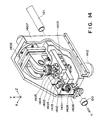
automatic alignment frame 2604 which connects themain frame 1701, themask ϑ stage 1999 and thefine alignment system 1302. - Referring to Figure 14, there is shown an example of a part of the illumination optical system for enlarging the SOR rays in the vertical direction and for projecting the expanded rays to the entirety of the exposure area simultaneously. The X-ray mirror has a convex cylindrical reflecting surface for diverging the SOR rays. The reflecting surface is made of SiC or SiO₂ or Au Pr or the like film on the SiO₂. The reflecting surface is processed with very high precision to provide sufficiently large reflection index for the wavelength region of the X-rays usable for the exposure. The mirror unit includes a
mirror base 1402 for supporting theX-ray mirror 1401, aliquid medium passage 1404 formed in themirror base 1402. In thepassage 1404, a temperature controlled liquid medium is circulated. The SOR rays are partly absorbed by the reflecting surface of theX-ray mirror 1401, and the absorbed energy becomes heat. - A thermal connecting member made of indium thin film or the like is disposed between the back surface of the
X-ray mirror 1401 and the mirror supporting surface of themirror base 1402 and is cross-contacted to the respective surfaces. By this, the thermal resistance from theX-ray mirror 1401 to themirror base 1402 is reduced to promote thermal conduction of the heat produced by the absorption of the SOR ray to the liquid medium circulating in thepassage 1404, thus suppressing the temperature rise of theX-ray mirror 1401. - The mirror unit includes a mirror supporting member which urges the
X-ray mirror 1401 to themirror base 1402. A supporting member supports themirror base 1402. The supportingmember 1414 includes a pipe connected to theliquid medium passage 1404 in themirror base 1402. A bellows 1405 made of metal is connected to avacuum chamber 1408 at its one side and is connected to the supportingmember 1414 at the opposite side. Apose adjusting apparatus 1406 serves to adjust the pose of theX-ray mirror 1401 in plural latitudes and is securedly fixed to the supportingmember 1414. Thebellows 1405 accommodate the relative displacement between thevacuum chamber 1408 and the supportingmember 1414 when the mirror pose adjustingapparatus 1406 moves and adjusts theX-ray mirror 1401. Aframe 1407 rigidly supports the mirror pose adjustingapparatus 1406. Thevacuum chamber 1408 and theframe 1407 are independently fixed to an unshown base, and therefore, the deformation of thevacuum chamber 1408 attributable to the changes in the temperature for the ambient pressure does not influence the pose or position of theX-ray mirror 1401. Therefore, the rigidity of thevacuum chamber 1408 can be decreased to permit reduction of the weight. A discharge port 1411 is connected with adischarge pump 1412 for maintaining a high vacuum in thevacuum chamber 1408. Ashutter 1409 is provided to avoid that theX-ray mirror 1401 receives the SOR rays when it is not necessary, by which the time period during which theX-ray mirror 1401 is dozed with the SOR rays. The reduction of the time period is contributable to reduce the damage of theX-ray mirror 1401 by the radiation. - The
X-ray mirror 1401 is supported with its reflecting surface facing down, and the axis of the cylindrical reflecting surface is horizontal as shown in Figure 10A, and the central axis of the SOR rays is at an angle of 10 mrad - 30 mrad relative to the reflecting surface. - The description will be made with respect to the exposure shut
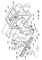
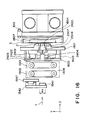
apparatus 1304. As described briefly hereinbefore, the shutter includes not only the function of controlling the exposure period in accordance with the source strength change and the difference of the sensitivity resulting from the material of the resist but also the function of the local exposure period in accordance with the spectral properties and the strength distribution, in the Y direction, of theSOR X-rays 1 reflected by theX-ray mirror 1401. In addition, it is contributable to provide a uniform energy absorption over the entire exposure area of the resist. - Figure 15 shows various elements of the
exposure shutter apparatus 1308 in a perspective view. Figure 16 is a sectional view to show themask 3, thefine alignment system 1302 disposed between the wafer and theexposure shutter apparatus 1308, which are omitted in Figure 15, thus illustrating the arrangements thereof in the direction of the axis of the X-rays. - In this embodiment, the
exposure shutter 1308 comprises two similar units, i.e., amain shutter unit 1501 and anauxiliary shutter unit 1502. As shown in Figure 15, theX-rays 1 which is the exposure beam, as shown in Figure 15, is blocked by thesteel belt 1517 made of stainless steel during non-exposure period. However, during the exposure period, the X-rays pass through a rectangular opening formed in thesteel belt 1517 which functions as aforward exposure aperture 1530 and through thebackward exposure aperture 1533 moved to the position substantially corresponding to theforward aperture 1530 and reach the backwardmain shutter unit 1501. Thesteel belt 1513 of themain shutter unit 1501 is provided, similarly to thesteel belt 1517 of theauxiliary shutter limit 1502, with two openings, i.e. a forward exposure aperture 1503 and thebackward exposure aperture 1533. The function of controlling the local exposure period in the Y direction is accomplished by making different at different Y direction position the time period from the reaching of theleading edge 1531 of theaperture 1530 of themain shutter unit 1501 to the passing of the trailingedge 1532 thereof so that the amount of energy absorption by the resist at each point in the Y direction is constant and optimum. - The
steel belt 1517 is stretched between the drivingdrum 1515 driven by theactuator unit 1518 and theidler drum 1516, and the inside of thesteel belt 1515 is driven by the drivingdrum 1515 through friction. The drivingdrum 1515 is crowned by which the central portion of the drum has a larger diameter than that of the marginal portions by 50 - 100 microns so as to stabilize the movement of thesteel belt 1517 without rolling. Adjacent opposite ends of thesteel belt 1517, a small rectangular openings are formed, one of which is atiming aperture 1534, and the other of which is aposition detecting aperture 1535. They are cooperated with atiming sensor 1536 and with aphotointerruptor 1537, respectively, to produce a starting signal to permit anactuator unit 1518 to be actuated in a predetermined driving pattern and to detect whether the SOR X-rays are blocked or transmitted. Theactuator unit 1518 comprises a motor and an aluminum alloy casing which hermetically contains the motor. The aluminum alloy casing is provided with a water passage, by which the heat produced by the motor is carried over to outside the chamber through an unshown piping. The casing is also effective to prevent the oil used in the motor or the particles produced by the bearing and various contacts from scattering into the exposure ambience. - The mechanical structure of the
main shutter unit 1501 is the same as that of theauxiliary shutter unit 1502, and therefore, the detailed description is omitted for simplicity. - An X-ray detector is mounted to the fine movement stage 1804 (Figure 18) when the two
shutter units X-ray detector 1511, the strength profile of the X-ray can be measured. On the basis of the data obtained, a driving table for driving theactuator unit 1514 is produced, and the correcting drive to provide the constant energy absorption of the resist in the exposure area can be effected. - An X-ray illuminometer is fixed on the
carriage 1542 movable in the X direction perpendicular to the axis of the X-rays and normally, is maintained at a stand-by position away from the exposure area or exposure view angle. It is moved to a predetermined position in the exposure area only during the measuring operation to measure the strength of the X-rays. Thecarriage 1542 is moved and positioned by a driving system constituted by asteel belt 1544, a drivingpulley 1546, anidler pulley 1545 and anactuator unit 1547. - Figure 16 shows the arrangements of the
auxiliary shutter unit 1502, themain shutter unit 1501, theX-ray detector 1551 and theX-ray illuminometer 1541 in the X-ray axis direction. Themain shutter unit 1501 is disposed close to thefine alignment system 1302 which will be described in detail hereinafter. - Figure 17 shows a general arrangement of the mask-wafer alignment stage, more particularly, the
stage apparatus 1301 and the measurementoptical system 1312. Amain frame 1701 which is the base of the entire stage, and the Ycoarse movement stage 1705 is guided using static pressure in a pair of Y coarsemovement guide bars 1706 mounted to themain frame 1701, thus allowing vertical movement. The Ycoarse stage 1705 is connected with abalancing cylinder 1709 mounted to themain chamber 3101, through a pair of balancingbelt 1708 to balance the weight of the Y coarse stage. The Ycoarse stage 1705 is driven and positioned by aY driving cylinder 1707 which is electrically driven, thecylinder 1707 is mounted to themain frame 1701. - Further, X
coarse stage 1710 is guided through static pressure on a pair of X coarsemovement guide bars 1711 mounted on the Ycoarse stage 1705 to permit horizontal movement. The Xcoarse stage 1710 is driven and positioned byX driving cylinder 1712 which is electrically driven, the Xcoarse stage 1710 being mounted on the Ycoarse stage 1705. On the Xcoarse stage 1710, a waferfine movement stage 1899 for finely positioning thewafer 3 and a laserdistance measuring mirror 1810 are mounted. - On an
automatic alignment frame 2604 mounted to themain frame 1701, amask ϑ stage 1999 is mounted. Themain frame 1701 is connected to themain chamber 3101 through aframe connector 1704, and the entire stage is accommodated in themain chamber 3101. - The laser interferometer for distance measuring will be described. It is supported on the upper portion of the
main frame 1701. A laser beam emitted from the laser heads 1720a and 1720b disposed outside themain chamber 3101 is divided into X and Y directions by adistributor unit 1721. One of them is directed to an Xaxis interferometer unit 1722 mounted to theautomatic alignment frame 2604 and is reflected by adistance measuring mirror 1810 and is received by a receiver 1725a to measure the position of the waferfine movement stage 1899 in the X direction. The other beam is directed to a Yaxis interferometer unit 1723 mounted to themain frame 1701 and is reflected to be incident on thedistance measurement mirror 1810 and is reflected thereby. It is then incident on a receiver 1725b to detect the position of the waferfine movement stage 1899 in the Y direction. - Figure 18 illustrates the structure of the wafer
fine movement stage 1899 for position the wafer with high precision. The waferfine movement stage 1899 is mounted on the Xcoarse stage 1710 shown in Figure 17. Thefine stage 1899 comprises a Yfine stage 1802, an Xfine stage 1803 and a ϑfine stage 1804 which are supported by leaf springs in the Y, X and ϑ directions and which are finely movable in the X, Y and ϑ directions. In order to increase the rigidity, the Xcoarse movement stage 1710 is sandwiched in the Z direction by the same shaped members which are connected by a connectingplate 1809. The Yfine stage 1802 is driven in the Y direction by Y-driving piezoelectric elements (not shown), and the Xfine stage 1803 is driven in the X direction by X-drivingpiezoelectric elements 1811. Similarly, the ϑfine stage 1804 is driven in the ϑ direction by a ϑ drivingpiezoelectric element 1812. For each of the axes, Y fine movement damper (not shown), Xfine movement damper 1817 and ϑfine movement damper 1818 are provided to quickly attenuate the vibration. -
A Z tilting stage 1805 is supported on the ϑfine movement stage 1804 by three Z supportingleaf springs 1808 so that it is flexible in Z, ωx, and ωy directions but rigidly in the other directions. - The
Z tilting stage 1805 is such that three points thereof is independently driven in the Z direction by three Z tilt driving inch warms 1813 and Z tilt driving lever 1819 (only one of them is shown for each). The amount of movement is detected by adisplacement sensor 1820 for Z tilt control, and it is correctly positioned in the Z, ωx and ωy directions. - A ϑ
coarse movement stage 1806 is supported to theZ tilt stage 1805 through a bearing means and is driven by two ϑ coarse movementinch worm cramper 1816, (only one is shown), twopiezoelectric elements 1814 for ϑ coarse movement inch worm crampers (only one is shown) and onepiezoelectric element 1815 for ϑ coarse inch worm pusher piezo-elements 1815. To the ϑcoarse stage 1806, awafer chuck 1807 is detachably mounted, and to thewafer chuck 1807, a wafer chucktemperature control pipe 1823 is connected which is supplied with a constant temperature fluid for the purpose of temperature control and is connected with a wafer chucktemperature control pipe 1824 through which the constant temperature fluid is discharged. Also avacuum chuck pipe 1822 for vacuum-chucking thewafer 3 is connected thereto. - The
mirrors 1810 for distance measurement is mounted to theZ tilt stage 1805 to measure movement amount in the X, Y, ϑ, ωx, ωy directions through laser distance measurement and angle measurement systems. On thedistance measurement mirror 1810, acoordinates reference mark 1821 is provided which functions as a mechanical point of origin. - Figure 19 illustrates the structure of the
mask ϑ stage 1999. It comprises a mask ϑ stage base functioning as a base for thestage 1999. Radially arranged leaf springs 1902 are effective to support themask 2 rotatable in the rotational direction in the plane (ϑ direction) but rigidly in the other directions relative to the mask ϑstage base 1901. Amask chuck 1903 serves to detachably mount themask 2. Designated byreference numerals mask 2 and V block for positioning themask 2. The ϑ stage further includes adisplacement sensor 1906 for a relative rotational angle of themask 2 relative to the mask ϑstage base 1901 on the basis of a linear displacement in the circumferential direction approximately, apiezoelectric elements 1901 for driving themask ϑ stage 1999, alever mechanism 1908 for expanding the displacement provided by thepiezoelectric elements 1909, aresilient coupling 1910 to minimize transmission of the displacement expanded by thelever mechanism 1908 to other than the circumferential direction, and adamper 1911 for attenuating the vibration of themask ϑ stage 1999. - Figure 20 shows the interferometer optical system for the distance measurement which is effective with reference to the exposure center axis (the optical axis of the SOR X-rays) the pose and position of the wafer
fine movement stage 1899 in five dimensions other than in the direction of the gap between themask 2 and the wafer 3 (Z direction), more particularly, it is effective to measure the positions in the X and Y directions and the poses (angular component) in the ϑ, ωx and ωy directions. It is also effective to measure the variation of the laser wavelength due to the pressure and the temperature in themain chamber 3101. - In the laser interferometer optical system, the number of the laser heads 1720 (a), (b) may be theoretically one, but since the output power of the laser is not enough, and therefore two heads are used, and they are respectively for the distance measurement and the angle measurement. The measurement range in the angle measurement is approximately 10³ pulses and the range in the distance measurement is approximately 10⁸ pulses, and the change in the laser wavelength is of the order of 10⁻⁶. Therefore, the measurement error in the angle measurement system is 10⁻³ pulse at maximum, which is negligible. However, in the distance measurement system, the maximum error is of the order of 10², and therefore, the wavelength correction is effected in the distance measurement system only. To accomplish this, a
wavelength compensator 1724 is in the optical path of the distance measurement system. - The laser heads 1720a and 1720b and the
receiver unit 1725 are in the air. In order to maintain the sealing of themain chamber 3101, it is fixed to themain frame 1701 by a correcting rod sealed by bellows or the like. The laser beam is introduced into and emitted out of themain chamber 3101 throughglass windows 2011a, 2011b and 2011c mounted in themain chamber 3101. - The X
axis interferometer unit 1722, Yaxis interferometer unit 1723 and thewavelength compensator 1724 are in themain chamber 3101 and are fixed to themain frame 1701. The Xaxis interferometer unit 1722 comprises an opticalpath splitting unit 1721 for splitting the laser beam from thelaser head 1720 into X and Y directions, aplain mirror interferometer 2004b for measuring the X axis position of theZ tilting stage 1805,differential interferometer 2008c functioning as a angle measuring interferometer for measuring the rotational component ωy about the Y axis and ahalf mirror 2002a for splitting the beam to thewavelength compensator 1724 for correcting on the basis of the laser wavelength. Similarly, the Y axis interferometer unit comprises aplain mirror interferometer 2004a for measuring the Y direction position, adifferential interferometer 2008a for measuring the rotational component ϑ about the Z axis, adifferential interferometer 2008b for measuring the rotational component ωx about the X axis. - The basic operations will be described for the distance measurement system and the angle measuring system, respectively. First, the distance measurement system will be dealt with. The laser beam emitted from the distance
measurement laser head 1720a is bent by the bender 2001a into the Y direction, and is introduced into thechamber 3101 through the glass window 2001a. Thereafter, it is split out into X direction by thehalf mirror 2003a (33 %) in the opticalpath splitting unit 1721, and the laser beam is bent by thebender 2001b into the Y direction and is incident on theplain mirror interferometer 2004a for measuring the Y axis position. Theplain mirror interferometer 2004a is provided with abending mirror 2005a and λ/4plate 2006a so that the measurement can be made as to the relative position between thedistance measurement mirror 1810 mounted to the Zaxis tilting stage 1805 which is the object of the measurement and the reference mirror 2007a fixedly mounted to theautomatic alignment frame 2604 adjacent themask 3. The interfered light is directed through theglass window 2001b and is incident on thereceiver 2010b which converts the light signal into an electric signal. - The beam not split out by the 33
% half mirror 2003a is split by a 50% half nirror 2002a into a beam toward awavelength compensator 1724 which is, for example, model 7056 available from Zygo and a beam into the bender 2001c. For thecompensator 1724, a receiver 2010C is provided. The X axis distance measurement system is similar to the Y-distance measurement system and includes aplain mirror interferometer 2004b, mirrors 2005b and 2007b, λ/4plate 2006b and areceiver 2010a. - The angle measurement system will be decribed. The laser beam emitted from the angle
measurement laser head 1720b is bent into the Y axis direction by the bender 2001d and introduced into themain chamber 3101 through the glass window 2001a. The beam directed by the bender 2001e and split into the Y direction by a 33% half mirror 2003b is incident on thedifferential interferometer 2008c for angle measurement in the ωy direction by thebender 2001f. Theinterferometer 2008c measures an angle formed between thedistance measurement mirror 1810 and areference mirror 2009c for angle measurement which is fixed on the Xaxis interferometer unit 1722. As an example, DPMI (model 7015) available from Zygo is usable. The interfered light is received by areceiver 2010f through the glass window 2001c. The beam passing through thehalf mirror 2003b is split into two beams by ahalf mirror 2002b and abender 2001g, and is used for measuring in the ϑ and ωx directions using theinterferometer receiver wafer 3 position in the X and Y directions (automatic prealignment) and detection of the Z direction position of the wafer 3 (automatic prefocusing). The optical systems for those automatic prealignment and automatic prefocusing systems will be described. The automatic prealignment system makes it possible to detect the positions of thewafer 3 in the X and Y directions prior to the alignment by thefine alignment system 1302, in order to reduce the load placed on thefine alignment system 1302, and it also makes it possible to observe the alignment marks on thewafer 3 if some error occurs during alignment operation by thefine alignment system 1302. - The automatic prefocusing system functions to detect the Z direction position of the
wafer 3 so as to place thewafer 3 into the depth of focus of the automatic prealignment system, and also functions to make it possible to correct the Z direction position of thewafer 3 when moving the wafer to the fine automatic alignment position. - Referring to Figure 21, designated by a
reference 2101 is a light guide which functions to guide the light from an unshown light source (halogen lamp for example), by which an end surface thereof at acondenser lens 2102 side is a second light source. Thecondenser lens 2102 serves to concentrate the light from the secondary source onto theaperture stop 2108. Apupil imaging lens 2103 is effective to form an image of theaperture stop 2108 on an entrance pupil (not shown) of anobjective lens 2106 by way of abending mirror 2111 and a polarization beam splitter 2115 (reflection side), through λ/4plate 2109 and adichroic mirror prism 2116. Theaperture stop 2108 may be an aperture stop for a light viewfield or for a dark viewfield. The light emitted from thelight guide 2101 is randomly polarized, and therefore, the combination of thepolarization beam splitter 2115 and the λ/4plate 2109 suppresses the light quantity loss under 50 %. However, if the amount of light is enough, a half mirror can be used, in which case the light amount loss will be beyond 75 %. - The
dichroic mirror prism 2116 makes possible introduction of the automatic prefocusing optical system, the reflecting surface thereof is constituted by multi-layer film so that P, S polarized light of 400 - 700 mm is transmitted, while S polarized light of 780 - 840 mm is reflected. Theobjective lens 2101 constitute a telecentric optical system in relation to the entrance pupil position described above. The system described above constitutes an illumination system. - The image on the
wafer 3 is transmitted through theobjective lens 2106, thedichroic mirror prism 2116, λ/4plate 2109 and apolarization beam splitter 2115 and is split out by thehalf mirror prism 2114. And the transmitted light is imaged on a black andwhite camera sensor 2117 through low magnification and unitmagnification relay lenses objective lens 2106 to therelay lens 2105 is afocal, since then the tolerance of the relative positions is increased and the influence of the ghost due to the reflection by the intermediate prism is reduced. By providing therelay lenses half mirror 2114 is reflected by thebending mirror 2112, and is imaged on acolor camera sensor 2118 through a highmagnification relay lens 2107 and abending mirror 2113 and through awindow 2110 durable to vacuum. Those constitute an imaging optical system. - Designated by a
reference 2119 is a semiconductor laser (LD) producing a laser having a wavelength of approximately 780 - 840 nm, and the laser beam is collimated by acollimator lens 2120. Generally, the beam is linearly polarized, and can be reflected by adichroic mirror 2116 with the polarization wave front aligned. It is transmitted through anobjective lens 2106, is reflected by thewafer 3 and is transmitted again through theobjective lens 2106, and reflected by thedichroic mirror 2116, and thereafter is directed to asensor 2124 by way of bendingmirrors light receiving lens 2123. As for thesensor 2124, a linear (one dimensional) PSD (position detector), for example. - Those elements form an automatic focusing system, and the principle and system for the automatic focusing may be that disclosed in Japanese Patent Application Publication 5144/1987.
- Figure 22 shows an appearance of the
prealignment system 1307. Theprealignment system 1307 is accommodated in theautomatic prealignment chamber 3106, as shown in this Figure. The optical system described with Figure 22 are fixed on a metal block and is mounted to anautomatic prealignment base 2203. Theautomatic prealignment base 2203 is supported on a mountingangle 2204, which in turn is fixed to the automatic alignment frame 2604 (Figure 13). - An
optical fiber 2101 for guiding light from the halogen lamp is introduced into theautomatic prealignment chamber 3106 by a optical fiber field through 2201. A vacuumdurable window 2110 is hermetically mounted to theautomatic prealignment chamber 3106 by an unshown o-ring. Acolor camera 2118 is mounted to theautomatic prealignment chamber 3106. - Next, the
fine alignment system 1302 will be described. The alignment system for measuring the position of thewafer 3 filled on thewafer chuck 1807 has been calledprealignment system 1307. On the other hand, the alignment system for finally align themask 2 and thewafer 3 prior to the exposure is called "fine alignment system" (1302). The function of thefine alignment system 1302 includes detection of the gap between the membrane of themask 2 and thewafer 3 surface (AF (automatic focusing) function) as well as the above-described detection of the deviation between the pattern on themask 2 and the pattern on thewafer 3 in the planes thereof in X, Y, ϑ directions. - Figure 24 schematically shows in perspective view the
fine alignment system 1302, which is disposed across the mask ϑstage base 1901 shown in Figure 19 from themask chuck 1903, and as shown in Figure 16, it is interposed between the mask ϑstage base 1901 and theexposure shutter apparatus 1308. - The
fine alignment system 1302 is structurally divided generally into apickup device 2401 for detecting the gap and the deviation in the planes between themask 2 and thewafer 3 and apickup stage 2411 for moving thepickup 2401 to the positions of the alignment marks for the purpose of the alignment. - Referring to Figure 23 the
pickup device 2401 will be described. Figure 23 shows the major components in thepickup 2401. Asemiconductor laser 2301 is a light source for an alignment beam and is fixed on an unshown metal base having pipes for temperature control. The beam emitted from thesemiconductor laser 2301 with a certain divergence angle is reformed into a collimated beam by acollimator lens 2302 and is further formed by abeam condensing lens 2305 to provide a surface wave on themask 2 and to provide a beam waist. Abending mirror 2306 directs through anexposure hole 2430 onto the surface of themask 2 thebeam 2307 from thebeam condensing lens 2305 which is disposed parallel with the pickup reference surface 2402 (Figure 24) from the convenience of arrangement. The beam refracted and reflected by the alignment marks 2332 on themask 2 and thewafer 3 is once imaged in the ambience within theexposure hole 2430 and is reimaged on a twoline sensor 2320 by therelay lens 2310, the twoline sensor 2320 being disposed at the opposite side of therelay lens 2310 to the imaging point symmetrically. The twoline sensor 2320 has a substrate, on which two line sensors are provided, one of which is anautomatic alignment system 2321 for detecting the deviation of thealignment mark 2332, and the other of which is anautomatic focus sensor 2322 for detecting the gap. - As shown in Figure 23, the
beam 2307 projected onto thealignment mark 2332 and thebeam 2308 imaged on the twoline sensor 2320 are at certain angle with respect to theoptical axis 2309 of theX-rays 1. Thepickup 2401 is disposed so as to look inclined at the alignment mark so that the interference is avoided between theX-rays 1 as the exposure beam and thepickup 2401. The relation among thepickup 2401, thebeam 2308 to be received, the projectingbeam 2307 and theX-rays 1 is shown in Figure 15, too. By this arrangement, thepickup 2401 can be fixed during the alignment operation and the exposure operation. If thepickup 2401 and theX-rays 1 are interfered during alignment, thepickup 2401 is required to be retracted from the exposure whole 2430 which results in decrease of the throughput due to the movement and positioning of thepickup 2401. - By one pickup, a deviation in one direction of one of the alignment marks 2332 and a gap at one point is detected, and therefore, in order to detect the amount and direction of the deviation in the plane of the
alignment mark 2332 and the rotational deviation of thealignment mark 2332 itself or the tilt of thewafer 3 relative to themask 2, measurements by three pickups are required at minimum. In this embodiment, four pickup devices are employed and are disposed with 90 degrees phase difference so as to correspond to the alignment marks 2332 formed in fourscribe lines 2331 enclosing the exposure pattern. Figure 24 shows that the fourpickup devices 2401 are disposed enclosing theexposure hole 2430. - Now, the description will be made as to the
pickup stage 2411 for performing the other function, that is, to move and position thepickup 2401 in accordance with the position of the alignment mark. - The
pickup stage 2411 is of a two axis type. More particularly, two assemblies provided with linear movement guides are overlaid with the movement directions deviated by 90 degrees, and they are driven by independent actuators in the respective axes. As for the actuator, a motor is ordinarily used, and the rotational motion of the motor is converted into a linear movement through a transmission mechanism including a screw rod and a nut or the lie. In Figure 24, the axis along which thepickup 2401 is moved perpendicularly to theexposure hole 2430 is called "β axis", and the axis along which it is tangential moved is called "α axis". Thepickup stage 2411 has a three layered structure including a fixedstage 2414 for securedly fixing thepickup stage 2411 to the mask ϑstage base 1901 and an αdirection positioning stage 2412 driven by anactuator unit 2415 in the α direction, a βdirection positioning stage 2413 driven by a βdirection actuator unit 2416. In this embodiment, a cross roller guide is employed which is rigid in the linear guide. The movement strokes in the α and β directions are such as to permit axis of the projectingbeam 2307 relative to any alignment mark in the scribe lines from the minimum view angle to the maximum view angle. Theactuator units apparatus 1308, the heat generated by the motor and the reduction mechanism is carried over outside the chamber through an unshown pipes. - To the
β positioning stage 2413 which is the top most of thepickup stage 2411, apickup supporting member 2421 for connecting the pickup device 2410 and thepickup stage 2411 is mounted. Thepickup supporting member 2421 supports the bottom surface of thepickup device 2401 so that it is away from thepickup reference surface 2402 by approximately 100 microns. With the floated state, thepickup stage 2411 is moved and positioned, but during the alignment measurement, thepickup 2401 is contacted and fixed on thepickup reference surface 2402. To accomplish this, thepickup supporting member 2421 has less rigidity in the Z axis direction (the optical axis of the X-rays), α axis and the β axis than the other axes to provide flexibility. The contact and the fixing between thepickup device 2401 and thepickup reference surface 2402 are achieved by urging to the top plate 1602 (Figure 16) apush rod 2423 of acramper unit 2422 built in thepickup supporting member 2421, and bending thepickup supporting member 2421 in the X-ray axis direction by the reaction force. Thetop plate 1602, as shown in Figure 16, is mounted to the mask ϑstage base 1901 throughplural posts 1603. In this embodiment, thepush rod 2423 is driven by pneumatic pressure, and each of thecramper unit 2422 is connected with four pipes (total four). - The cramping and releasing operations are performed by shutting and opening one valve disposed in one manifold connected to the four pipes. The
pickup reference surface 2402 to which thepickup 2401 is contacted and fixed is manufactured with high precision with respect to the flatness and parallelism with the back surface to which themask 2 is held. The accuracy of the pose of thepickup device 2401 relative to the mask during measurement operation, is dependent on the precision. In this embodiment, the flatness is within 2 microns. By contacting thepickup 2401 to thepickup reference surface 2402, the precision of the pose is as high as twice the precision of a general high accuracy guiding mechanism. - As described in the foregoing, the
fine alignment system 1302 is used for detecting the deviation between themask 2 and thewafer 3, but, in addition, it is used for measuring the position of themask 2 set on themask chuck 1807 and the inclination of the pattern relative to a reference axis. The mask alignment will be described. - The X-ray exposure apparatus in this embodiment is generally of a stepper type, wherein a pattern corresponding to one or more chips is taken as a unit, and the pattern is stepped and projected onto the wafer surface to cover the entirety thereof. If, in an exposure apparatus of this type, the axis of movement of the pattern, that is, the coordinate axis of the
stage apparatus 1301 is inclined with respect to the axis of the pattern itself, the pattern is printed with the angle relative to the alignment line, so that the reference edge of the pattern is not aligned with the alignment line. At this time when a next pattern is to be aligned with the thus exposed wafer, no particular problem arises when the area of the one exposure is the same as the previous exposure. However, in a whole surface exposure apparatus, for example, is used wherein the entire surface of the wafer is exposed at one time, the mask for such a whole surface exposure has a pattern corresponding to the entire surface of the wafer, wherein the orientations of the respective chip patterns are aligned with the column and line directions of the entire mask pattern. Therefore, such a mask pattern can not be aligned with high precision with the wafer which has been exposed by inclined stepping movement. In some cases the alignment is impossible. At the time of the first alignment between amask 2 and thewafer 3 after themask 2 is newly set, themask 2 is only mechanically chucked by themask chuck 1807, and therefore, themask 2 is relatively greatly deviated from a correct position, so that even if thewafer 3 is moved to a designed position, the alignment marks on themask 2 and thewafer 3 are significantly deviated to such an extent that the alignment signals can be obtained. It is considered in order to solve this problem that the deviation detectable area is expanded, but the detecting area and the detecting resolution are contradictory, generally, and therefore, it is not preferable to expand the detectable area in the apparatus of this case which requires a high accuracy alignment. - In order to practically solve those problems, the mask alignment is effective. A mask alignment system is proposed in Japanese Laid-Open Patent Applciation 89417/1984, for example, wherein a reference mark fixed to a reduction projection lens for projecting a mask pattern is used. However, in this embodiment, the reference mark is disposed on a stage 1899 (Figure 18) which is movable in a direction with which the axis of the mask pattern is to be aligned, and the deviation between the reference mark and the
alignment mark 2340 on themask 2 is detected using thepickup device 2401 in the same manner as in the fine alignment. - This will be further described. In Figure 18, the coordinate reference mark which is a mechanical point of origin in this embodiment is shown by a
reference numeral 1821, as described hereinbefore. The coordinatereference mark 1821 is constituted by plural marks. One of the marks is the maskalignment reference mark 1821. Thereference mark 1821 is provided for each of the fourpickup devices 2401, but they are disposed so as to be deemed as one mark, functionally. Thereference mark 1821, as described hereinbefore, is disposed on adistance measurement mirror 1810 fixed on theZ tilt stage 1805, similarly to thewafer chuck 1807. Therefore, thereference mark 1821 can be deemed as a one point movable along a coordinate axis of thestage 1301, which provides an alignment direction of the pattern to be printed on thewafer 3. Therefore, the mask rotation alignment can be accomplished by driving the mask ϑplate 1912 on which themask 2 is chucked so that the pattern axis of themask 2 is parallel to a line connecting two points provided by moving thereference mark 1821 along the coordinate axis. - The inclination of the line connecting the two points and the
mask pattern axis 2, can be obtained by a deviation between thereference mark 1821 and the two mask alignment marks 2340 disposed on themask 2 with a predetermined distance in the detection perpendicular to the line connecting the two points, and the pitch of the two mask alignment marks 2340. - Referring back to Figure 23, the
mask alignment mark 2340 on themask 2 will be described. In this Figure, thesubstrate 202 of themask 2 is depicted by chain lines as being opposed to thewafer 3 with a small gap. The fourmarks 2340 disposed outside thescribe lines 2331 enclosing the circuit pattern of thesubstrate 202 are mask alignment marks. The positions of the mask alignment marks 2340 may be arbitrary from theoretical stand point if the position of the marks relative to the pattern are correctly known. In this embodiment, however, the four marks are disposed such that the opposing two marks have a symmetry about an associated one of the two pattern axis which are orthogonal to each other and such that they are sufficiently outside the maximum view angle of the pattern. By this, the positions of the alignment marks 2340 can be made constant irrespective of the other factors such as the view angle. As shown in Figures 16 and 24, amovable aperture 2404 is disposed on thepickup device 2401 to preventX-rays 1 from reaching the region outside the scribedline 2331, and therefore, themask alignment mark 2340 is not transferred onto thewafer 3 by the exposure. Each of themask alignment mark 2340 and the reference mark 1321 has the pattern similar to the alignment marks 2332 on the mask and the wafer used for the fine alignment, and the deviation between themask alignment mark 2340 and thereference mark 1821 are detected by the detecting means used during the fine alignment. - As described, according to this embodiment, the axis of the pattern on the
mask 2 is directly aligned with the movement direction of the reference mark representing the coordinate axis of thestage apparatus 1301 ruling the column and line direction of the patterns, and therefore, the mask alignment is very precise. In a method wherein an axis to be which the pattern is aligned is defined by two points fixed on the apparatus, the adjustment is required to mechanically align with high precision the line defined by the two points to the coordinate axis of thestage apparatus 1301. However, according to the present invention, such an adjustment is not necessary when the reference marks 1821 which are functionally deemed as one point are mounted on the laserdistance measuring mirror 1810. This is particularly advantageous in the easy servicing operation in the field. - The structures of the
mask alignment mark 2340 and thereference mark 1821 are the same as the alignment mark on the mask and the alignment mark on the wafer, respectively, which are used for fine alignment between the mask and the wafer, and therefore, the deviation in the mask alignment can be measured using thefine alignment system 1302. This eliminates the necessity of detecting means exclusively for the mask alignment, and therefore, the size and the cost can be decreased, and the reliability is increased. - The positions of the mask alignment marks 2304 are made constant irrespective of the size of the pattern on the mask, and therefore, the measuring positions of the
pickup devices 2401 can be made constant, and the position of the pickup stages 2411 at which it is stopped at the mask alignment can be made constant irrespective of which mask is used, and therefore, the highly precise mechanical positioning is possible. In addition, the control sequence is made simple. - In this embodiment, two additional marks are provided in the manner to enclose the pattern of the mask, in addition to the two mask alignment marks required for detecting the inclination of the pattern axis of the mask relative to the coordinate axis of the
stage apparatus 1301. Accordingly, the correct position of the pattern on themask 2 mechanically chucked in X-Y coordinates as well as the inclination of the pattern axis can be known from the position data from the measurement system for measuring the position of the laserdistance measuring mirror 1810 and the deviation of the mask alignment mark from the reference mark. - Referring to Figure 25, there is shown a wafer conveying system. The wafer conveying system comprises four units, i.e., a wafer supply and take up
elevator unit 1303, andinjector unit 1304, an orientation flat detectingstage unit 1305 and awafer traverser unit 1306. - The wafer supply and take up
elevator 1303 includes awafer supplying elevator 1303b and the wafer take up or correctingelevator 1303a. Thewafer elevator 1303 is cooperative with theinjector unit 1304 to pickup thewafers 3 one by one from thesupply carrier 2501 and to accommodate back them to thecollecting carrier 2502. Since thewafer supply elevator 1303b and thewafer collecting elevator 1303a are made of the same parts, and therefore, the following description will be made as to thewafer supply elevator 1303b. Asupply carrier 2501 accommodating 25wafers 3, in this embodiment, is placed on a wafer supply carrier table 2503 at a predetermined position. The supply carrier table 2503 is connected with asupply elevator rod 2506 to position thesupply carrier 2501 in the Y direction by displacing thesupply elevator rod 2506 in the Y direction through a predetermined amount. The Y direction movement of thesupply elevator rod 2506 is accomplished by a rectilinear pulse feeding by a supplyelevator driving portion 2504 and a supplyelevator feeding screw 2505, and the supplywafer detecting portion 2507 detects the presence or absence of thewafer 3 and an erroneous insertion. In thewafer loading chamber 3109 having an inside ambience of He is provided with an unshown unit for sealing the circumference of thesupply elevator rod 2506, and the supplyelevator driving portion 2504 and the supplyelevator feeding screw 2505 are disposed in the air. In the supplyelevator driving portion 2504, a water cooling pipe (not shown) is penetrated through a motor supporting member. Similarly to thesupply elevator 1303b, a collectingelevator 1303a includes a collecting carrier cable 1508, a collectingelevator driving portion 2509, a collectingelevator rod 2510, a collectingwafer detecting portion 2511 and awafer unloading chamber 3111. - The
injector 1304 serves to take awafer 3 out of thesupply carrier 2501, to supply it to the orientation flat detectingstage 1305 and to accommodate the exposedwafer 3 to thecollecting carrier 2502 from the orientation flat detectingstage 1305. Theinjector 1304 comprises aninjector hand 2512 for vacuum attracting thewafer 3, aninjector arm 2513 for supporting it and aninjector ωx driver 2514 for setting thewafer 3 upstanding (thewafer 3 is taken out horizontally from the supply carrier 2501). Theinjector hand 2512 is mounted on theinjector Z stage 2520. Theinjector 1304 includes aninjector Z driver 2519 when thewafer 3 vacuum chucked on theinjector hand 2512 is transferred to and from the orientation flat detectingstage 1305, aninjector X stage 2517 for moving theinjector hand 2512 in the X direction, aninjector X driver 2516 for rotating the injectorX driver pulley 2518 to wire-drive it, and an injector ωy driver for directing theinjector hand 2512 toward thesupply elevator 1303b, the collectingelevator 1303a and the orientation flat detectingstage 1305. - In the
wafer injector chamber 3107 maintaining the He ambience, there is a vacuum rotation field through (seal not shown), and the injector X driver and the injector ωy driver are disposed within the air, and the driving power is introduced through the field through into thewafer injector chamber 3107. Each of the drivers for the motor supporting member, an unshown water cooling pipe is penetrated. - The orientation flat detecting
stage 1305 has functions of detecting the position of the orientation flat of thewafer 3 supplied from theinjector 1304 and orienting it in a predetermined direction and a function as a collecting table when thewafer 3 after exposure is collected by theinjector 1304. - The orientation flat detecting
stage 1305 includes an orientation flat detectingchuck 2521 for holding thewafer 3 in an upstanding (vertical) state by vacuum, an orientation flat detectingϑ stage 2523 for endlessly rotating in the clockwise and counterclockwise direction, an orientation flat detecting ϑ driver for driving it, an orientation flat detecting X stage 2527 for moving it in the X direction, an orientation flat detectingX driver 2526 for driving it, an orientation flat detecting Y stage 2529 movable in the Y direction and an orientation flat detectingY driver 2528 for driving it. The orientation flat detecting Y stage 2529 is movable in +Y direction where the wafer hand and thewafer 3 are not interfered, which will be described hereinafter, when thewafer 3 is transferred to and from thewafer traverser 1306. A line sensor projectionoptical system 2524 illuminates an edge of thewafer 3 retained on the orientation flat detectingchuck 2521 to permit detection of the position of the edge in the X direction by theline sensor 2524. While thewafer 3 is rotated in the ϑ direction at a constant speed, the detecting operations are performed at predetermined intervals using the linesensor projecting system 2524 and theline sensor 2525. By the calculation sequence which will be described hereinafter, the position of the orientation flat and the deviations of thewafer 3 in the X and Y directions are detected, and thereafter, the direction of the orientation flat is corrected by driving the orientation flatdetection ϑ stage 2523, whereas the positions of thewafer 3 in the X and Y directions are corrected by driving the orientation flat detecting X stage 2527 and the orientation flat detecting Y stage 2529. The orientation flat detectingstage 1305 is mounted to themain frame 1701, and the entirety thereof is disposed in the He ambience in themain chamber 3101. In the supporting member for each of the motor drivers, a wafer cooling pipe (not shown) is penetrated. - The
wafer traverser 1306 has functions of setting the orientation flat on the orientationflat detection stage 1305, of loading thewafer 3 corrected in the X and Y directions to thewafer chuck 1807 and of unloading the exposedwafer 3 from thewafer chuck 1807 to the orientation flat detectingchuck 2521. Thewafer traverser 1306 is provided with two hands, i.e., aloading hand 2530 and the unloadinghand 2531 capable of supporting thewafer 3 vertically by vacuum chucking. Theloading hand 2530 is a hand for loading thewafer 3 having been subjected to the orientation flat setting operation, from the orientation flat detectingchuck 2521 to thewafer chuck 1807, and the unloadinghand 2531 is effective to unload the wafer after the exposure from thewafer chuck 1807 to the orientation flat detectingchuck 2521. The twohands loading Z stage 2532 and anunloading Z stage 2533. They transfer thewafer 3 moving them atraverser Z₀ driver 2534 and a traverser ZW driver 2535. Thedrivers drivers flat detection chuck 2521 and thewafer chuck 2531, respectively. Only when thewafer 3 is transferred, the rod is expanded or contracted, but normally the rod is accommodated in the electrically actuatable cylinder. - The
hands loading X stage 2536 and theunloading X stage 2537, and are movable in the X direction to the wafer exchanging positions of the orientation flat detectingchuck 2521 and thewafer chuck 2531, respectively. For the X direction drive, asteel belt 2541 is trained around atraverser driving pulley 2539 and thetension pulley 2540, and the driving power is transmitted from thetraverser X driver 2538 to thetraverser driving pulley 2539, by which twoX stages Z stages - The
wafer traverser 1306 is as a whole is mounted to themain frame 1701, and therefore, is used in the He ambience in themain chamber 1301. In the motor supporting member for each of the drivers of thewafer traverser 1306, an unshown water cooling pipe is penetrated. - Figure 26 shows a mask conveying apparatus 1311 (Figure 13). Since the
mask conveying apparatus 1311 is disposed between theautomatic alignment frame 2604 and themain frame 1701, it is of a flat structure, atranverse unit 2601 is a rectilinearly reciprocable mechanism between themask ϑ stage 1999 and the mask cassette 1310 (Figure 13). Themask hand 2602 is a robot hand for handling themask 2. Themask conveying apparatus 1311 is constituted mainly by those two units and anarm unit 2603. Thearm unit 2603 includes a mechanism for rotating themask hand 2602 toward themask ϑ stage 1999 and themask cassette stage 3001 in themask cassette 1310 and a mechanism for vertically moving themask hand 2602 on themask ϑ stage 1999 and on thecassette stage 3001. Thetraverse motor 2605 for driving thetraverse unit 2601 is provided with awater cooling pipe 2606 for removing heat generated by the motor. The positioning of themask 2 to themask ϑ stage 1999 is accomplished by abutting it to a maskpositioning V block 1905. - Figure 27 shows in detail the
mask conveying apparatus 1311. In this Figure, thetraverse unit 2601 is driven by atraverse motor 2605, and is rectilinearly reciprocated along alinear guide 2701. A traverserposition detecting sensor 2703 is effective to detect the traverse position. Anarm unit 2603 includes amotor 2707 for rotating the arm, unshown gears, a rotational position detecting sensor, amotor 2706 for vertically moving themask hand 2602, and unshown eccentric cam andZ position sensor 2704. In this structure, thetraverse unit 2601 is controlled in accordance with a detection signal by anabutment sensor 2705 in themask hand 2602 so that themask 2 handled by themask hand 2602 is abutted and positioned to theV block 1905 for positioning the mask in themask ϑ stage 1999. - The description will be made as to the loading mechanism for the mask cassette 1310 (Figure 13) accommodating therein the
masks 2. In Figure 28, designated byreference numeral 2801 is a main assembly of the cassette which accommodates themasks 2 used in this embodiment. The mask cassette includes acassette cover 2802 for hermetically closing the main apparatus of thecassette 2801. In Figure 28, the combination of the mask cassettemain assembly 2801 and thecassette cover 2802 calledmask cassette 1310. A table 2803 is provided for an operator to place themask cassette 1310 containing themasks 2. The table can be drawn out in the direction X in Figure 28 to be overhanged from themask chamber 3103 to improve the operativity.Reference numeral 2804 designates a cover lock unit. In this embodiment, thecover lock unit 2804 cramps from the inside the edges of thecassette cover 2802. This is performed manually by the operator. - A
cassette lock unit 2807 serves to drive a cassette locking mechanism which will be described hereinafter in the main assembly of thecassette 2801. In this embodiment, thecassette locking unit 2807 which is a driver for the cassette locking mechanism is in the cassette table 2803 not in the cassettemain assembly 2801. Therefore, the driving force is transmitted, only when the cassettemain assembly 2801 is on the cassette table 2803. A table 2806 is rotatable to move only the cassettemain assembly 2801 to a desired position for mask loading. Amask cassette elevator 2805 is effective to carry and move the cassettemain assembly 2801 onto the table 2806, as described above. Acassette elevator motor 2812 provide a driving force which is transmitted through a precision feeding screw, but it is not limiting, and another rectilinear driving mechanism is usable. - The
mask cassette 2805 is outside themask chamber 3103, and a rod is connected to the table 2806 through the field through (seal). The table 2806 is in themask chamber 3103. - The selection mechanism for the
mask 2 in the cassettemain assembly 2801 will be described. Designated by areference numeral 2809 is an indexer base, which is connected to themask chamber 3103. Anindexer 2810 intermittently rotates the main assembly of thecassette 2801. An output shaft of theindexer 2810 is introduced into themask chamber 3103 through the field through. A connectingunit 2811 is a unit for supplying electric power to acassette stage 3001 for themain assembly 2801 of the cassette in this embodiment. Thecassette stage 3001 magnetically attracts themask 2, and therefore, electric power is required to energize the magnetic circuit. The apparatus of this embodiment does not have any power source in the main assembly of thecassette 2801, and therefore, a connectingunit 2811 is provided. If an electric power source is provided in the mask cassettemain assembly 2801, only a driving signal from the magnetic circuit is transmitted into the main assembly of thecassette 2801. The units described in the foregoing is annexed to themask chamber 3103, and themask chamber 3103 and themain chamber 3101 is isolated by agate valve 3102. - Referring to Figure 29, which shows the state of the parts during cassette loading operation, the positioning system of the
mask cassette 1310 will be described. The cassettemain assembly 2801 placed on the table 2806 is lifted by themask cassette elevator 2805. Aboss 2904 is provided to correct the axial deviation between themain assembly 2801 and theindexer 2810. Designated by thereference numerals mask cassette elevator 2805 assures that thecassette abutting surface 2902 is abutted to the indexer abutting surface, and theboss 2904 serves to correct the actual deviation, by which themain assembly 2801 is correctly positioned. Apositioning pin 2901 is engaged with associated bore of themain assembly 2801 to index and position in the rotational direction. By the above structure, themask cassette 1310 is positioned with high precision. In this embodiment, the indexing mechanism is provided at an upper position, but it may be in the table 2806. However, if the rotational indexing mechanism is in the table 2806, the rotational play in theelevator 2805 should be removed with precision. - Referring to Figure 30, the
mask cassette 1310 will be described. In this Figure, a cassette stage mask chuck is designated by areference numeral 3002. Thechuck 3002 is embedded in thecassette stage 3001, and in this embodiment, since themask 2 is vertically placed, a magnetic type attraction mechanism is used. Thecassette stage 3001 is radially arranged in the main assembly of thecassette 2801. -
Seals cassette cover 2802 to seal themain assembly 2801 of the cassette. When themain assembly 2801 and thecassette cover 2802 are connected, the mask cassette is substantially hermetically sealed by theseals - Referring to Figure 30, there are shown a
cover locking pawl 3005, atable locking pawl 3006 and alever 3007. Three sets of those elements are provided. Thelever 3007 is interrelated with thecover locking pawl 3005 and thetable locking pawl 3007, and by operating thelever 3007, one of thecover locking pawl 3005 and thetable locking pawl 3006 is projected out of themain assembly 2801. Thecover locking pawl 3005 is connected with thecassette cover 2802 and is effective to connect themain assembly 2801 and thecassette cover 2802. Thetable locking pawl 3006 is connected with the table 2806 and serves to enable stabilized conveyance of the cassettemain assembly 2801 when themask cassette elevator 2805 moves upwardly. Thelever 3007 for driving thepawls cassette locking unit 2807 provided in the cassette table 2803. Therefore, only when themain assembly 2801 is on the cassette table 2803, thecassette locking unit 2807 can transmit the driving power to thecover 3007. - Figure 31 shows structures of major chambers in the X-ray exposure apparatus according to this embodiment, wherein the
mask 2 andwafer 3 holding mechanisms, the mechanism for aligning them and conveying mechanisms for them are disposed in a He ambience under a predetermined reduced pressure. The structures of the respective chambers will be described in detail. In themain chamber 3101, amain frame 1701, anautomatic alignment frame 2604, astage apparatus 1301 fixed thereto, a measurement optical system 132 for the stage, prealignment andfine alignment systems apparatus 1311 and the orientation flat detectingstage 1305 are contained. To themain chamber 3101, theshutter chamber 3104, anautomatic prealignment chamber 3106 and awafer injector chamber 3107 are connected. Also, amask chamber 3103 is connected through amask gate valve 3102 which will hereinafter be called also "MKGV". Theshutter chamber 3104 accommodates theexposure shutter apparatus 1308, and to thechamber 3104 anX-ray mirror port 3105 is conencted through theBe window 3512. In theautomatic prealignment chamber 3106, theprealignment system 1307 is accommodated. Themask chamber 3103 contains themask cassette loader 1309 with the exception of theelevator driving unit 2805 and the indexer. In thewafer injector chamber 3107, awafer traverser 1304 is accommodated except X, ωy drivingunits wafer traverser 1304, awafer loading chamber 3109 is connected through a waferloading gate valve 3108 which will hereinafter be called "WLGV", and awafer unloading chamber 3111 through a wafer unloadinggate valve 3110 which will hereinafter be called also "WUGV". In thewafer loading chamber 3109 and thewafer unloading chamber 3111, the orientationflat detection stage 1303 is accommodated except thesupply elevator driver 2504 and the collectingelevator driver 2509, respectively. In the X-ray exposure apparatus according to this embodiment, the image exposure is performed in the reduced He ambience. The chamber is once discharged to an extent of a predetermined vacuum, and then the He gas is supplied thereinto to a predetermined pressure suitable for the exposure. In this embodiment, most of the parts including themask 2 andwafer 3 conveying system are in the same He ambience. It is desirable that the X-ray exposure apparatus of this embodiment satisfy the following: - (1) If the pressure and purity of the reduces He ambience change during exposure, the transmissibity of the X-ray changes with the result of the change in the amount of exposure. Therefore, the pressure and the purity in the He ambience during the exposure should be controlled and maintained with precision.
- (2) If the entire apparatus is opened to the air when the
mask cassette 1310 and/or thewafer carriers mask chamber 3103, thewafer loading chamber 3109 and thewafer unloading chamber 3111 in Figure 31 can desirably be open to be air, discharged to vacuum and supplied with the He gas, independently from themain chamber 3101. - (3) The ambience from the SOR which is the ray source to the Be
window 3512 through the mirror is ultravacuum, and therefore, the Be window functions as an isolating wall between the ultravacuum and the He ambience. From the standpoint of minimizing the absorption of the X-rays, the thickness of the Be window should be minimum. Therefore, an air discharging and gas supplying system is desired to be such that the Be (beryllium) window is not subjected to a pressure difference larger than the difference between the He gas pressure during the exposure and the ultravacuum at the mirror port side, and that no abrupt pressure change occurs. - A system satisfying the above three conditions will be described with Figures 32, 33, 34 and 35.
- Figure 32 shows a block diagram of the entire system, Figure 33 details of the wafer load locking portion; Figure 34 the details of a mask load locking portion; and Figure 35 details of the Be window and maintenance of pressure and purity in the main chamber.
- Figure 33 shows the details of the wafer load locking mechanism. As has been described in conjunction with Figure 31, the
main chamber 3101 is connected with thewafer injector chamber 3101, and thewafer injector chamber 3107 is connected with thewafer loading chamber 3109 throughWLGV 3108 and with awafer unloading chamber 3111 through theWUGV 3110. In thewafer loading chamber 3109 and thewafer unloading chamber 3111, a wafer supply and take upelevator 1303 is accommodated with the exception of the driving part. Thewafer loading chamber 3109 and thewafer unloading chamber 3111 are connected, as the discharging system, with a coarse discharge oil rotation pump which will hereinafter be called also "RORP" for coarse discharge to 1 - 0.1 Torr through a wafer load by-pass valve which will hereinafter be called also "WLBPV" 3301 and a wafer unloading by-pass valve which will hereinafter be called "WUBPV" 3302, respectively. Further, they are connected to a main discharge turbo molecular pump which will hereinafter be called also "MNTMP" 3306 for discharging to a predetermined degree of vacuum required for exchange with the He gas through a wafer loading main valve which will hereinafter be called also "WLMNV" 3304 and a wafer unloading main valve which will hereinafter be called also "WUMNV" 3305. Furthermore, thewafer loading chamber 3109 and thewafer unloading chamber 3111 can be supplied, as He, N₂ and air supply systems, with He through a wafer loading He inlet valve which will hereinafter be called also "WLHeV" 3308 and a wafer unloading He inlet valve which will hereinafter be called also "WUHeV" 3309; N₂ through a wafer loading N₂ inlet valve which will hereinafter be called also "WLN₂V" 3310 and a wafer unloading N₂ inlet valve which will hereinafter be called also "WUN₂V" 3311; and air through a wafer load leak valve which will hereinafter be called also "WLLV" 3312 and wafer unload leak valve which will hereinafter be called also "WULV". Thewafer loading chamber 3109 and thewafer unloading chamber 3111 are provided respectively with a waferload pressure gauge 3314 and a wafer unloadpressure gauge 3315 to sense the pressures in the respective chambers. In operation, by closingWLGV 3108 orWUGV 3110, thewafer loading chamber 3109 or thewafer unloading chamber 3111 is isolated from thewafer injector chamber 3107, and therefore, it can be discharged to the vacuum or can be supplied with He, N₂ or air, independently from the other chambers. - Accordingly, when, for example, the
wafer carrier 2501 is to be exchanged in thewafer load chamber 3109, theWLGV 3108 is closed, and thenWLN₂V 3310 is opened, and thereafter, N₂ is supplied to 760 Torr. - Then, the
WLLV 3312 is opened to introduce the air to provide the chamber pressure equivalent to the atmospheric pressure, and thesupply carrier 2501 is exchanged. After the exchange, the coarse discharge is effected by theRORP 3303 to 0.1 Torr, for example, and then, a predetermined degree of vacuum is produced by theMNTMP 3306. Subsequently, theWLHeV 3308 is opened to supply the He to a predetermined pressure, and then, theWLGV 3108 is opened. This is the end of exchange. The same applies to the case where thewafer carrier 2502 in thewafer unloading chamber 3111 is exchanged. - As described in the foregoing, upon wafer carrier exchanging operation, the minimum opening to air is sufficient without breaking the entire ambience.
- Figure 34 shows details of mask load locking mechanism. As described in conjunction with Figure 31, the
main chamber 3101 is connected with amask chamber 3103 through theMKGV 3102. Themask chamber 3103 contains the mask supply and take upelevator 1309 excluding theindexer 2810 and theelevator 2805. Similarly to the described with the wafer load locking mechanism, themask chamber 3103 is connected, as discharging system, with theRORP 3303 for the coarse discharging from the atmospheric pressure 1 - 0.1 Torr through a mask by-pass valve which will hereinafter be called also "MKBPV" 3401; and withMNTMP 3306 for discharging it to a predetermined vacuum required for the exchange with He through a mask main valve which will hereinafter be called also as "MKMNV" 3402. Further, themask chamber 3103 can be supplied, as He, N₂ and air sucking system, with He through a mask He inlet valve which will hereinafter be called also as "MKHeV" 3403; with N₂ through a mask N₂ inlet valve which will hereinafter be called also as "MKN₂V" 3404; and with air through a mask leak valve which will hereinafter be called also "MKLV" 3405. - In operation, when the
MKGV 3102 is closed, themask chamber 3103 is isolated from themain chamber 3101, and can be discharged to vacuum or can be supplied with He, N₂ or air independently from the other chambers. Therefore, when themask cassette 1310 is to be exchanged, theMKGV 3102 is closed, and then theMKN₂V 3404 is opened, and N₂ is supplied to 760 Torr. Thereafter, theMKLV 3405 is opened to provide thechamber 3103 pressure equivalent to the atmospheric pressure around it. Subsequently, thedoor 3430 is opened, and themask cassette 1310 is exchanged. After the exchange theRORP 3303 is coarsely discharged to 0.1 Torr, for example, and thereafter, it is discharged to a predetermined degree of vacuum by theMNTMP 3306. Then, theMKHeV 3403 is opened to supply He to a predetermined pressure, and then, theMKGV 3102 is opened. This is the end of exchange operation. As will be understood, according to this embodiment, the opening to the air is minimized without breakage of the entire ambience of the apparatus upon the exchange of themask cassette 1310. - Figure 35 shows details of the discharge and supply system around the
Be window 3512 and themain chamber 3101. - The
main chamber 3101 is connected with theRORP 3303 for the coarse vacuum discharging from the atmospheric pressure to 1 - 0.1 Torr vacuum through a main chamber by-pass valve which will hereinafter be called also "MCBPV" 3501, and is also connected with theMNTMP 3306 for discharging it to a degree of vacuum required for exchange with He through a main chamber main valve which will hereinafter be called also as "MCMNV" 3502. Themain chamber 3101 can be supplied, as supply system, with He through aflow control valve 3503 and a main chamber He inlet valve which will hereinafter be called also "MCHeV" 3504; N₂ through a main chamber N₂ inlet valve which will hereinafter be called also "MCN₂V" 3505 and air through a main chamber leak valve which will hereinafter be called also "MCLV" 3506. - Now the description will be made as to the pressure and purity control during the exposure. As described hereinbefore, it is desirable to maintain the pressure and purity with precision in order to suppress the change in the X-ray transmissibility resulting from the change of the pressure and purity of the He ambience during the exposure. To accomplish this, according to the present invention, a constant quantity of He gas is continuously supplied to compensate the decrease in the purity of He due to contamination gases leaking into the
main chamber 3101, and also, the change in the pressure is suppressed to provide a constant pressure by controlling the degree of opening of the valve. As shown in Figure 35, the main chamber 310 is connected with, in addition to the twopumps RORP 3303 andMNTMP 3306 for He exchange as described hereinbefore, a gas control oil rotation pump which will hereinafter be called also "GCRV" 3509 through a gas content control valve which will hereinafter be called "GCCV" 3507 and a gas content control main valve which will hereinafter be called also "GCMNV" 3508, in order to maintain the pressure of the He ambience during the exposure operation. Themain chamber 3101 is provided with a mainchamber pressure gauge 3510. Agas content controller 3511 is responsive to the signal from the mainchamber pressure gauge 3510 to change the opening of thevalve GCCV 3507 to maintain a constant pressure in themain chamber 3101. The description will be made as to the suction and discharge system from theBe window 3512 to themirror port 3105. As shown in Figure 35, from themain chamber 3101 toward SOR, there are connected ashutter chamber 3104, aBe window 3512, amirror port 3105, a first mirror port gate valve which will hereinafter be called also "first MPGV" 3516, a second mirror port gate valve which will hereinafter be called also "second MPGV" 3517 in this order. Thesecond MPGV 3517 is, as shown in Figure 1, connected to themirror unit 101 through thebeam duct 121. From the standpoint of miniizing the X-ray absorption, the thickness of theBe window 3512 should be as small as possible. As described hereinbefore, in the X-ray exposure apparatus according to this embodiment, thechamber 3101 is filled with a reduced He gas lower than the atmospheric pressure, during the exposure operation. Therefore, in order to minimize the thickness of theBe window 3512, the pressure difference applied to the Bewindow 3512 is such that it is not subjected to the pressure higher than the reduced He during the exposure. As shown in Figure 35, in this embodiment, themirror port 3105 and themain chamber 3101 are connected by a firstBe bypass pipe 3520 provided with a first bypass valve which will hereinafter be called also "first BeBPV" 3513, so that one side of theBe window 3512 can be communicated with the other side thereof. With this structure, when the main chamber is discharged from the atmospheric pressure condition to the vacuum, and then He is supplied to a predetermined pressure upon starting up of the apparatus, or when the apparatuses opening to air for the purpose of maintenance of themain chamber 3101 or theBe widow 3512, thefirst BeBPV 3513 is opened, by which the vacuum discharging and opening to the air are possible without applying difference pressure to the Bewindow 3512. - During the exposure operation, a pressure is applied only to one side of the
Be window 3512, that is, themain chamber 3101 is filled with He under pressure lower than the atmospheric pressure, while themirror port 3105 is under vacuum, theBe window 3512 is applied with the pressure difference, and therefore, is bent to a quite large extent. If thefirst BeBPV 3513 is opened, the pressure difference is abruptly removed with the result of great damage to the Bewindow 3512. To obviate this problem, a secondBe bypass pipe 3512 is provided, with aBe conductance pipe 3515 having a large fluid resistivity and a second Be bypass valve which will hereinafter be called also "second BeBPV" 3514 to connect one side of thefirst BeBPV 3513 to the other side thereof in parallel with the firstBe bypass pipe 3520. - Figure 35, when the differential pressure is removed by communicating the both sides of the
Be window 3512, thesecond BeBPW 3514 is opened to gradually reduce the pressure difference, and thereafter, thefirst BeBPV 3513 is opened to completely remove the pressure difference. - As shown in Figure 35, one side of the
first MPGV 3516 is communicated with the other side thereof by a mirror port gatevalve bypass pipe 3522 provided with a mirror port bypass valve which will hereinafter be called also "MPBPV" 3518. When the exposure operation is not carried out for a long period of time, thefirst MPGV 3516 is closed, and thevalve MPBPV 3518 is opened to maintain the vacuum of the mirror port, and to minimize the influence to the SOR ring due to the break of theBe window 3512 upon an avoidable leakage of themain chamber 3101. - An electric control system according to this embodiment will be described.
- Referring to Figure 36 there are shown a
console unit 3601 for display, input and accumulation of various controlling information, amain unit 3602 for central control of the sequential operations of the entire exposure apparatus, a conveyingunit 3603 for controlling conveyance of themask 2 and thewafer 3, a mainassembly controlling unit 3604 for controlling the alignment and step exposure which are the main function of the exposure apparatus, an ambience control unit for control to provide the temperature, pressure and the gas ambience appropriate to the exposure apparatus, a mirror control unit for controlling the X-ray mirror to apply the X-rays for the exposure onto the mask, anetwork controller 3607 for relaying and exchanging communication among units andcommunication passages 3608a - 3608f for connecting the units and thenetwork controller 3607. - Figure 37 shows details of the
console unit 3601, which comprises a terminal for displaying and inputting various data associated with control of the exposure apparatus,memory device 3702 for accumulating and storing various state associated with control of the exposure apparatus, a mini-computer (main body) 3707 for central control of theconsole unit 3601 and anetwork interface 3704 for communication with the other units through thecommunication passage 3608a. - Figure 38 shows details of the
main unit 3602, which comprises amain processor 3801 for central control of themain unit 3602, apanel switch 3802 for interface between the exposure apparatus and operator and anetwork interface 3803 for communication with the other units through thecommunication passage 3608b. - Figure 39 is a block diagram of the
control unit 3604. Thecontrol unit 3604 includes a pickupstage controlling section 3906 for controlling positioning of the four pickup devices 2401 (Figure 24) in two axis directions (α axis and β axis) in the alignment system, an automatic prealignment and automatic focusing controllingsection 3907 for prealignment and pre- focusing of thewafer 3, a fine automatic alignment and automatic focusing controllingsection 3910a - 3910d for providing parallelism and alignment in the plane parallel to thewafer 3 surface and themask 2 surface, ashutter controlling section 3913 for driving the exposure shutter apparatus 1308 (Figure 13) in a predetermined corrected driving pattern, astage controlling section 3918 for controlling and positioning wafer X, Ycoarse stages 1710 and 1705 (Figure 17) and a wafer fine stage 1899 (Figure 18), a firstX-ray detecting section 3914 and a secondX-ray detecting section 3915. To thecontrol unit 3604, there is connected a vibration suppressingsystem controlling section 3904 for controlling a constant pose of theexposure unit 102 relative to theX-rays 1. The mainassembly control unit 3902 stores a program for a predetermined sequential operations, and the above controlling sections are operated under the sequence stored. Thecontrol unit 3902 is connected with a higher rankmain unit 3602 through acommunication passage 3608d and acommunication interface 3901 for communication therewith. The vibration suppressingsystem controlling section 3905 among the controlling sections is provided with a communicatinginterface 3903b and is communicated through the communication interface 3903 and thecommunication passage 3904 of thecontrol unit 3902. With those structures, the controlling sections can be operated independently from each other, or in a cascading manner. - This structure is same as with the communicating
interfaces communication passage 3909 related to the fine automatic alignment and automatic focusing controlling section 3910, with thecommunication interfaces 3911a and 3911b and thecommunication passage 3912 associated with theshutter controlling section 3913 and with thecommunication interfaces communication passage 3917 relating to thestage controlling section 3918. - As regards the transfer of the data relative to the
control unit 3902, the amounts of drive of each of the fourpickup stages 2411 are downloaded in the pickupstage controlling section 3906. In the automatic prealignment and automatic focusing controllingsection 3906. In the automatic prealignment and automatic focusing controllingsection 3907, the data of gap measured by the automatic prefocusing and the central position of the prealignment mark detected by the prealignment system are uploaded to theunit controller 3902. In the fine automatic alignment and automatic focusingsections 3910a - 3910d, the deviation (Δxu, Δxd, Δxr, Δxe), (Δyu, Δyd, Δyy, Δyl) and the gap (zu, zd, zr, ze) between themask 2 and thewafer 3 are uploaded. In theshutter controlling section 3913, the shutter driving table is downloaded, and in thestage controlling section 3918, the amounts of drive for the axes of the coarse and fine stages and mask stage are downloaded from thecontrol unit 3902. - In the first
X-ray detecting section 3914, an output from theX-ray illuminometer 1541 which is one of the constituent elements of theexposure shutter apparatus 1308 is amplified, and the X-ray illuminance is transferred to thecontrol unit 3902. Similarly, in the secondX-ray detecting section 3915, the X-ray illuminance measured by theX-ray detector 1551 mounted on the waferfine stage 1899 is received and amplified and is transferred to thecontrol unit 3902. The vibration suppressing controllingsection 3905 produces an emergency signal to thecontrol unit 3902 upon deviation of the pose of theexposure unit 102 beyond a predetermined tolerance. - Referring to Figure 39 the fine automatic alignment and automatic focusing controlling
section 3910a - 3910d will be described in detail. Although there are four blocks of the controllingsections 3910a - 3910d, they are of the same structure, and therefore, only one block will be described in the following description for simplicity. - Figure 40 shows the structures of the fine automatic alignment and automatic focusing
controlling sections 3910a - 3910d, in which the elements shown in Figure 23 are omitted. In Figure 40, there are shown acommunication path 3909 for communication with the mainassembly controlling unit 3902 shown in Figure 39, acommunication interface 3908b for reception of instructions through thecommunication path 3909 and transmission of alignment information and gap information, and fine alignment and focusinginterface 4004 for receiving instructions from thecommunication interface 3908b, producing signals for alignment measurement and gap measurement and transmitting the alignment information and the gap information to thecommunication interface 3908b. A fine alignment and focusinglaser diode driver 4001 drives thesemiconductor laser 2301 by the light output determined by the fine alignment and focusinginterface 4004. Asemiconductor laser 2301 produces alaser beam 2307 which is collimated by acollimator lens 2302. Themask 2 has thereon an automatic focusing mark formed by gold or the like together with the semiconductor circuit pattern, and a mask alignment mark 4007a formed by gold together with the semiconductor circuit pattern. Themask 3 has thereon awafer alignment mark 4007b which is formed on thewafer 3 by the previous exposure shot together with the semiconductor circuit pattern. Designated by areference numeral 2308 is a beam bearing alignment mark information and gap information by an optical system constituted by the mask alignment mark 4007a, awafer alignment mark 4007b, the automatic focusingmark 4006 and thewafer 3. Designated by 4005a is an automatic alignment spot formed by a beam bearing the alignment information provided by the optical system constituted by the mask alignment 4007a and thewafer alignment mark 4007b. An automatic focusingspot 4005b is formed by a beam bearing gap information provided by an optical system constituted by the mask automatic focusingmark 4006 and thewafer 3. Theautomatic alignment spot 4005a bearing the alignment information is received by anautomatic alignment sensor 2321 which is, for example, a CCD line sensor or the like to receive the spot beam to convert it to an electric signal. TheAF spot 4005b bearing the gap information is received by an automatic focusingsensor 2322 which is a CCD or the like line sensor, for example, to receive the spot beam and converts it an electric signal. The output of theautomatic alignment sensor 2321 is amplified by anpreamplifier 4002a, and an output of an automatic focusing sensor is amplified by apreamplifier 4002b. A fine automatic alignment and automatic focusingsignal processing station 4003 processes the signals from thepreamplifier 4002a to calculate out the alignment information and also processes the output from thepreamplifier 4002b to calculate out the gap information. - In Figure 40, the alignment information (deviation between the mask and the wafer can be determined in this manner) can be obtained in the following manner. The
diode driver 4001 drives thesemiconductor laser 2301 with the light output set by the fine alignment and focusinginterface 4004, the light output being sufficiently large within the limit of non-saturation of theautomatic alignment sensor 2321. The beam emitted from thesemiconductor laser 2301 is formed into a projection means 2307 after passing through the collimator lens, and is passed through the automatic alignment mark 4007a on themask 2. It is then reflected by thewafer alignment mark 4007b, and the reflectedbeam 2308 is incident on theautomatic alignment sensor 2321 as anautomatic alignment spot 4005a. - The mask automatic alignment mark 4007a and the wafer
automatic alignment mark 4007b constitute a double grating physical optical elements to form theautomatic alignment spot 4005a with enlarged deviation, for example, enlarged by 100 times. The output of thesensor 2321 receiving thespot 4005a is amplified by thepreamplifier 4002a and is introduced into thesignal processing station 4003. Thesignal processing station 4003 determines a centroid of thespot 4005a incident on thesensor 2321. By multiplying the deviation of the centroid of the spot by 1/100, the deviation between the mask alignment mark 4007a and thewafer alignment mark 4007b, that is, between themask 2 and thewafer 3. - The gap information can be determined in the following manner in Figure 40. The
laser diode driver 4001 drives thesemiconductor laser 2301 with the light output determined by the finealignment focusing interface 4004, the light output is sufficiently large under the condition that the automatic focusingsystem 2322 is not saturated. The beam emitted from thesemiconductor laser 2301 is transmitted through a collimator lens 3202, by which it is formed into aprojection beam 2307. It is transmitted through the automatic focusingmark 4006, and is reflected by thewafer 3. The reflectedbeam 2308 is incident on the automatic focusingsensor 2322 as an automatic focusingspot 4005b. The focusingmark 4006 is formed as two grating lenses on themask 2, and it produces deviation of the focusingspot 4005b by enlarging the surface space between themask 2 and thewafer 3 multiplied by 15 for example. The output of the focusingsensor 2322 is amplified by thepreamplifier 4002b and is transmitted to thesignal processing station 4003. Thesignal processing station 4003 determines the position of the focusingspot 4005b incident on the focusingsensor 2322 using the centroids. - By multiplying the deviation of the focusing
spot 4005b by 1/15, for example, the distance between themask focusing mark 4006 and thewafer 3, that is, between themask 2 and thewafer 3 can be determined. - The
signal processing station 4003 may be analog circuit. Or, it can be of digital type wherein the outputs of thepreamplifier assembly control unit 3902 to determine the alignment information and the gap information, and can transmit them to thecontrol unit 3902 through thecommunication interface 3908b and thecommunication path 3902. - Figure 41 is a block diagram of a prealignment and focusing
controlling section 3907. The block is constituted by a pre- focusing system and a pre- alignment control system. The amount of light produced by the laser diode 2119 (Figure 21) in the automatic prefocusing system is determined by a voltage applied to thelaser diode driver 4102 instructed from theautomatic prefocusing interface 4101. The position detector PSD 2124 (Figure 21) receives the light reflected by thewafer 3. The output thereof is amplified in thesensor input section 4103. Theautomatic prefocusing interface 4101 transfers the gap corresponding to thewafer 3 position and corresponding to the output to output to the upperrank control unit 3902. - In the automatic prealignment control system, a light amount of the
halogen lamp 4107 is determined in theprealignment interface 4104, and the lamp voltage is outputted from thehalogen lamp driver 4106. The light from thehalogen lamp 4107 is applied onto thewafer 3 through an optical fiber 2101 (Figure 21), and an image of theprealignment mark 7503 or 7504 (Figure 75) reflected by thewafer 3 is received by the black andwhite camera 2117. A video output from the black and thewhite camera 2117 is transmitted to the TV prealignmentsignal processing station 4105. Here, the central position of the prealignment mark is detected by processing the image with reference to theobjective lens 2106. The central position is transferred to thecontrol unit 3902 through theinterface 4104. - Figure 42 shows an electric block for controlling an α
direction actuator unit 2415 and a βdirection actuator unit 2413 shown in Figure 24 and an electric block for controlling mechanical cramp of thepickup devices 2401. - Referring back to Figure 39 the pickup
stage controlling section 3906 includes a pickup stage controlling units 4201 - 4204 (four units) and a pickup headcramp controlling section 4205. The pickup stage controlling units 4201 - 4204 have a function of producing the number of pulses corresponding to the driving distance to theα drivers 4206a - 4206d and to the β drivers 4207a - 4207d which are drivers for theα actuator unit 2415 and theβ actuator unit 2413, and a function of producing a pattern of supplying the pulses in the form of a trapezoidal pattern from the target position instructed from thecontrol unit 3902 so as not to impart a shock to thepickup devices 2401. - The
α axis drivers 4206a - 4206d and β axis drivers 4207a - 4207d are driver, for DC motors, and it is possible that in response to the instructions from themain control unit 3902, its servo loop is shut off. The pickup headcramp controlling section 4205 includes adriver 4208 for an actuator for pressing thepickup device 2401 to thepickup reference surfaces 2401 in order to reduce the position control error by pitching and rolling of thepickup device 2401, and asensor 4209 for confirming the pressing. In this embodiment, as described in conjunction with Figure 24, only one electromagnetic valve (not shown) for a compressed air operable to press thepickups 2401 is provided for four pickup stages 2411. However, the sensor (not shown) for confirmation of the pressed state is provided for each of the pickup stages, and therefore thesensor 4209 is provided with four channel inputs. - Figure 43 is a block diagram for the control of the
main shutter unit 1501, theauxiliary shutter unit 1502, and theactuator unit 1547 for positioning thecarriage 1542 carrying theX-ray illuminometer 1541. Theshutter controlling section 3913 is controlled through thecommunication interface 3911a and 3911b by thecontrol unit 3902 shown in Figure 39, and is provided with aCPU 4307 exclusively for theshutter controlling section 3913. To accomplish the uniform exposure, a shutter driving table is stored in asource table memory 4308. TheCPU 4307 selects a proper one from the shutter driving table groups stored in thesource table memory 4308 and transmit its to the driving table memory 4402 (Figure 44) in thepulse generators CPU 4307 to impart numerical processing to the shutter driving table. Thepulse generator 4301 and thepulse generator 4302 are the same with the exception that the address arrangements seen from theCPU 4307 are different. - The shutter driving table now in the driving
table memory 4402 of thepulse generators CPU 4307, by which output pulses with pulse intervals proportional to the stored data are supplied to themain shutter driver 4303 and theauxiliary shutter driver 4304 which are actuator driver for the shutter apparatus. The intervals between the produced pulses correspond to the content of one word of the data stored in the driving table memory. Therefore, it is not preferable that the pulses are stagnated in the actuator drivers for themain shutter driver 4303 or theauxiliary shutter driver 4304. Therefore, the drivers are of a microstep pulse motor driver type or PLL DC motor driver type, for example. In this embodiment, a five phase microstep pulse motor is used as the actuator, and a five phase microstep pulse motor driver is used for the driver. - The shutter position
signal input portion 4305 is an interface for receiving signals from thephotointerruptor 1537, thetiming sensor 1536 or the like shown in Figure 15. By receiving those signals, theCPU 4307 knows the positions of thesteel belt drums steel belts - The X-ray detector
carrier controlling section 4306 is to control theactuator unit 1547 for controlling the position of thecarriage 1542 carrying theX-ray illuminometer 1541 shown in Figure 15. - Figure 44 is a circuit block diagram of the
pulse generator 4302 explained in conjunction with Figure 4. Thepulse generator 4302 shares the CPU (central processing unit) 4307 and abus line 4401 in theshutter controlling section 3913. A drivingtable memory 4402 stores a shutter driving table transmitted from thesource table memory 4308 by theCPU 4307. Aninstruction code memory 4404 programs the shutter driving table reading instruction operational mode such as stopping supply of the pulses, as instruction codes. In the instruction codes, a new one is fetched in response to a trigger supplied by theCPU 4307 through PI/O 4405, and an accord signal 4418 produced when the transient coordinate level stored in the transient coordinatememory 4403 is reached by the count of the current position counter. Theinstruction counter 4410 counts the trigger signal and the accord signal 4418, and supplies the count as a fetchaddress 4416 of the transient coordinatememory 4403 and theinstruction code memory 4404. Theinstruction decoder 4408 decodes theinstruction code 4417 produced from theinstruction code memory 4404 and drives acontrol line 4414 for controlling apulse generating logic 4407. Thepulse generating logic 4407, in this embodiment, is constituted by a 16 bit down counter and a random logic. Theoscillating circuit 4406 is used as a clock for the 16 bit down counter. When the down counter continues to decrement to zero, 16 bit shutter drivingtable data 4411 is loaded from the driving table memory, and simultaneously,REF signal 4412 to be supplied to the actuator driver is produced. - The
current position counter 4409 counts the driving object on the basis of theREF signal 4412 produced by the pulse generating logic and a direction instruction signal (DIR signal) 4420 produced by the PI/O. The count is produced as a leadingaddress 4413 for the drivingtable memory 4402, and is comparated with a transient coordinatedata 4415 produced by the transient coordinatememory 4403 to produce accord/non-accord output 4418 as a count up clock 4418 of theinstruction counter 4410. Theoutput 4419 from the PI/O 4405 gives control lines for advancing the fetch address of the instruction code, for stopping the pulse output for emergency and for resetting the count of theinstruction counter 4410 or thecurrent position counter 4409. Also, through the input line of the PI/O 4405, the count of thecurrent position counter 4409 or the instruction counter can be read into theCUP 4307, and it is also possible that the status of thepulse generating logic 4407 is read into theCPU 4307 through the bus line 4010. - Figure 45 shows a
stage controller 3918 which is to control the positioning of the stage unit shown in Figure 17. It performs calculation for correction of the position and pose of the stage, processing for the control of the sequential operation, data processing and communication. Thestage controlling section 3918 is comprised of a stage control unit 3918a, a compensating circuit unit 3918b and a sensor amplifier driver unit 3918c. The stage control unit 3918a comprises acommunication interface 3916b (Figure 39), anIEEE 488 interface 4504a, anIEEE 488 interface 4504b, a laser distance measuring interfaces 4506a and 4506b, coarse movement controllers 4507a and 4507b, pulse generators 4508a - 4508d, servo controller 4509a, 4509b and 4509b and apressure instructing board 4510 for the balancer. Thecommunication interface 3916b is connected with thecontrol unit 3902 through acommunication path 3917 to transfer to and from data, command and status or the like. The interface 4504a is connected to ameasurement computer 4505 for monitoring accuracy, timing and current position for positioning of axis of each of the stages. The interface 4504b for communication of the initializing, data command status or the like of the distance measuring devices 4513a and 4513b. The interfaces 4506a and 4506b reads from the distance measurement device 4513b the stage tilt components ωx and ωy. The coarse movement controllers 4507a and 4507b control and instruct theX cylinder 1712 and the Y cylinder 1707 (Figure 17). The pulse generators 4508a - 4508d controls and instructpiezoelectric elements 1815 for ϑ coarse movement inch worm and for Z tilt driving inch worm 1813(a, b, c) andmask ϑ stage 1999. The servo controllers 4509a, 4509b and 4509b controls positioning of thefine stage 1899. Theinstruction board 4510 serves to compensate thecoarse stage 1805. The compensation circuit unit 3918b comprises DC motor drivers 4514a and 4514b, inch worm controllers 4515a - 4515d and piezoelectric controller 4516a, 4516b and 4516c. The drivers 4514a and 4514b drive thecylinders piezoelectric elements 1815 of the ϑ coarse movement inchworm and the ϑ tilt inch worm 1813(a, b, c) and themask ϑ stage 1999. The piezoelectric controllers 4516a and 4516b and 4516c include compensation circuits for controlling thefine movement stage 1899. - The driver unit 3918c comprises an
optical scale preamplifier 4522, a finedisplacement sensor amplifier 4518, inchworm drivers 4517a, 517b and 4517c, piezoelectric drivers, 4519a - 4519d, aninchworm driver 4520,piezoelectric driver 4521 and apressure controller 4511. Theamplifier 4522 is operatively associated with anoptical scale 4523 used when the laser beam for X-ray measurement system breaks down. Theamplifier 4518 is for displacement sensors 1820 (a, b, c) for the Z tilt control, adisplacement sensor 1906 for the mask ϑ stage and for a displacement center 4527 for coarse ϑ movement. The inch worm drivers 4517a, 4517b and 4517c drive Z tilt driving inchworm 1813a, 1813b and 1813c. The piezoelectric driver 4519a - 4519d drives thepiezoelectric elements piezoelectric element 1909 for driving the mask ϑ stage. Theinch worm driver 4520 drives thepiezoelectric elements piezoelectric driver 4521 drives the locking piezoelectric elements 4526a and 4526b for locking the coarse X and Y stages. Thepressure controller 4511 transmits a signal to and receive a signal from the pressure sensor 4512a and the servo valve 4512b to control the air pressure of thebalancer cylinder 1709. - The positioning in the X direction is controlled in the following manner. When a moving instructions are given from the
control unit 3902 through thecommunication interface 3916b, theCPU 4501 determines the current position through the servo controller 4509a, and the difference the current position from the target position is given to the X coarse controller 4507a. Simultaneously, the intermediate position instruction of the piezoelectric element is produced to the piezoelectric element controller 4516a. The X coarse controller 4507a produces instruction pulses in response to the acceleration and deceleration curves and movement speed corresponding to the movement distance to the DC motor driver 4514a to drive theX cylinder motor 1712. After the Xcylinder driving motor 1712 stops, the servo controller 4509a instructs the difference to the piezoelectric element controller 4516a, by which a phase compensated output is applied to the piezoelectric element driver 4519a. The piezoelectric element driver 4519a which is a high voltage amplifier amplifies the voltage to collapse or expand the X drivingpiezoelectric element 1811 to correctly position it in the X direction. The same thing applies in the Y direction. In the ϑ direction, there is no coarse movement, but the fine movement by thepiezoelectric element 1812 is the same. - In the Z tilt control, the distance measuring device 4513b uses the laser distance measuring interfaces 4506a and 4506b, and the output is used for the motor correcting the tilting component (ωx, ωy). When the amount of the Z tilt is determined, the
CPU 4501 calculates out the amount of drive for each of the three inch worms 1813a, 1813b and 1813c, so that the three inch worms are simultaneously operated. Here, the drive of the inchworm 1813a will be described. The amount of drive calculated is converted to lines (number) pulses by the pulse generator 4508a and then is transmitted to the inchworm controller 4515a. The inch worm controller 4515a A/D converts the stage position input from the finedisplacement sensor amplifier 4518 by the output of the Z tilt controlling displacement sensor 1820a output and compares it the count of the instruction pulses. Then, the pulses are produced corresponding to the difference and is supplied to the inch worm driver 4517a to drive the Z tilt driving inch worm 1813a. The photointerruptor 4525a is used to prevent mechanical overrunning and is incorporated in the inch worm controller 4515a as an interlock. - Figure 46 shows an electric block diagram for control of the conveying unit 3603 (Figure 36). The conveying
unit 3603 controls the wafer conveying system, supply and discharge system for each of thewafer 3 andmask 2 sub-chambers and gate valves by acommunication interface 4605 for data transmission to and from the upper rankmain unit 3602 through thecommunication path 3608c and by a conveyingsystem controlling unit 4601. - In the wafer conveying system, there are
Y axis driver 4606 for driving an actuator for thesupply elevator driver 2504 to conveywafer 3 out of the supply and take upcarriers wafer detector 4604 for detecting presence or absence of the wafer in thesupply carrier 2501. To the wafer supplycarrier elevator interface 4602, theY axis driver 4603 controls driver amount of the actuator corresponding to the instructions from the conveyingsystem control unit 4601, and also, thewafer detector 4604 interfaces it output signal as a sensor signal with the conveyingsystem control unit 4601. In order to take up thewafers 3 after exposure into thecarriers Y axis driver 4606 for driving an actuator for the collectingelevator driver 2509 and awafer detector 4607 for detecting presence and absence of the wafer in the correcting carrier. Similarly to the wafer supplying side, through the wafercarrier elevator interface 4605, they control the drive amount of the actuator corresponding to the instructions from the conveyingsystem control unit 4601 and interfaces the wafer presence or absence signal as a sensor signal with the conveyingsystem control unit 4601. - The description will be made as to the injector 1304 (Figure 13) which functions as conveying means for taking the
wafer 3 out of thesupply carrier 2501 and accommodating them back into thecollecting carrier 2502. Theinjector 1304 comprises anωy axis driver 4609, anωx axis driver 4610, anX axis driver 4611, an injector Z and aZ axis driver 4612. Theωy axis driver 4609 drives aninjector ωy driver 2515 which is an actuator for rotating relative to the opposedwafer supply carrier 2501 and thewafer collecting carrier 2502. Theωy axis driver 4610 drives theinjector ωx driver 2514 which is an actuator for standing thewafer 3 from the laid down state by theinjector hand 2512. TheX axis driver 4611 drives theinjector X driver 2518 which is an actuator for carrying thewafer 3 to theorientation detection chuck 2512 from the wafer supply or collection position. The injector Z functions as an actuator when thewafer 3 is supplied to the orientationflat detection chuck 2521 by theinjector hand 2512 and when thewafer 3 on the orientationflat detection chuck 2521 is held by theinjector hand 2512. TheZ axis driver 4612 drives thedriver 2519. The drivers are responsive to the conveyingsystem control unit 4601, and thewafer injector interface 4608 controls the drive amount of each of the axes corresponding to the instruction level. - The orientation flat detecting
interface 4614 comprises anX axis driver 4615 for driving the orientation flatdetection X driver 2526 which is an actuator of the orientation flat detection X stage 2527, aY axis driver 4616 for driving the orientation flatdetector Y driver 2528 which is an actuator for the orientation flat detection Y stage 2529 andϑ axis driver 4617 for driving the orientation flatdetection ϑ driver 2522 which is an actuator for the orientation flatdetection ϑ stage 2523. That is, it comprises three axis drivers. The drivers are responsive to drive amount control signals provided by the orientationflat detection interface 4614. There is provided an orientational flat detection sensorsignal processing station 4618 to process theline sensor 2525 output as awafer 3 peripheral position information in the sequential operation by the orientationflat detection system 6802 for moving thewafer 3 to a predetermined reference position. Therefore, the orientationflat detection interface 4614 has, in addition to the drive amount control in the respective directions, transmission and reception of the signals corresponding to the wafer peripheral position from the orientation flat sensorsignal processing station 4618. - The
wafer 3 positioned by the orientation flat detection sequence is conveyed to thewafer stage 1899 by thewafer traverser 1306. AZ₀ axis driver 4621 drives thetraverser Z₀ driver 2534 for the actuator for moving on the orientationflat detection chuck 2521 theloading hand 2530 and the unloadinghand 2531 to hold thewafer 3 on the orientationflat detection chuck 2521 by theloading hand 2530 and to attract thewafer 3 on the unloadinghand 2531 onto the orientationalflat detection chuck 2521. AZ₀ axis driver 4622 drives the traverser ZW driver 2535 which is an actuator for moving thewafer 3 on thewafer chuck 1807 to support thewafer 3 by theloading hand 2530 or the unloadinghand 2531. TheX axis driver 4620 drives the traverserX axis driver 2530 which is an actuator for holding thewafer 3 placed on thewafer chuck 1807 or the orientationalflat detection chuck 2521 on theloading hand 2530 or the unloadinghand 2531 and for conveying it to thewafer chuck 1807 or to the orientationalflat detection chuck 2521. Those drivers are provided with functions of receiving instruction data from the conveyingsystem control unit 4601 by thewafer traverser interface 4619 and controlling the amounts of drives in each of the axes. - In order to hold the
wafer 3 during the conveyance of thewafer 3, the vacuum attraction is used. In the wafer conveying system, the vacuum attraction is used in theinjector hand 2512, the orientationflat detection chuck 2521, theloading hand 2530 and the unloadinghand 2531, and in thewafer chuck 1807. The on and off of the vacuum attraction is controlled by thewafer chuck controller 4624 at the time of the wafer transfer or the like. Each of the wafer holding portions is provided with attraction detection function for detecting whether they hold thewafer 3 or not. Those are all detected by theattraction detecting portion 4625. Therefore, thewafer chuck interface 4623 is provided with functions of supplying control signals to the waferchuck controlling section 4624 in accordance with the instructions from the conveyingsystem control unit 4601 in accordance with the wafer conveying sequence and of receiving the detection signal from theattraction detecting portion 4625 and supplying the data to the conveyingsystem control unit 4601. - The block diagram for the mask conveying system will be described. The reference will be made also to Figure 28. In the mask conveying system, there are a
Y axis driver 4628, anωy axis driver 4627 and acassette lock controller 4629. TheY axis driver 4628 drives thecassette elevator motor 2812 to place themask cassette 1310 on a cassette table 2803 in themask chamber 3103 and move the table 2806 connected with themain assembly 2801 of the cassette to a predetermined reference position. Theωy axis driver 4627 drives theindexer 2810 of an actuator to rotate the cassettemain assembly 2801 to permit themask hand 2602 to take a desiredmask 2 out of themain assembly 2801 moved to the predetermined position. Thecassette lock controller 4629 serves to separate thecassette cover 2802 from themain assembly 2801 of themask cassette 1310 placed in themask chamber 3103 and to lock the cassettemain assembly 2801 with the table 2806. Therefore, the maskcassette loader interface 4626 effects the drive amount control to theY axis driver 4627 and theωy axis driver 4628 in accordance with the instruction from the conveyingsystem control unit 4601, and the lock signal and lock releasing signal for the mask cassettemain assembly 2801 required in this operation are produced. - The mask loader will be described. The reference will be also made to Figure 26. In the mask loader, the
mask 2 placed in the main assembly of thecassette 2801 in themask chamber 3103 is set on themask stage 1901 by themask hand 2602 holding themask 2 in themain assembly 2801 and by moving the traverse unit 2001. The mask loader includes anX axis driver 4631 and anωz axis driver 4632 and anωx axis driver 4633. TheX axis driver 4631 drives thetraverse motor 2605 which is an actuator for moving the traverse unit 2001. Theωz axis driver 4632 drives thearm rotating motor 2707 of an actuator for rotating thearm unit 2603 through 180 degrees after the traverse unit 2001 is moves to a predetermined position. Theωx axis driver 4633 drives a motor 20 for vertically moving the hand, which is an actuator for vertical movement of themask hand 2602 when themask hand 2602 grips themask 2 in themain assembly 2801 and when themask 2 is set on themask stage 1901. - The amount of drives for the respective axes are controlled by the
mask loader interface 4630, which effects controlling operation on the basis of the drive amounts instructed by the conveyingsystem control unit 4601 for the respective axes of the mask loader. - In order to set the
mask 2 always with a predetermined abutting force when themask 2 is set on themask stage 1901, or it is set in the cassettemain assembly 2801, an abutment sensor 2705 (Figure 27) is provided in themask hand 2602. In order to control the amount of drive by the X axesdriver 4631 on the basis of detection of the abutment force between themask hand 2602 and themask 2 when themask hand 2602 catches themask 2 on themask stage 1901 or in themain assembly 2801 of the mask cassette, theabutment sensor 2705 includes an abutmentsensor controlling section 4636 to monitor the sensor signal from theabutment sensor 2705 and produces the abutment signal as an electric signal to themask hand interface 4635. Therefore, themask hand interface 4635 has a function of transferring as data the abutment force signal from the abutmentsensor controlling section 4636 to the conveyingsystem control unit 4601. - Next, the description will be made as to the block diagram for the supply and discharge control for the wafer loading and
unloading chambers 3109 and 3111 (Figure 31). There are provided a wafer loading chamber supply anddischarge interface 4639 and a wafer unloading chamber supply anddischarge interface 4642. The two interfaces drive respective valves in accordance with instruction from the conveyingsystem controlling unit 4601 and receives the data from the pressure gauges and transfer the data to and from the conveyingsystem control unit 4601. Thewafer loading chamber 3109 is provided with avalve driver 4640 and aninput 4641 of the pressure gauge. For thischamber 3109, the wafer loadingchamber leak valve 3312, the wafer loadN₂ inlet valve 3310, the wafer loadHe inlet valve 3308, a wafer loadmain valve 3304 and waferload bypass valve 3301 are on-off controlled. In thepressure gauge input 4614, the pressure in thewafer load chamber 3109 is measured by the waferload pressure gauge 3314, and it is converted to an absolute pressure in thepressure gauge input 4641, and an electric signal corresponding to the converted pressure is supplied to the wafer loading chamber supply anddischarge interface 4639. This is the same in thewafer unloading chamber 3111, and as shown in Figure 33, there arevalve driver 4646 and thepressure gauge input 4644. For thischamber 3111, the waferunloading leak valve 3313, the wafer unloadingN₂ inlet valve 3311, the wafer unloadingHe inlet valve 3309, the wafer unloadingmain valve 3305 and the wafer unloadingbypass valve 3302 are on-off controlled. In thepressure gauge input 4644, the pressure of thewafer unloading chamber 3111 is measured by thewafer unloading gauge 3315, and it is converted to an absolute pressure in thepressure gauge input 4644, and an electric signal corresponding to the converted pressure is supplied to the wafer unloading chamber supply anddischarge interface 4642. - Next, the description will be made as to the
mask chamber 3103. Themask chamber 3103, similarly to the wafer chamber, is provided with a mask chambersupply discharge interface 4645. It has a function of controlling the valves in accordance with the instruction from the conveyingsystem control unit 4601 and of transferring the data from the pressure gauge. Themask chamber 3103 is provided with avalve driver 4646 and apressure gauge input 4647. Themask leak valve 3405, the maskN₂ inlet valve 3404, the maskHe inlet valve 3403, the maskmain valve 3402, themask bypass valve 3401 shown in Figure 34 are on-off controlled through the mask chamber supply anddischarge interface 4645 and through thevalve driver 4646. In thepressure gauge input 4647, the pressure in themask chamber 3103 is measured by themask pressure gauge 3406, and the pressure is converged to an absolute pressure in thepressure gauge input 4647, and an electric signal corresponding to the converged pressure is supplied to the mask chamber supply anddischarge interface 4645. - The block diagram for the gate valve control for the wafer loading and
unloading chambers mask sub-chamber 3103. In the gate valve control for the wafer chambers, there are provided a wafer loadinggate valve interface 4648 and a wafer unloadinggate valve interface 4605, and the two interfaces produces control signals for on-off controlling the gate valve in response to the instruction from the conveyingsystem control unit 4601, in response to which in thewafer loading chamber 3109 thedriver 4649 on-off controls the waferloading gate valve 3108. Similarly, in thewafer unloading chamber 3111, the gate valve on-off driver 4651 on-off-controls the wafer unloadinggate valve 3110. In the drive of the mask sub-chamber gate valve, there is provided a mask sub-chambergate valve interface 4625, which produces a control signal for on-off drive of the gate valve in accordance with the instructions from the conveyingsystem controlling unit 4601. Therefore, thegate valve driver 4653 on-off-controls themask gate valve 3102 through the mask sub-chambergate valve interface 4652. - The discharging pump of the
wafer loading chamber 3109, thewafer unloading chamber 3111 and themask chamber 3103 includes the main dischargingoil rotation pump 3307, the main dischargeturbo molecule pump 3306 and the coarse dischargeoil rotation pump 3303 which are common to those chambers. The pumps are controlled by anambience controlling unit 3605. - Figure 47 shows a block diagram for
mirror control unit 3606. The block is generally divided into a mirror chamber supply anddischarge controlling section 4703, a mirror chamber cooling and constanttemperature controlling section 4708 and a mirrorpose controlling section 4710. Amirror control unit 4702 controls the sequential operation of each of the above control sections and communicates with an upper main unit 3602 (Figure 36) through acommunication interface 4701 and acommunication path 3608f. Themirror control unit 3606 will be described in detail. The reference will be made also to Figure 14. - The mirror chamber supply and
discharge controlling section 4703 is connected through a mirror chamber pressuregauge input portion 4704 functioning as an interface with a mirrorchamber pressure gauge 4705 providing a degree of vacuum of the ultra high vacuum state of themirror vacuum chamber 1408. Thevacuum chamber 1408 is connected with a ultrahigh vacuum pump 4707 for providing the ultra high vacuum state with thevacuum chamber 1408 through the discharge port 1411. The mirror chamber supply anddischarge controlling section 4703 produces an on-off signal to the mirrorchamber pump driver 4706 to control the discharge. - The mirror chamber cooling and constant
pressure controlling section 4708 is effective to remove the heat resulting from dosing the X-rays to theX-ray mirror 1401 to maintain a constant temperature. A liquid cooling medium is maintained at a predetermined temperature bywater supply 4709 to the mirror chamber using an unshown temperature sensor and is supplied to themirror vacuum chamber 1408. The liquid medium cools theX-ray mirror 1401 through themirror supporting member 1402 by flowing through theliquid passage 1404. The cooling and constanttemperature controlling section 4708 controls the temperature of the liquid medium, and if it is beyond tolerances, an error signal is supplied to themirror control unit 4702. - The mirror position or pose controlling
section 4710 moves the mirror pose adjustingdevice 1406, by which theX-ray mirror 1401 is aligned with the SOR axis, wherein the SOR axis is detected in position by theSOR detector 4713, and the mirror pose drivingactuator 4712 built in the mirror pose adjustingdevice 1406 is driven by the mirror posedriver 4711 so that the position of the SOR spot is at a predetermined reference position. Thereafter, in the mirror pose controllingsection 4710, the pose of theX-ray mirror 1401 is servo-controlled so that the SOR rays are kept at the above-described reference position. - The mirror pose controlling
section 4710 has, in addition to the described above, the function of operating through theaperture driver 4714 theshutter driving actuator 1410 for driving theshutter 1409 to shut or transmit the SOR rays. The timing of the shutter drive is to be synchronized with thewafer 3 exposure sequence, more particularly, the interval between adjacent exposure shots, wafer exchanging operation, and/or a mask exchanging operation, for example, and therefore, it receives a driving signal from themain unit 3602 through thecommunication interface 4701. - Figure 48 is a block diagram of an
ambience controlling unit 3605. The unit includes (1) a supply and discharge control system for themirror port 3105 and themain chamber 3101, (2) a gas control system for controlling the He ambience and (3) a temperature control system for controlling temperature of thewafer chuck 1899 and the various parts in the chambers. Acontrol unit 4802 operates the above control systems (1) - (3) in accordance with a program of sequences. Thecommunication interface 4801 of thecontrol unit 4802 is connected with the highermain unit 3602 through thecommunication path 3608e to transfer data to and from it. - The structures and operations of the control systems will be described. The supply and discharge control system for the
mirror port 3105 and themain chamber 3101 supplies outputs to avalve driver 4804 and to avacuum pump driver 4806 from theambience control unit 4802 through mirror port and main chamber supply anddischarge interface 4803 to avalve driver 4804 and to avacuum pump driver 4806, and also, it receives an input from a pressuregauge input portion 4805. Thevalve driver 4804 is connected with a main chambermain valve 3502 and the mainchamber bypass valve 3501 for supply and discharge operation of the main chamber 3101 (Figure 35) and with the main chamberN₂ inlet valve 3503 and the mainchamber leak valve 3506 opened and closed upon opening of themain chamber 3101. As regards the supply and discharge of themirror port 3105, the control system is connected with a firstBe bypass valve 3513 and the secondBe bypass valve 3514 for communicating both sides of the beryllium window, the first mirrorport gate valve 3516, the second mirrorport gate valve 3517 and the mirrorport bypass valve 3518 to control the opening and the closing. - The pressure
gauge input portion 4805 receives the sensor output from the mirrorport pressure gauge 3519 for measuring the pressure of themirror port 3105 and a sensor output from the mainchamber pressure gauge 3510 for measuring the pressure of themain chamber 3101, and it processes the outputs and transmits the data to the supply anddischarge interface 4803. Thevacuum pump driver 4806 is used commonly for themain chamber 3101, thewafer loading sub-chamber 3109, thewafer unloading sub-chamber 3111 and themask sub-chamber 3103. It also on-off controls the coarse dischargeoil rotation pump 3303 and the main dischargeoil rotation pump 3307 and drives and monitors the state of operation of the main dischargeturbo molecule pump 3306. - The He gas control system controls the He gas to provide constant pressure and purity in the
main chamber 3101. This is done by changing a discharge flow rate of themain chamber 3101 against introduction of contamination gases. Thecontrol valve 3507 controls the discharge flow rate and is connected with avalve controller 3511 so that the opening of thecontrol valve 3507 is controlled by thevalve controller 3511. The opening of the valve is externally set by theHe control interface 4807. Thevalve controller 3511 receives the pressure of themain chamber 3101 through thepressure gauge input 4805, and it includes a servo system to control the opening of the valve to provide a constant pressure in themain chamber 3101 in thevalve controller 3511. Apump driver 4808 on-off controls the gas controloil rotation pump 3509 for discharging the main chamber for the gas control. Avalve driver 4809 opens and closes the main chamberHe inlet valve 3504 and the gas controlmain valve 3508. Thepump driver 4808 and thevalve driver 4809 are controlled by thecontrol unit 4802 through theHe control interface 4807. - In the temperature control system, water having a controlled constant temperature is storaged in the
water supply 4813, and the wafer is supplied to the heat generating portions in the above-described chambers to effect heat transfer in the heat generating portions in which the temperature controlled water is circulated so as to maintain the predetermined pressure in the parts. Atemperature sensor 4812 detects the temperature of the temperature controlled water, and the detected temperature is transmitted to thetemperature controller 4811, where the set temperature in the water supply is controlled. In thetemperature control interface 4810, the result of the discrimination whether the temperature is proper or not is transferred to permit the temperature control state to be monitored. - The wafer chuck temperature sensor input 4818 receives the measurement by the wafer
chuck temperature sensor 4815 for measuring the temperature of thewafer chuck 1807 cooled by the temperature controlled water, and wafer the measurement is converted to the corresponding temperature, it is supplied to thecontrol unit 4802 through thetemperature control interface 4810 to control the temperature of the chuck. - Figure 49 shows a flow chart for the control effecting the basic function of the apparatus. When the power source is actuated, the CPU, RAM and ROM or the like are checked for each of the
units step 4901, and thereafter, the communication passage among the units are established. Atstep 4902, the starting at process after a long term rest is carried out to initialize the supply and discharge system and mechanical systems. Atstep 4903, the operation instructions are waited for from thepanel switch 3802 of themain unit 3602 or from theterminal 3701 of theconsole unit 3601. When an operating instructions are given by the operator, the discrimination is made as to which functional process corresponds to the instructions by thesteps steps - The basic operational instructions and the processing of the apparatus will be described. The long term shut off instructions (step 4914) is to execute the process for filling the
main chamber 3101 and the sub-chambers 3103, 3109 and 3111 with N₂ gas to prevent introduction of dust or moisture into the apparatus during long rest of the apparatus, and for avoiding that theBe window 3512 is kept stressed. If thestep 4904 discriminates that it is the long term shut off instructions, the sequence goes to thestep 4905 where the discrimination is made as to whether the conditions for execution of the long term shut off process are satisfied. If so, the process is executed atstep 4906, and thereafter, the power source for the mechanical driving system is shut off atstep 4907. - Wafer carrier taking out instructions (step 4908) is to execute the process for providing the state in which the operator can take out and exchange the supply and/or collecting
carrier step 4908 discriminates the wafer carrier taking out instructions, the step goes to 4909, where if thewafer carrier step 4910 for taking the wafer supply carrier out and thestep 4911 for taking the wafer collecting carrier out are executed, by which the state in which the supply wafer carrier and the collecting wafer carrier can be taken out, and the sequence waits for the operational instructions atstep 4903. - The wafer carrier setting instructions (step 4912) is to execute the operation opposite to the wafer carrier taking out instructions, more particularly, to set the outside supply and/or collecting
carrier step 4912, the discrimination is made atstep 4913 whether the wafer carrier is outside the apparatus or not and whether the conditions for executing the wafer carrier setting process are satisfied or not. If so, the wafer supply carrier setting process (4914) and the wafer collecting carrier setting process (step 4915) are executed. Then, the supply and collectingwafer carriers - The mask cassette taking out instructions (step 4916) are to execute the process for taking the mask cassette set into the apparatus by the operator to establish an exchangeable conditions. At
step 4916, if the discrimination is made that the instructions are the mask cassette taking out instructions, the discrimination is made atstep 4917 as to whether or not a mask cassette is currently set, and whether or not the conditions for execution of the mask cassette taking out processing are satisfied. If so, atstep 4918 the mask cassette taking out process is executed. Then, themask cassette 1310 can be taken out, and the sequence goes back to thestep 4913. - The mask cassette setting instructions (step 4919) is opposite to the mask cassette taking out instructions, more particularly, it is to execute the process for setting the
outside mask cassette 1310 into the apparatus for exposure operation. If it is discriminated atstep 4919 that the instructions are the mask cassette set instructions, the discrimination is made atstep 4920 whether or not themask cassette 1310 is outside the apparatus and whether or not the conditions for execution of the mask cassette setting process are satisfied. If so, atstep 4921, the mask cassette setting process is executed. Then, themask cassette 1310 is set. The sequence goes back tostep 4903 where it is waiting for the operational instructions. The X-ray strength profile measurement instructions (step 4922) is to execute the process for producing shutter driving data for assuring uniform X-ray exposure amount over the entire exposure area against change in the X-ray strength profile due to electron injection into theSOR ring 4, exchange of theBe window 3512,X-ray mirror 1401 adjustment or the like. If it is discriminated atstep 4922 that the X- ray strength profile measurement instructions are produced, the sequence goes to step 4922 where the discrimination is made as to whether the conditions for execution of the X-ray strength profile measurement are satisfied. If so, the X-ray strength profile measurement process is executed atstep 4924 with the use of the X-ray detector 1551 (Figure 15), and then the sequence goes back to thestep 4903. - The exposure instructions (step 4925) is to execute the step and repeat exposure of the
mask 3 to the pattern of the X-rays with a designated dose of the X-ray after the shot area of thewafer 3 is aligned with themask 2. If the exposure instructions are discriminated atstep 4925, the sequence goes to thestep 4926 where the discriminations are made as to whether or not the supplyingcarrier 2501 and the correctingcarrier 2502 are set, as to whether or not themask cassette 1310 is set and whether job data are prepared or not, and as to the other conditions for the exposure operations. After that, the job data necessary for the exposure operation is downloaded atstep 4927, and the exposure operation is executed atstep 4928. After termination of the processing, the sequence goes to step 4903 where it is waiting for the instructions by the operator. Referring to Figure 49 together with Figures 50 - 53 and Figures 32 - 35, thesequence operation 4902 for starting the apparatus up after a long term rest. First, each of thepumps RORP 3303,MNTMP 3306,MNRP 3307,GCRP 3509 are started atstep 5001. - Next, the supply and discharge process is executed to the
main chamber 3101 atstep 5002. This is shown in Figure 51 in detail. First, thefirst BeBPV 3513 is opened, and thesecond BeBPV 3514 is closed atstep MCBPV 3501 is opened to discharge the N₂ gas having been introduced when the long term shut off operations (at step 5103) when thepressure gauge 3510 of themain chamber 3101 reaches 0.1 Torr, the result of the discrimination at thestep 5104 is affirmative, so that theMCBPV 3501 is closed atstep 5105. Subsequently,MCMNV 3502 is opened to further discharge the chamber atstep 5106. When thepressure gauge 3510 reaches 10⁻³ Torr, the discrimination at thestep 5107 is affirmative, so that theMCMNV 3502 and thefirst BeBVP 3513 is closed atsteps first MPGV 3516 and thesecond MPGV 3517 is opened atsteps mirror unit 101. Subsequently, theMCHeV 3504 is opened to introduce the He gas atstep 5112. When thepressure gauge 5310 reaches 150 Torr, the discrimination atstep 5113 is affirmative, andGCMNV 3508 is opened to start the gas control atstep 5114. - After the gas discharge and supply process is completed for the
main chamber 3101, the gas supply and discharge operation is executed to the respective sub-chambers such aswafer loading chamber 3109 atstep 5003. - The
wafer loading chamber 3109 is taken as an example. As shown atsteps WLLV 3312 and closing it after a predetermined period of time. As for thewafer unloading chamber 3111 and themask chamber 3103, theWULV 3313 andMKLV 3405 are opened and closed similarly, the pressures in the chamber are made equal to the atmospheric pressure. By this, it becomes easy to open the chamber doors when thewafer carriers mask cassette 1310 are set in the chamber. - Next, the actuators for the stages and the conveying systems are reset at
step 5004, as shown in Figure 53 in detail, wherein thewafer supplying elevator 1303b and thewafer collecting elevator 1303a are reset atstep 5301, and the respective carrier tables 2503 and 2508 are shifted to the positions where the carrier can be exchanged. Next, theinjector 1304 is reset asstep 5302. As shown in Figure 25, the axes of theinjector 1304 are moved to the home positions. The mask cassette loader is then is reset atstep 5303, and the table 2806 is moved to the home position which is the bottommost position by the mask cassette elevator 2805 (Figure 28), and theindexer 2810 is rotated so that thepositioning pin 2901 is at a predetermined position (Figure 29). Subsequently, thewafer traverser 1306 is reset atstep 5304, and the loading hand 2527 and the unloadinghand 2528 are moved to the positions where they are crossed each other. The twotraverser Z drivers SOR source 4. Next, the orientationflat direction stage 1305 is initialized atstep 5305, and theϑ stage 2519, X-stage 2521 and Y-stage 2523 are moved to the respective home positions. Then, the coarse movement X axis and the coarse movement Y axis of thewafer stage 1899 are initialized atstep 5306 to move them to retracted positions not interfering with the operation of themask traverser 1311 atstep 5307. The mask traverser is them reset atstep 5308, and thetraverse unit 2601 is moved to the home position that is the center of the stroke, and thealarm unit 2603 is rotated toward the mask cassette loader (Figure 27). Next, the other axes of the wafer stage are reset atstep 5309 to determine the point of origin of the laser interferometer. Finally, themask stage 1901 is reset atstep 5310, and the pickup stages 2411 are reset atstep 5311. - Referring to Figures 54 - 57 together with Figure 49 and Figures 32 - 36, the sequential operation for the long term shut off 4906 will be described. At first, in order to separate the sub-chambers such as the
wafer loading chamber 3109 from themain chamber 3101, each of the gate valves is closed atstep 5401. That is, theWLGV 3108, theWUGV 3110 and theMKGV 3102 are closed. The gas supply and discharge processing is effected for each of the chambers atstep 5402. In themain chamber 3101, in order to release the difference pressure applied to the Bewindow 3512 as shown in Figure 55, thefirst MPGV 3516 andMPBPV 3518 are closed, whereas thesecond BeVPB 3514 is opened at steps 5501 - 5503. The He gas flows into themirror port 3105 from themain chamber 3101 through theconductance pipe 3515. When the pressure in themirror port 3505 reaches 150 Torr which is the pressure in themain chamber 3101, which is measured by the mirrorport pressure gauge 3519, the discrimination in thestep 5504 is affirmative, so that thefirst BeBPV 3513 is opened, and thesecond BeBVP 3514 is closed atsteps MCHeV 3504 and theGCMNV 3508 are closed to stop the gas control atsteps MCN₂V 3505 is opened to introduce the N₂ gas atstep 5509. When the reads of thepressure gauge 3510 of themain chamber 3101 and thepressure gauge 3519 of themirror port 3505 become both 760 Torr, the discriminations at thesteps 5501 and 5511 are affirmative, so that the second MCN₂V is closed atstep 5512. Finally, thesecond BeBPV 3514 is reopened, and thefirst BeBPV 3513 is closed, atsteps second MPGV 3517, themirror unit 101 is isolated from themirror port 3505 atstep 5515. - Next, in the
wafer loading chamber 3109, as shown in Figure 56, theWLBPV 3301 is opened atstep 5601 to discharge the He gas. When thepressure gauge 3314 reaches 0.1 Torr, the discrimination at thestep 5602 is affirmative, so that theWLBPV 3301 is closed, whereas theWLMNV 3304 is opened atsteps step 5605 is affirmative, so that theWLMNV 3304 is closed atstep 5606. Next, theWLN₂V 3310 is opened to introduce the N₂ gas atstep 5607. When the pressure in the chamber reaches 760 Torr, the discrimination at thestep 5608 is affirmative. TheWLN₂V 3310 is closed to terminate the introduction of the N₂ gas atstep 5609. Since the gas supply and discharge process for thewafer unloading chamber 3111 is the same, the detailed description is omitted for simplicity. - Next, in the mask chamber, as shown in Figure 57, the
MKBPV 3401 is opened, and the He gas is discharged until thepressure gauge 3406 reaches 0.1 Torr, and then theMKBPV 3401 is closed at steps 5701 - 5703. Further, theMKMNV 3402 is opened to discharge until 10⁻³ Torr is reached, and then theMKMNV 3402 is closed at steps 5704 - 5706. Finally, theMKMN₂V 3404 is opened, and the N₂ gas is introduced until the pressure gauge reaches 760 Torr. Then, the MKN₂V is closed at steps 5707 - 5709. When the gas supply and discharge treatment for each of the chambers (step 5402 in Figure 54) is terminated, theRORB 3303, theMNTMP 3306,MNRP 3307 and the GCRP 3509 (pumps) are stopped atstep 5403. This is the end of the sequential operation for shutting off the apparatus for long time rest. - Next, referring to Figure 58 and Figure 49 and Figures 25 and 33, the sequential operation for the wafer supply carrier taking out
process 4910 will be described. At first, thesupply carrier 2501 is lifted to the carrier exchanging position by thesupply elevator driver 2504 atstep 5801. Next, theWLGV 3108 is closed atstep 5802, and thewafer loading chamber 3109 is isolated from thewafer injector chamber 3107. Then, theWLN₂ 3310 is opened to introduce the nitrogen gas atstep 5803. When thepressure gauge 3314 of the wafer loading chamber reaches 760 Torr, the discrimination at thestep 5804 is affirmative, so that the WLN₂V is closed atstep 5805. Finally, theWLLV 3312 is opened for a predetermined period of time at steps 5806 - 5808, by which the pressure in the chamber is balanced with the atmospheric pressure to make the opening of the chamber door easier. - The sequence for the wafer collecting carrier taking out
process 4911 in Figure 49 is similar, the detailed description is omitted for simplicity. - Referring to Figure 59 and Figure 49 and Figures 25 and 33, the sequential operation for the wafer supply
carrier setting process 4914 will be described. It is assumed that the supply carrier is already placed on the supply carrier table 2503. When the door of thewafer loading chamber 3109 is closed, and the sequence starts, the discrimination is first made as to whether there is the wafer or not by thesupply wafer detector 2507. If there is no wafer, the discrimination atstep 5901 is negative, so that the supply carrier is moved down through one pitch by thesupply elevator driver 2504 atstep 5902. This is repeated until the wafer is detected (steps 5901 and 5902). This is to cover the case where the wafer is placed only at the upper portions of the carrier. If there is a wafer, the discrimination at thestep 5901 is affirmative, so that the gas supply and discharge process starts. First, theWLBPV 3301 is opened to discharge the gas in the chamber atstep 5903. When thepressure gauge 3314 of the wafer loading chamber reaches 0.1 Torr, the discrimination at thestep 5904 is affirmative, so that theWLBPV 3301 is closed atstep 5905. Next, theWLMNV 3304 is opened to further discharge atstep 5906. When the pressure gauge reaches 10⁻³ Torr, the discrimination at astep 5907 is affirmative so that theWLMNV 3304 is closed atstep 5908. Then, theWLHeV 3308 is opened so that the He gas is introduced atstep 5909. When the pressure gauge reaches 150 Torr, the discrimination at thestep 5910 is affirmative, and theWLHeV 3308 is closed atstep 5911. Finally, theWLGV 3108 is opened to establish communication between the wafer loading chamber and thewafer injector chamber 3107 atstep 5912. - The sequential operations for the wafer collecting
carrier setting process 4915 in Figure 49 is the same, the detailed description thereof is omitted for sake of simplicity. - Referring to Figure 60 and Figure 19 and Figures 28 - 30 and 34, the sequential operation for the mask cassette taking out
process 4918 will be described. First, in order to align the main assembly of thecassette 2801 with thecassette cover 2802 in ωy direction, theindexer 2810 is rotated to its point of origin atstep 6001. Then, theMKGV 3102 is closed to isolate themask chamber 3103 from themain chamber 3101 atstep 6002 to supply and discharge gas. First, theMKBPV 3401 is opened to discharge the He gas atstep 6003. When thepressure gauge 3406 of the mask chamber reaches 0.1 Torr, the discrimination at thestep 6004 is affirmative, so that theMKBPV 3401 is closed atstep 6005. Then, theMKN₂V 3404 is opened to introduce the N₂ gas atstep 6006. When the pressure gauge reaches 760 Torr, the discrimination atstep 6007 is affirmative so that theMKN₂V 3404 is closed atstep 6008. Then, themask cassette elevator 2805 is driven, by which themain assembly 2801 of the cassette is moved down from the position for engagement with theboss 2904 to the position for engagement with thecassette cover 2802, atstep 6009. Here, thelever 3007 drives thecover locking pawl 3005 and the table locking pawl to separate the main assembly from the table 2806, and is engaged with the cassette cover atstep 6010. Subsequently, the mask cassette elevator is driven to move the table down to the bottommost position which is the home position atstep 6011. Finally, theMKLV 3405 is opened for a predetermined period of time at steps 6012 - 6014, by which the pressure in themask chamber 3103 is balanced with the atmospheric pressure to facilitate opening of the door of the chamber. - Referring to Figure 49 together with Figure 61 and Figures 28 - 30 and 34, the sequential operation of the mask
cassette setting process 4921 will be described. It is assumed that themask cassette 1304 is placed and locked on the cassette table 2803 by thecover locking unit 2804, and that it is placed at a predetermined position in themask chamber 3103. When the door of the chamber is closed, and the sequence starts, themask cassette elevator 2805 is driven to lift the table 2806 until it is abutted to themain assembly 2801 of the cassette atstep 6101. Then, thelever 3007 drives thecover locking pawl 3005 and thetable locking pawl 3006, to separate the main assembly from thecassette cover 2802, and is engaged with the table atstep 6102. Then, the mask cassette elevator is driven to lift the main assembly of the cassette to be engaged with theboss 2904 atstep 6103. Then, the gas supply and discharge operation is executed. At first, theMKBPV 3401 is opened to discharge the gas chamber atstep 6104. When thepressure gauge 3406 for the mask chamber reaches 0.1 Torr, the discrimination at thestep 6105 is affirmative so that theMKBPV 3401 is closed atstep 6106. Then, theMKMNV 3402 is opened to further discharge the chamber atstep 6107. When the pressure gauge reaches 10⁻³ Torr, the discrimination at astep 6108 is affirmative so that theMKMNV 3402 is closed atstep 6109. Subsequently, theMKHeV 3403 is opened, by which the He gas is introduced atstep 6110. When thepressure gauge 150 Torr, the discrimination atstep 6111 is affirmative so that theMKHeV 3403 is closed atstep 6112. Finally, theMKGV 3102 is opened, so that themask chamber 3103 and themain chamber 3101 are communicated with each other atstep 6113. - Figure 62 is a flow chart illustrating the X-ray strength profile measurement process. Referring to Figures 15 and 67, too, the process will be described in detail.
- At
step 6201, the X-ray strength is measured which is the base of the measurement afterwards by theX-ray illuminometer 1541 for measuring the X-ray strength during exposure operation and theX-ray detector 1551 disposed on thewafer stage 1899 which is movable in the X and Y directions for measurement of the X-ray strength profile. During the measurement, theX-ray detector 1551 is placed at the same Y direction position as theX-ray illuminometer 1541. In this process, the X-ray strength determined by theX-ray illuminometer 1541 is called "DXSB" whereas the X-ray strength determined by theX-ray detector 1551 will be called "DSB". Atstep 6202, theX-ray detector 1551 is moved to the X-ray strength profile measuring positions (Psm) (Figure 63) by moving thewafer stage 1899 in the Y direction. Atstep 6203, the X-ray strength at the measuring position is measured by theX-ray detector 1551. A datum of the X-ray strength detected at the n-th position is expressed by "DSn", hereinafter. Atstep 6204, the data DSn obtained at thestep 6203 is corrected by the attenuated amount of the strength of the X-ray from theSOR ring 4 due to the time delay from the point of time at which the basic data DSB is measured atstep 6201 to a point of time at which the data DSn is obtained. The corrected data will be called "DSn′". The series of process from thestep 6202 to thestep 6204 provides the data DSn′ of the X-ray strength at each of the measuring positions PSn having been corrected with the attenuation. - The process from the
step 6202 to thestep 6205 is repeated until the measurements cover all of the measurement positions PS1 - PSn, atstep 6205. When all the data DS1′ - DSn′ for all the measurement points are obtained, the sequence goes to thestep 6206. At thestep 6206, the data DS1′ - DSn′ after correction with attenuation are corrected on the basis of the relation between the DSB and the DXSB, and thereafter they are converted to values on the basis of the DXB replacing the DXSB, the DXB being a reference X-ray strength which has been separately determined with respect to theX-ray illuminometer 1541. This will be described referring to Figure 64. The X-ray strength profile over the entire exposure area is determined by the X-ray strength data DX1 - DXn at the measurement positions which have been converted on the basis of the DXB. - At
step 6207, a shutter driving table determined so as to apply to the entire exposure area surface a separately determined uniform reference X-ray exposure amount when the X-ray strength by theX-ray illuminometer 1541 is DXB, is calculated on the basis of the X-ray strength profile determined at thestep 6206. Atstop 6208, the shutter driving data table determined at thestep 6207 is set in thesource table memory 4308 in theshutter controlling section 3913. This is the end of the X-ray strength profile measurement process. - Figure 63 shows schematically the measurement positions PSn when the X-ray strength profile is determined, wherein
reference numeral 1541 designate an X-ray illuminometer, and 1551 designates the X-ray detector disposed on thewafer stage 1899 and movable in the X and Y directions. Abroken line 6301 indicates the exposure area. Designated by the reference PXSB indicates the position of measurements by theX-ray illuminometer 1541 for DXSB, and the references PSB and PS1 - PSn designate measurement points for DSB, DS1 - DSn by theX-ray detector 1551. The positions PXSB and PSB may be at any position if they are the same in the shutter control direction (Y direction). - Figure 64 is a graph illustrating the process of obtaining the X-ray strength profile from the X-ray strength measurements DSn at the measurement positions PSn. At each of the measurement positions PS1 - PSn, the X-ray strength measurements DS1 - DSn obtained by the
X-ray detector 1551 is corrected by the attenuation of the X-ray strength shown by the X-ray strength attenuation carve 6401 to provide the phantom measurements DS1′ - DSn′ assuming no change of the X-ray strength. The data DS1′ - DSn′ are corrected by the difference between the X-ray basic strength measurements DXSB by theX-ray illuminometer 1541 and the X-ray basic strength measurement DSB by theX-ray detector 1551 to provide data DXS1 - DXSn as a converted data of theX-ray illuminometer 1541 at the respective measurement positions. Therefore, the data DXS1 - DXSn can be deemed as measurement data by theX-ray illuminometer 1541 at the positions PS1 - PSn when the DXSB is measured by theX-ray illuminometer 1541. Further, the converted X-ray strength DX1 - DXn at the measurement points when the DXSB is replaced with the reference X-ray strength DXB by theX-ray illuminometer 1541, are obtained to obtain anX-ray strength profile 6402 on the exposure surface relative to the DXB by theX-ray illuminometer 1541. - Figure 65 illustrates the process for obtaining the shutter driving data from the X-ray strength profile, wherein
reference numeral 6501 designates an exposure period curve which is determined from the above describedX-ray strength profile 6402 so that the reference X-ray exposure amount separately determined can be provided on the exposure area surface in its entirety. Thecurve 6501 indicates the exposure period until each point in the exposure area is exposed to a reference amount of exposure when the X-ray having the reference X-ray strength DXB is applied to theX-ray illuminometer 1541. - After the
shutter steel belt 1513 speed curve is so determined that the exposure period at each point on the entire exposure area determined as the period from passage of theleading edge 1531 of theaperture 1530 of themain shutter 1501 to the passage of the trailingedge 1532 is equivalent to the exposure period carve 6501, the shutter drive data is calculated as a data table of the time required for movement through a small constant distance. - Referring also to Figure 66, in the determination of the shutter movement curve, the speed in the constant speed region is determined on the basis of the minimum exposure period tMIN in the
exposure period curve 6501 and the distance l from theleading edge 1531 to thetrailing edge 1532 of the shutter; and the exposure period region from the position PMIN providing the minimum exposure period to the shutter movement starting side a difference Δta at each point is corrected by theleading edge 1531 of the shutter, whereas the period region from the position PMIN to the end side of the shutter, the different Δtb at each point is corrected by the trailingedge 1532; more particularly those corrections are provided by the movement speed of the leading and trailingedges - Figure 68 is a flow chart showing the wafer exposure
sequential operation step 4928 for thewafer 3 in thesupply carrier 2501 set in the apparatus, among the entire sequential operation of the apparatus of this embodiment described in conjunction with Figure 49. It is assumed that all the job data necessary for the exposure operation have been downloaded to the main assembly of the apparatus, and that the supply/collectingcarriers mask cassette 1310 are correctly set in the apparatus in the manner described with Figure 49. - The process from the
step 6801 to thestep 6803 peculiar to the first wafer in thesupply carrier 2501, and the steps from 6804 to 6815 inclusive are executed simultaneously to the two wafers present simultaneously in the apparatus, that is the wafer on the process of the exposure and the wafer in the process of conveyance. The processings are executed concurrently. - At
step 6801, thefirst wafer 3 in thesupply carrier 2501 is attracted and held by theinjector hand 2512 and is conveyed to the orientationflat detection stage 1305 and is transferred to the orientation flat detection chuck 1521. At this time, the direction of the orientation flat of thewafer 3 is not known by the apparatus. Next, atstep 6802, the eccentricity of thewafer 3 chucked on the orientation flat detection chuck 1521 is removed (X and Y directions), and the orientation flat is directed in the predetermined direction. When the direction of the orientation flat is determined within the tolerance from the target direction, thewafer 3 is attracted by theloading hand 2530 atstep 6803, and is transferred to thewafer chuck 1807 in the main assembly. - The
wafer 3 chucked by thewafer chuck 1807 is thereafter introduced into the exposure processing. On the other hand, thenext wafer 3 is concurrently conveyed since theorientational detection chuck 2521 and theloading hand 2530 are now free.Step 6804 is the start of this concurrent processing. The description will be made at first as to the exposure process of thewafer 3 on thewafer chuck 1807 from thestep 6805 to thestep 6811. Thereafter, the wafer collecting and the next wafer supplying process will be described along the steps 6812 - 6802. - The
wafer 3 on thewafer chuck 1807 is aligned with the apparatus by theprealignment system 1307 andstep 6805. Then, atstep 6806, the discrimination is made as to whether or not themask 2 on themask chuck 1903 is the correct mask for the wafer which is going to be exposed. If so, the sequence goes to the step and repeat exposure processing operation. If not, or if no mask is on themask chuck 1903, it goes to thestep 6807 where if anothermask 2 is on themask chuck 1903, it goes to step 6808, if not it directly goes to step 6809 for mask setting. Atstep 6808, themask 2 chucked by themask chuck 1903 is taken by themask hand 2606 and is returned to apredetermined cassette stage 3001 in the cassettemain assembly 2801. After themask chuck 1903 becomes empty, the desiredmask 2 in the main assembly of thecassette 2801 is conveyed by themask hand 2602 and is loaded into themask chuck 1903, atstep 6809. The information of the desired mask is included in the job data downloaded before the start of the exposure sequence. Atstep 6810, the alignment is effected between the main assembly of the apparatus and themask 2 now loaded on themask chuck 1903. - After the
wafer 3 on thewafer chuck 1807 and themask 2 on themask chuck 1903 are aligned with the respective references, the step and repeat exposure process is executed atstep 6811. At thestep 6811, the alignment operation is effected between each of the exposure shot (apattern 8201 on the wafer) on thewafer 3 and thepattern 8202 on the mask, and then the wafer is exposed through the pattern; and the series of the operations is repeated. Upon completion of a predetermined number of shots or all shots, the operation is synchronized with the wafer collecting and supply processing which will be described hereinafter, and then the next steps are executed. - The wafer collecting and supplying process from
step 6812 to step 6802 will be described. First, atstep 6812 the discrimination is effected as to whether there is awafer 3 conveyed by the unloadinghand 2531 or not, that is, whether the wafer in the exposure process is the first wafer or the second subsequent wafer. If the second or subsequent wafer after exposure is conveyed by the unloadinghand 2531, the wafer is conveyed and accommodated into thecollecting carrier 2502 by theinjector hand 2512 through the orientation flat detection stage, atstep 6813. Atstep 6814, the discrimination is made as to whether or not the wafer to be exposed next is present in the supply carrier. If so, the above-described wafer supply (step 6801) and orientational flat detection (step 6802) are carried out in the same manner as described above, so that as soon as completion of the exposure processing of the currently processed wafer, the next wafer can be transferred to the exposure position. The next wafer is waiting for the completion of the preceding wafer exposure operation. -
Step 6817 expresses the synchronization between the concurrent exposure process and wafer collection-supply process. After completion of those processes, the exposed wafer (the wafer on the wafer chuck 1807) and the non-exposed wafer (the wafer on the orientation flat detection chuck 2521) are conveyed to the orientationalflat detection chuck 2521 by the unloadinghand 2531 and to thewafer chuck 1807 by theloading hand 2530, respectively, atstep 6803. Then, atstep 6815, the sequence goes back to thestep 6804 where the exposure process and the wafer collection/supply process are performed concurrently if the earlier wafer supply discrimination atstep 6814 is affirmative. If not, that is, the wafer is not supplied atstep 6814, further in other words, if the wafer on the orientationalflat detection chuck 2521 after being exposed is the last wafer, thenext step 6813 is executed, and the wafer is accommodated into the collection carrier, and the sequential operation ends. - Referring to Figure 69 and Figure 25, the sequence of the
wafer supply process 6801 shown in Figure 68 will be described. First, by theinjector ωy driver 2515, theinjector 1304 is rotated to oppose theinjector hand 2512 to thesupply carrier 2501 atstep 6901. Then, theinjector X-stage 2517 is moved so that theinjector hand 2515 comes under thewafer 3 in thesupply carrier 2501 atstep 6902. Thesupply elevator driver 2504 then moves down thesupply carrier 2501 by one pitch of the carrier atstep 6906, and the vacuum attraction by theinjector hand 2512 starts atstep 6904. When thewafer 3 is attracted by thehand 2515, the discrimination at thestep 6905 is affirmative, so that theinjector X stage 2517 retracts theinjector hand 2515 to the original position atstep 6906. - Here, the discrimination is made as to whether there is a
wafer 3 to be supplied next, by thesupply wafer detector 2507 atstep 6907. If there is nowafer 3, the supply carrier is moved down by one pitch similarly to thestep 6903, atstep 6908. Atstep 6909, the discrimination is made as to whether the wafer supply is completed or not depending on the count of the supply wafer counted by the conveyingsystem control unit 4601. If not, thestep 6907 is executed again. If it is discriminated that there is a supply wafer atstep 6907, theinjector 1304 is rotated opposite to the direction in thestep 6901, atstep 6910, so that theinjector hand 2515 is detected to the orientationflat detection stage 1305. Then, theinjector ωx driver 2514 rotates theinjector hand 2512 carrying thewafer 3 from its horizontal state to a vertical state, atstep 6911. Then, theinjector X stage 2517 is moved to the position where the back side of the wafer is opposed to the orientationflat detection chuck 2521, atstep 6912. Subsequently, theinjector Z stage 2520 is moved so that the back surface of the wafer is contacted to the surface of the orientation flat detection chuck, atstep 6913, and the vacuum chucking of the orientationflat detection chuck 2512 is started atstep 6914. When thewafer 3 is attracted by the orientationalflat detection chuck 2521, the discrimination atstep 6915 is affirmative so that the attraction by theinjector hand 2515 is stopped atstep 6916. Subsequently, theinjector Z stage 2520 is moved to assure the clearance between theinjector hand 2515 and the back surface of the wafer atstep 6917. Finally, theinjector X-stage 2517 is moved to the home position, and theinjector hand 2515 is moved away from the orientationalflat detection stage 1305 atstep 6918. - Figure 70 is a flow chart showing the sequential operation of the orientational what
detection step 6802 in the exposure process of the apparatus. - At the time when the orientational flat detection starts, the
wafer 3 is attracted by the orientationflat detection chuck 2521 shown in Figure 25, and the orientation flat faces in an unknown direction, and the center of thewafer 3 and the center of the orientation flatdetection ϑ stage 2523 which will hereinafter be called "stage center" in the description of this sequence, are deviated resulting from the error during the execution of thewafer supplying sequence 6801 shown in Figure 68. The orientation flat detection X stage 2527 and the orientation flat detection Y stage 2529 are at measuring positions. - In the step 7001 in Figure 70, the
ϑ axis driver 4617 is driven to the orientationflat detection interface 4614 shown in Figure 46, and the orientation flatdetection ϑ stage 2523 is rotated at a constant speed, during which the wafer edge positions are determined at regular angular intervals for one full rotation of the wafer. The measuring method at one point is such that the linesensor illumination system 2524 projects a beam for a predetermined period of time to theline sensor 2525 disposed at the same level as the center of the stage, and the charge accumulated on theline sensor 2525 during illumination is transmitted to the orientation flat detection sensorsignal processing station 4618, and the wafer edge position is produced as an output. From the output and the mounting position of theline sensor 2525 from the stage center, the distance from the stage center to the wafer edge can be obtained. The angle through which the orientation flatdetection ϑ stage 2523 rotates from completion of measurement of one full turn of the wafer to the stoppage of thestage 2523 is memorized as an overrun rotation, and it is fed back during correcting drive. - Figure 71 is a graph of a distance l from the stage center to the wafer edge relative to the angular position ϑ of the orientational
flat ϑ stage 2523. Designated byreference 7101 is a curve showing change of the l, and when there is no eccentricity between the stage center and the wafer center, the portion of the circle appears as a rectilinear line. Aline 7102 is a curve showing the change of l corresponding to the orientation flat. - From the
step 7002 to thestep 7007, the data obtained by measurements are processed to discriminate the position of the orientation flat. Atstep 7002, the series of data l is scanned to find the minimum, and the minimum distance l and the angle providing it are memorized. The number of minimum can be one or two depending on thc eccentricity and the direction of the orientation flat. If it is one, it corresponds to the orientation flat. However, if it is two, discrimination is required as to which represents the orientation flat. Atstep 7003, the discrimination is made as to the necessity of discriminating the orientation flat depending on the number of minimums. If it is not necessary, the sequence goes to step 7006. - If the number of minimums is two, the fact that the change of the series of data l is steeper in the portion corresponding to the orientation flat than in the portion not corresponding to the orientation flat, and the discrimination is effected in the following manner. At
step 7004, the data series l is scanned from the minimum toward left and right to search a rotational angle (ϑ11, ϑ12, ϑ21, ϑ22 in Figure 71) giving l = minimum + Δl, where Δl is small enough. The small distance Δl is selected so that during the scan the maximum between two minimums is skipped. As an example of selection, Δl may be determined as a difference between the smaller one of the maximums and the larger one of the minimums. Atstep 7005,
Δϑ1 = ϑ12 - ϑ11
Δϑ2 = ϑ22 - ϑ21
The smaller one of Δϑ1 and Δϑ2 is deemed as corresponding to the orientation flat. - At
step 7006, from a set of measurement point (ϑi, l) corresponding to the orientation flat, the wafer edge coordinates (xi, yi) on the coordinates having the point of origin coincident with the stage center is obtained as
xi = licosϑi
yi = lisinϑi,
and a formula y = ax + b representing the edge of the orientation flat is obtained by least square approximation. The points of measurement has to be sure to be on the orientation flat edge, and are determined depending on the wafer diameter, the length of the orientation flat and the maximum possible eccentricity. - Figure 72 is a view of a wafer on the coordinates having the point of origin coincident with the stage center. In this Figure, the
wafer 3 has acenter 7202, and the orientation flat thereof is on aline 7201 on the coordinates having the point oforigin 7203 which is coincident with the stage center. Atstep 7007, on the basis of the line represented by y = ax + b obtained atstep 7006, an angle formed between the X axis and a line passing through thestage center 7203 and perpendicular to theline 7201, that is, the direction of the orientation flat ϑOf and the length l OF of the perpendicular line, that is, the distance from thestage center 7203 to the orientational flat are obtained by the following equations.
ϑOF = tan⁻¹(-1/a)
l OF = √xc² + y c²
= |b|/√a² + 1
where (xc, yc) is coordinates of the point of intersection between theline 7201 and the perpendicular line. Since the angle ϑOF is determined by tan⁻¹, and therefore -90 degrees < ϑOF < 90 degrees. Therefore, the correction should be made to provide 0 degree ≦ ϑOF < 360 degrees from the coordinates (xc, yc). - From the
step 7008 to thestep 7010, the correcting drive is effected on the basis of the calculation to the position of transferring the wafer to theloading hand 2530. Atstep 7008, the amount of correcting drive is calculated so as to direct the orientation flat in consideration of the amount of overrun during measurement, and theϑ axis driver 4617 drives it through the orientationflat detection interface 4614 so that the orientation flatdetection ϑ stage 2523 is rotated in the direction of smaller amount of drive. In order to remove the possible backlash, it is finally abutted in one direction. Atstep 7009, the distance between the stage center and the orientation flat determined atstep 7007 is used to drive theY axis driver 4616 through the orientationflat detection interface 4614 to move the orientation flat detection Y stage 2529 so that the height of the orientation flat is the height at the time of the X direction abutment. Atstep 7010, theline sensor 2515 and the illuminatingsystem 2524 for the line sensor are used, and theX axis driver 4615 is driven through the orientationflat detection interface 4614 while detecting the wafer edge position through the orientation flat detection sensorsignal processing station 4618, so that the orientation flat detection X stage 2527 is moved to bring the wafer to the design position in one direction abutment. - Referring to Figure 73, Figure 68 and Figure 24, the sequential operation of loading/
unloading operation 6803 will be described. - First, the orientation flat detection Y stage 2529 is moved upwardly to move the wafer at a retracted position so that the
loading hand 2530 of thewafer traverser 1306 can be inserted under the back surface of the supply wafer on theorientation detection chuck 2521 atstep 7301. Next, thetraverser X driver 2538 moves theloading X stage 2536 and theunloading X stage 2537 placed at the form position which is intermediate of the stroke so that theloading hand 2530 comes to the orientationflat detection stage 1305 side, and the unloadinghand 2531 is at the wafer stage side, atstep 7302. Next, theloading Z₀ stage 2532 is moved, so that theloading hand 2530 is brought to the back side of the supply wafer on theorientation detection chuck 2521, atstep 7303. Then, the orientation flat detection Y stage 2529 is moved down to its original position, atstep 7304. Theload Z₀ stage 2530 is then moved to contact theloading hand 2530 to the back side of the wafer atstep 7305, and the vacuum attraction of theloading hand 2530 is started, atstep 7306. When thesupply wafer 3 is attracted to theloading hand 2530, the discrimination at astep 7307 is affirmative so that the attraction by the orientationflat detection chuck 2521 is stopped atstep 7308. Then, theloading Z₀ stage 2532 is moved to return theloading hand 2530 attracting the supply wafer to the original position (a home position of the loading Z₀ stage) atstep 7309. - On the other hand, the unloading
hand 2531 is moved atstep 7310 by the unloading ZW stage 2533 so that it is brought under the backside of the wafer to be corrected (the wafer having been exposed) on thewafer chuck 1807. Atstep 7311, thewafer stage 1899 is moved downwardly to a wafer transfer position from the exposure position. Next, the unloading ZW stage 2533 is moved so that the unloadinghand 2531 is contacted to the backside of the wafer to be collected, atstep 7312, and the vacuum attraction of the unloadinghand 2531 is started atstep 7313. When the unloadinghand 2531 attracts the wafer to be collected, the discrimination at astep 7312 is affirmative so that the vacuum attraction by theother wafer chuck 1807 is stopped, atstep 7315. Then, the unloading ZW stage 2533 is moved, and the unloadinghand 2533 attracting the wafer to be collected is returned to the original position (a home position of the unloading ZW stage) atstep 7316. - Next, the
traverser X driver 2538 moves theloading X stage 2536 and theunloading X stage 2537 so that theloading hand 2530 is at the wafer stage side, and the unloadinghand 2531 is at the orientation flat detection stage side atstep 7317. Subsequently, theloading Z₀ stage 2532 is operated to contact the supply wafer attracted and held on theloading hand 2530 to the surface of thewafer chuck 1807 atstep 7318, and the vacuum attraction by thewafer chuck 1807 is started atstep 7319. When the supply wafer is attracted by thewafer chuck 1807, the discrimination atstep 7320 is affirmative so that the attraction by theloading hand 2530 is stopped, atstep 7321. Theloading Z₀ stage 2532 is then moved, and the clearance between theloading hand 2530 and the backside of the supply wafer is assured atstep 7322. - Next, the wafer stage is moved upwardly to the automatic prealignment position at
step 7323, theloading hand 2530 is returned to the original position which is a home position of the loading Z₀ stage atstep 7324. On the other hand, the unloadinghand 2531 contacts the wafer to be collected on the surface of the originalflat detection chuck 2521 by movement of the unloading ZW stage 2533 atstep 7325, the vacuum attraction by the orientationflat detection chuck 2521 is started atstep 7326. When the collected wafer is attracted to the orientationflat detection chuck 2521, the discrimination atstep 7327 is affirmative so that the attraction by the unloadinghand 2531 is stopped atstep 7328. Subsequently, the unloading ZW stage 2533 is moved to assure the clearance between the unloadinghand 2531 and the back surface of the collected wafer atstep 7329. The orientation flat detection Y stage 2529 is then moved upwardly to place the collected wafer to a retracted position atstep 7330, and the unloading hand is returned to the original position (the home position of the unloading ZW stage), atstep 7331. Subsequently, thetraverser Z driver 2538 moves theloading X sage 2536 and theunloading X stage 2537 atstep 7332 so that theloading hand 2530 and the unloadinghand 2531 are at the home positions between the strokes. Finally, the orientation flat detection Y stage is returned to the original position atstep 7333. - When there is no wafer to be supplied, the
steps 7301, 7303 - 7309 and 7318 - 7324 are not executed. Similarly when there is no wafer to be collected, the steps 7310 - 7316, 7325 - 7331 and 7333 are not executed. - Figure 74 is a flow chart showing the sequential operation in the
step 6805 of the wafer prealignment operation among the exposure processing by this apparatus described with Figure 68. In the flow chart, there is shown a prealignment operation for awafer 3 to be processed for the second or subsequent layer, that is, thewafer 3 having the alignment mark. When the wafer prealignment starts, thewafer 3 is not aligned with thetarget position 7501 of thewafer chuck 1807 as shown in Figure 75 due to the orientation flat detection error and the wafer loading error during the previous sequence, and therefore, thewafer 3 is shown as being deviated in the X and Y and rotational directions (7502). Also, the thickness of the wafer is not uniform and the nonuniform thickness involves, particularly, wedge shaped component. At first, atstep 7401, the Xcoarse movement stage 1710 and the Ycoarse movement stage 1705 shown in Figure 17 are driven in order to permit observation of the first mask, so that theobjective lens 2106 of the prealignment optical system (Figure 21) and the target position of thefirst mark 7503 are opposed. Next, atstep 7402, the Z tilt driving inch worm 1813 (Figure 18) drives theZ tilt stage 1805, during which, the drive by theinch worm 1813 is controlled on the basis of the output of the Z tiltcontrol displacement sensor 1820, and theZ tilt stage 1805 moves through a distance corresponding to a reference gap Zstd which is predetermined. By this, the detection of thewafer 3 position in the Z direction (gap in the Z direction) can be performed by the automatic prefocusing system 2119 - 2124, thewafer 3 being on theZ tilt stage 1805. - At
step 7403, the output fromPSD 2124 shown in Figure 21 is processed by the automatic prealignment andprefocusing controlling section 3907 shown in Figure 39 to determine the gap Z1. Atstep 7404, the correction drive amount is calculated from the actual gap Z1 obtained and the target gap Zstd as ΔZ1 = Zstd - Z1. the Z tilt drivinginch worm 1813 is actuated to move theZ tilt stage 1805 so that the gap of Zstd is provided to the currently measured wafer surface. Thus, the focusing is accomplished in the automatic prealignment optical system (Figure 21). Atstep 7405, the output of thecamera sensor 2117 show in Figure 21 is processed by the automatic prealignment and prefocusing controlling section 3910 to determine the deviations of ΔX1 and ΔY1 between thetarget position 7503 and theactual position 7505 of the first mark. Through the above-describedsteps 7401 to 7405, the thickness deviation ΔZ1 from an ideal wafer at the first mark position and the deviations ΔX1 and ΔY1 of the first mark from the target position. Throughsteps 7406 to 7410, the same operations are performed to the second mark to provide the thickness deviation ΔZ2 (= Zstd - Z2) and the deviations ΔX2 and ΔY2 between thetarget position 7504 and theactual position 7506. - At
step 7411, a rotational deviation Δϑ1 of thewafer 3 is calculated out of the deviations of the two marks. Hereinafter, "i" in the form of subscript represents number of iteration of the correcting movement loop. Atstep 7412, the calculated Δϑi is compared with a predetermined tolerable rotational deviation, and if it is outside the tolerance, the ϑcoarse stage 1806 is actuated by the ϑ coarse mechanisms 1814 - 1816 shown in Figure 18 to correct only the rotational deviation Δϑi atstep 7413, and the sequence goes to thestep 7401 to repeat the operation from the detection of the first mark deviation, atstep 7413. If, on the other hand, the deviation is within the tolerable range, the thickness deviation ΔZpa, the deviations ΔXpa and ΔYpa from the target position and Δϑpa obtained by the prealignment sequence is memorized atstep 7414 which can be used in the exposure process. Or, they are immediately corrected. Finally, atstep 7415, theZ tilt stage 1803 is moved down to move the chuckedwafer 3 away from theobjective lens 2106 of the prealignment optical system. - The foregoing description has been made as to the wafer to be processed for the second or subsequent layer. If the
wafer 3 is for the first layer formation, there is no mark on the wafer to be detected for the purpose of alignment, and therefore, the detection at thestep 7405 and 7410, the focusing drive atsteps step 7412, and the ϑ correction driver atstep 7413 are not necessary. Therefore, in this case, the prealignment sequence is performed to determine the wafer thickness deviation ΔZpa which is used in the exposure operation. - Referring to Figure 75, the calculation of the amount of correction during the prealignment operation will be described. Using the X, Y direction deviations (ΔX1, ΔY1) and (ΔX2, ΔY2) determined at the above-described
steps 7405 and 7410, the X and Y deviations of theentire wafer 3 are obtained as the average:
ΔXi = (b ΔX1 + a ΔX2)/L
ΔYi = (b ΔY1 + a ΔY2)/2
where a is a distance in X direction from thewafer center 7507 to the firstmark target position 7503,
b is an X direction distance from thewafer center 7507 to the secondmark target position 7504,
L is a distance between marks (a+b). The subscript "i" indicates the number of iteration of the correction driving loop in the flow chart described above. The rotational deviation is obtained by
Δϑi = (ΔY2 - ΔY1)/L - Here, the Y direction deviation is calculated using the Y direction deviation, because as shown in this Figure, the first and second marks are arranged left-right direction with the
wafer center 7507 interposed between. If the marks are arranged in the up-down direction with the wafer center interposed therebetween, the rotation is obtained by the X direction deviations. The amount of deviations are for the i-th iteration, and the overall deviation in the entire sequence including the preceding loops is renewed as
ΔX = ΔX + ΔXi
ΔY = ΔY + ΔYi - Finally, at
step 7414 the correction amount by the prealignment is calculated as
ΔZpa = (b ΔZ1 + a ΔZ2)/L
ΔXpa = ΔX
ΔYpa = ΔY
Δϑpa = Δϑi
where Δϑpa is the rotational deviation which could not be removed although the deviation is within the tolerance. The deviation is corrected by converging it into X and Y directions components for the respective exposure shots. - Referring to Figure 76, Figures 27 - 29 and Figure 17, the sequence of the
mask collecting operation 6808 shown in Figure 68 will be described. - First, the
wafer stage 1899 is moved to a position not interfering with operation of the mask conveying system, that is, upper left side from the exposure center as seen from theSOR ring 4, atstep 7601. Then, themask hand 2602 is opened atstep 7602, and thetraverse unit 2601 is moved from the stand-by position adjacent to the mask cassette to the position near the mask stage atstep 7603. Then, thetraverse unit 2601 abuts themask hand 2602 to themask 2 attracted and held on themask stage 1999 atstep 7604. At this time, the abutment force is detected by thesensor 2705, and the discrimination is made as to whether the predetermined abutment force is provided atstep 7605. If the force is not sufficient, the discrimination is negative and the sequence goes back to thestep 7604. If the abutment force is the predetermined one, the result of discrimination is affirmative so that the mask hand is closed atstep 7606. - Next, the chuck magnet of the
mask stage 1999 is energized reversely to destroy the attracting force to the mask atstep 7607, and themask hand 2602 is moved in the Z detection by the maskhand elevating motor 2706, so that themask 2 is separated from themask stage 1901 atstep 7608. Then, the reverse energization to the mask stage chuck magnet is stopped atstep 7609. Then, thetraverse unit 2601 is moved to a home position which is the center between themask stage 1901 and themask cassette 1301 where thearm unit 2603 is rotatable, atstep 7610. Themotor 2707 then rotates thearm unit 2603 so that themask hand 2602 is directed to the mask cassette from the mask stage side, atstep 7611. Subsequently, thetraverse unit 2601 is moved from the home position to the mask cassette side atstep 7612. Then, the mask hand holding themask 2 is abutted to thecassette stage 3001 by thetraverse unit 2601 atstep 7613. - Similar to the
step 7605, if the predetermined abutment force is detected, the discrimination atstep 7614 is affirmative. Then, themask chuck 3002 is reversely energized to destroy the attracting force atstep 7615, and the maskhand elevating motor 2706 moves thenask hand 2602 in the set direction, so that themask 2 is contacted to the cassette stage surface atstep 7616. The reverse energization of themask chuck 3002 is stopped, and themask 2 is attracted and held by themask chuck 3002 atstep 7617. Finally, themask hand 2602 is opened atstep 7618, and thetraverse unit 2601 is moved to the home position atstep 7619, and themask hand 2602 is closed atstep 7620. - Referring to Figure 76, Figures 27 - 29 and Figure 17, the sequence of the
mask setting operation 6809 shown in Figure 68 will be described. First, theindexer 2810 is driven to rotate themain assembly 2801 of the cassette is rotated with increment of one mask atstep 7701, during which the discrimination is performed as to whether or not the mask is for the next use atstep 7702. If the mask is the designated one as for the next use, the result of the discrimination atstep 7702 is affirmative. Then, themask hand 2602 is opened atstep 7707, and thetraverse unit 2601 is moved from the home position which is the center between themask stage 1999 and themask cassette 1310 to the mask cassette side atstep 7704. Thetraverse unit 2601 abuts the mask hand to themask 2 attracted and held on thecassette stage 3001 atstep 7705. At this time, the abutment force is detected by thesensor 2705, and the discrimination is made as to whether or not the predetermined abutment force is provided atstep 7706. If the abutment force is not sufficient, the discrimination at this step is negative, so that the sequence goes back to thestep 7705. If the abutment force is the predetermined, the discrimination is affirmative so that themask hand 2602 is closed atstep 7707. - Next, the chuck magnet of the
cassette stage 3001 is reversely energized to destroy the attraction force to themask 2 atstep 7708, and the mask hand is moved in the Z direction by the maskhand elevating motor 2706, so that themask 2 is separated from thecassette stage 3001 atstep 7709. Subsequently, the reverse energization of the cassette stage chuck magnet is stopped atstep 7710. - Then, the
traverse unit 2601 is moved to the home position where thearm unit 2603 is rotatable, atstep 7711. Themotor 2707 rotates the arm unit so that themask hand 2602 is directed from the mask cassette detection to the mask stage detection atstep 7712. Next, thetraverse unit 2601 is moved from the home position to the mask stage side atstep 7713. By thetraverse unit 2601, themask hand 2602 holding themask 2 is abutted to the maskpositioning V block 1905 on themask stage 1901 atstep 7714. - Similarly to the
step 7706, if the predetermined abutment force is provided, the result of discrimination at astep 7715 is affirmative. Next, the chuck magnet of themask stage 1999 is reversely energized to destroy the attraction force atstep 7716, and the maskhand elevating motor 2706 moves themask hand 2602 in the Z direction so that themask 2 is contacted to the mask stage surface atstep 7717. The reverse energization of the chuck magnet is stopped, so that themask 2 is attracted at retained by the chuck magnet atstep 7718. Finally, themask hand 2602 is opened atstep 7719, and thetraverse unit 2601 is moved to the stand-by position near the mask cassette atstep 7720, and then the mask hand is closed atstep 7721. - Figure 78 is a flow chart illustrating the sequence of the mask alignment (step 6810) in the exposure operation of the apparatus according to this embodiment described in conjunction with Figure 68. When the mask alignment is started, the
mask 2 is not chucked at thetarget position 7901 of themask chuck 1903 but is deviated in the X direction, Y direction and rotational direction due to the accuracy of the chucking during the previous mask setting sequence, and therefore, theactual chucking position 7902 is shown in Figure 79 with those deviations. Therefore, the mask automatic alignment mark (YR mark, YL mark, XU mark and XD mark) to be detected are at the actual positions 7907 - 7910 which is deviation from the target positions 7903 - 7906. - At
step 7801, the fourpickup devices 2401 are moved opposed to the mark target positions 7903 - 7906 which are to be detected by therespective pickup devices 2404, by driving thepickup stage 2411. As described hereinbefore, the coordinate reference mark 1821 (Figure 18) used for the mask alignment is at only one position on theZ tilt stage 1805, and therefore it is not possible to detects the four marks simultaneously. For this reason, in this embodiment it is not possible to detect four marks simultaneously, and therefore, in this embodiment, the coordinatereference mark 1821 is sequentially faced to the respective marks, and the detection is effected sequentially. - A series of steps from 7802 to 7811 which is going to be explained covers one mark detection, and the series is repeated four times to complete one deviation detecting operation. At
step 7802, Ycoarse movement stage 1705 and the Xcoarse movement stage 1710 are driven so that the coordinatereference mark 1821 on theZ tilt stage 1805 is brought to a position where themark 1821 is opposed to the target or design position of the mask alignment mark which is going to be detected, for example, themark 7903. Atstep 7803, theZ tilt stage 1805 is moved by driving the Z tilt driving inch worm 1713 to a position where the gap between themask 2 and the coordinatereference mark 1821 can be carried out usingpickup 2401 shown in Figure 23. Atstep 7804, the output of an automatic focusingsensor 2332 shown in Figure 23 is processed by the automatic fine alignment and focusing controlling section 3910 shown in Figure 39, by which a focusing signal ZR (the mask alignment mark 7903) is produced. - At
step 7805, a correcting drive amount is calculated from the measured ZR and the predetermined gap ZMA for mask alignment as ΔZR = ZMA - ZD, and the Z tilt drivinginch worm 1813 is driven to move theZ tilt stage 1805 so that the gap between themask 2 and the coordinatereference mark 1821 is equal to the predetermined gap ZMA thereafter, atstep 7806, the output of theautomatic alignment sensor 2321 shown in Figure 23 is processed by the fine automatic alignment and focusing controlling section 3910, by which an alignment signal ΔYR (mask alignment mark 7903 is produced). The signal results from the deviation between the coordinatereference mark 1821 and the mask alignment mark the coordinatereference mark 1821 is practically at the design position because of the precision of thestage 1899 movement. Therefore, the deviation is the deviation of the mask alignment mark from the design or the target position. - At
step 7808, the discrimination is made as to whether or not the measured is within the tolerance for sufficiently precise measurement. If not, thestage 1899 is driven for correction corresponding to the measured deviations in X direction and/or Y direction, and the coordinatereference mark 1821 is brought close to the actual mask alignment mark, and the sequence goes back to thestep 7806. The amount of drive at this time is added to the mark deviation. If the deviation is within the tolerance atstep 7808, the detection is completed for one mark, and atstep 7810, theZ tilt stage 1805 is driven in the direction that the coordinatereference mark 1821 is away from themask 2, so that the preparation is made for the coordinatereference mark 1821 to move for facing another mask alignment mark. Atstep 7811, the discrimination is made as to whether or not the detections has been completed for all of four marks. If not, the sequence goes back to thestep 7802, and the coordinatereference mark 1821 is opposed to the design position for example 7904 of the next mask alignment mark, and the above described steps 7802 - 7810 are repeated. - If the four point measurements are completed, the deviations ΔXi, ΔYi and Δϑi from the designed positions of the
entire mask 2 is obtained atstep 7812 from the four obtained data ΔYR, ΔXD, ΔYL, ΔXU. Here, the subscripts "i" represents the number of iteration of the correcting drive loop. Atstep 7813, the thus obtained deviations are compared with a predetermined tolerance, if it is within the tolerance, the amounts of deviations determined at thestep 7812 is memorized so as to be used at the time of exposure operation, and the mask alignment sequence is completed. If, on the other hand, the amounts of deviations are beyond the tolerances, the mask ϑplate 1912 is driven to correct the Δϑ atstep 7815, and the sequence goes back to thestep 7801 for four mark detections. In thestep 7801 to which the sequence returns, thepickup 2401 is moved again because themask 2 has been moved. In addition, the position of the coordinatereference mark 1821 at the repeatedstep 7802 is not the design positions 7903 - 7806 of the mask alignment mark as adopted in the first detection loop, but it is the position calculated at thestep 7812, that is, the position in consideration of the ΔXi, ΔYi and Δϑi. - Referring to Figure 79, the actual calculation equations for obtaining the mask alignnent correction amount will be described, from the deviations ΔYR, ΔXD, ΔYL and ΔXU in the X and Y directions of the four marks obtained by the
previous step 7806, the deviations of theentire mask 2 in the X and Y directions from the design position is
ΔXi = (ΔXD + ΔXU)/2
ΔYi = (ΔYR + ΔYL)/2 - Those are averages. The subscript "i" indicates the number of iterations of the correcting drive loops in the previous flow chart. It is considered that the design positions 7903 - 7906 of the mask alignment marks as equidistant from the center of the
mask 2. Next, the rotational deviation is determined on the basis of the distance between the opposing marks in each of the X and Y directions, and the X direction and Y direction, as follows:
Δϑi = nΔϑY + (1-n)ΔϑX, 0≦n≦1
where
ΔϑY = (ΔYL - ΔYR)/L
ΔϑX = (ΔXU - ΔXD)/L - It will be understood that ΔϑY and ΔϑX are rotational deviation obtained from the Y direction deviation, and the rotational deviation obtained from X direction deviation, respectively, and that Δϑi is a linear combination of ΔϑY and ΔϑX. If n = 0.5, Δϑi is an average of ΔϑY and ΔϑX.
- If a measurement error occurs for a certain mark, for example, ΔXU, it is still possible that the deviation of the entire mask can be obtained by substituting in the following manner:
ΔXi = ΔXU
Δϑi = ΔϑY - The deviation with the subscript "i" means the deviation obtained in the present iteration, and the overall deviation in the entire sequential operations are
ΔXMA = ΔXMA + ΔXi
ΔYMA = ΔXMA + ΔYi
ΔϑMA = ΔϑMA + Δϑi - The amount of correction memorized at
step 7812 for the subsequent exposure operation is the above final set of deviations. The deviation ΔϑMA is to be fed back to the mask ϑplate 1912, and the deviations ΔXMA and ΔYMA are to be fed back to the wafer Xcoarse movement stage 1710 and a wafer Ycoarse movement stage 1705. - Figure 80 is a flow chart showing the sequence of the step and repeat
exposure operation step 6811 of the exposure operation of the apparatus described in conjunction with Figure 68. Similarly to the prealignment sequential operation, the flow chart is for thewafer 3 for the second layer processing, that is, thewafer 3 has already alignment marks. - When the step and repeat exposure starts, the
wafer 3 has been subjected to theprealignment operation 6805, and is attracted on thewafer chuck 1807, and themask 2 has been subjected to themask alignment operation 6810 and is chucked on themask chuck 1903 without mask ϑ deviation (ΔϑMA). - At step 8001, for permission of detection of the alignment mark, four
pickup devices 2401 are driven through a pickupstage controlling section 3906 so that theprojection beam 2307 for alignment is projected onto therespective alignment marks 2332 on the mask, as shown in Figure 23. Atstep 8002, the Xcoarse movement stage 1710 and the Ycoarse movement stage 1705 are driven through thestage controlling section 3918, so that thepattern 8201 on the wafer to be exposed is opposed to themask pattern 8202, as shown in Figure 82. Atstep 8003, theZ tilt stage 1805 is driven through thestage controlling section 3918 to move it to a position where the distance between thewafer 3 and themask 2 can be measured by the pickup 2401 (focusing gap detection position) atstep 8004, the outputs of the focusingsensors 2332 of the fourpickup devices 2401 are processed by the fine alignment and focusing controlling section 3910 shown in Figure 39, by which the gaps Z1, Z2, Z3 and Z4 between themask 2 and thewafer 3 are measured at four mark positions. Atstep 8005, the correction drive amounts ΔZ, Δωw, Δωy are calculated from the above four point gaps so that the deviation Zexp of the alignment measurement shot exposure gap position is smallest as the entire shot area which is going to be exposed, and in accordance with which thestage controller section 3918 moves theZ tilt stage 1805. With this stage, the automatic focus is completed, so that the gap between themask 2 and thewafer 3 are substantially uniform. - At
step 8006, the output from the four alignment sensors 2331 (Figure 23) are processed by the fine alignment and focusing controller 3910, whereby the deviations in the X and Y directions, ΔXu, ΔXd, ΔYl and ΔYr between themask alignment mark 2332 and thewafer alignment marks 8203 at the four mark positions. Atstep 8007, the deviation between themask pattern 8202 and thewafer pattern 8201 at the shot center, ΔX, ΔY and Δϑ are calculated from the four point deviations in the previous step. Atstep 8008, the thus calculated deviations ΔX, ΔY and Δϑ are discriminated whether they are within the tolerable range or not. If not, thestage controller 3918 drives the Xcoarse stage 1710, the Yfine stage 1803, Ycoarse stage 1705 and Yfine stage 1802 atstep 8009 to correct the X and Y direction deviations by the wafer stage side, on the other hand, the mask ϑplate 1912 is driven to correct the ϑ deviation by the mask stage side, and the sequence goes back to thestep 8006. - If at
step 8008, the deviations in the X, Y and ϑ directions are within the tolerance, one shot exposure is effected atstep 8010. Here, the current strength of X-rays is detected by theX-ray illuminometer 1541, and the exposure period is determined on the basis of the required exposure amount in the manner described above. The exposure period and the amount of attenuation of the X-rays 1 (data for correction of the profile) are supplied to theshutter controller 3913. Themain shutter unit 1501 is driven so that theX-rays 1 are applied on the entire exposure shot area with uniformity. - After the exposure is completed, the
Z tilt stage 1805 is driven to the gap releasing position through thestage controller 3918 to move thewafer 3 away from themask 2. - At
step 8012, the discrimination is made as to whether or not there is a shot to be exposed. If not, the sequence terminates. If so, the sequence goes back to thestep 8002 for the next shot exposure. The foregoing explanation has been made with respect to a wafer for the second or subsequent layer processing. When the wafer is for the first layer processing, there is no mark on the wafer to be detected for alignment, and therefore, the steps 8006 - 8009 (alignment detection, deviation calculation, tolerance discrimination and correcting movement) are eliminated. Therefore in the step and repeat exposure sequence has the purpose of eliminating to the exposure of the non-uniform thickness of thewafer 3 and the strain or deformation of thewafer 3. - Referring to Figure 81, the calculation of the Z tilt correction amount determination will be described. The gaps between the
mask 2 and thewafer 3 at the four mark positions measured at thestep 8004 wherein thewafer 3 is close to the focus measurement detecting position, the exposure area is approximated to a flat surface. Theoretically, thewafer 3 has a flat surface, actually, however, the thickness is not uniform, and deformation occurs with advancement of the process, and therefore it is preferable that the gaps are corrected such that the deviation from the alignnent measurement shot exposure gap position is minimum as the entirety of the exposure shot area. The coordinates of the four measurement points and the detected gaps at the respective positions are expressed three dimensionally as
(xi, yi, zi)
i = 1 - 4
Parameters (a, b, c) are obtained which satisfy the following plain equation:
axi + byi + czi = 1
i = 1 - 4
On the basis of least square approximation. - Next, the Z tilt correction amount is obtained from the approximated surface. The vector of the plane (= a, b, c) is regulated, and therefore,
 n = (an, bn, on), ∥
 n∥ = √
an² + bn² + cn² = 1. The vector normal to the plane is= (0, 0, 1).
- And therefore, the tilt correction at the center of the shot area, that is, the amount of correction about the X axis Δωx, the amount of correction about the Y axis Δωy are
Δωx = tan⁻¹(bn/cn)
Δωy = tan⁻¹ (an/√bn²+cn²) - On the other hand, the amount of correction ΔZ in the Z direction is calculated from the above flat plane equation is
ΔZ = Z₀ - Zexp
where Z₀ is a gap with the approximate surface at the shot center (x₀, y₀)
Z₀ = (1 - ax₀ - by₀)/C
and Zexp is alignment measurement shot exposure gap position. By supplying the Z tile correction amount ΔZ, Δωx and Δωy are supplied to thestage controller 3918, which drives theZ tilt stage 1805 so that the wafer surface of the exposure shot area is substantially placed at the alignment measurement shot exposure gap position. - Referring to Figure 82, the description will be made as to the equations for obtaining X, Y and ϑ correction amounts. From the deviation s ΔXu, ΔXd, ΔYl and ΔYr at the four mark positions obtained at the
step 8006, the amount of deviation at the center of the shot area to be exposed in the X, Y and ϑ directions. By each of the marks either of the deviation in the X direction or the deviation in the Y direction is detected between themask mark 2332 and thewafer mark 8203, and therefore, the deviation in the X and Y directions at the center of the shot area is an average of opposing marks, as follows:
ΔX = (ΔXu + ΔXd)/2
ΔY = (ΔYl + ΔYr)/2 - From the distances LX and LY between opposite mark and the deviation at the respective marks, the deviation in the ϑ direction is
Δϑ = nΔϑY + (1-n)ΔϑX, 0 ≦ n ≦ 1
ΔϑY = (ΔYl - ΔYr)/LY
ΔϑX = (ΔXu - ΔXd)/LX - The rotational deviations ΔϑY and ΔϑX are rotational deviation obtained from Y deviation information and a rotational deviation obtained from Y direction information, respectively, and Δϑ is a linear combination of ΔY and ΔX. If n = 0.5, the Δϑ is an average of ΔϑY and ΔϑX. If an error occurs with a certain mark, so that Δxu is not obtained, or if the exposure shot area is at such an end portion that ΔXu can not be measured, the deviation between the
mask pattern 8202 and thewafer pattern 8201 can still be obtained by the following substitution
ΔX = ΔXu
Δϑ = ΔϑY - The deviation ΔX, ΔY and Δϑ are fed back to the
stage controller 3918, and the deviations ΔX and ΔY are corrected by the wafer stage side, and the deviation Δϑ is corrected by the mask stage side, as described hereinbefore. - Referring to Figure 83, Figure 66 and Figure 25, the sequence of the
wafer collecting operation 6813 shown in Figure 63 will be described. Atstep 8301, theinjector X stage 2517 is moved from the home position so that theinjector hand 2515 is brought to the back side of the wafer to be corrected chucked on the orientationflat detection chuck 2521. Next, theinjector Z stage 2520 is moved, and theinjector hand 2512 is contacted to the back surface of the wafer atstep 8302, and theinjector hand 2512 starts it vacuum attraction operation atstep 8303. - When the wafer to be collected is attracted by the
injector hand 2512, the result of discrimination atstep 8304 is affirmative so that the attraction by the orientation flat detecting chuck is stopped atstep 8305. Then, theinjector Z stage 2520 is moved, so that theinjector hand 2512 holding the wafer to be corrected is moved away from the orientation flat detection chuck surface atstep 8306. - Next, the
injector X stage 2517 is moved, so that theinjector hand 2512 is returned to the home position (the position before the execution of thestep 6902 in Figure 69), atstep 8307. Theinjector ωx driver 2514 then rotates theinjector hand 2512 from its vertical state to the horizontal state at thestep 8308. Subsequently, theinjector ωy driver 2515 rotates the injector 1204 to oppose theinjector hand 2512 to the collecting carrier atstep 8309. Then, theinjector X stage 2517 is moved so that the wafer to be corrected on theinjector hand 2512 is placed into the collecting carrier. - After the attraction by the
injector hand 2512 atstep 8311, the collectingelevator driver 2509 moves the collecting carrier by one pitch atstep 8312. Next, theinjector hand 2512 is returned to the original position by theinjector X stage 2512 atstep 8313, and theinjector 1304 is rotated in the opposite direction to the direction atstep 8309, atstep 8314 to take the Figure 25 position. - Figure 84 shows a front sectional view of a side sectional view of the
exposure unit 102. In this Figure, thewafer 3 is vacuum attracted on thewafer chuck 1807 which is in turn mounted on the Xcoarse movement stage 1710 to be movable on the X coarsemovement guiding bar 1711. The X coarsemovement guide bar 1711 is fixed on the Ycoarse movement stage 1705 which travels on the Ycoarse guide bar 1706. The Y coarsemovement guide bar 1706 is fixed on themain frame 1701. Themask 2 is mounted to anautomatic alignment frame 2604 fixed rigidly onto themain frame 1701. - The
main frame 1701 is connected to themain chamber 3101 at three points. At upper one point, they are rigidly connected, and at the other upper point, the movement in the Y direction only is confined by anabsorption mechanism 8415, and at the lower one point, a movement only in the Z direction is confined by anabsorption mechanism 8416. Theabsorption mechanisms main frame 1701, of the deformation of themain chamber 3101 due to vacuum discharge and due to thermal deformation by difference in the material of the structure of members. Themain chamber 3101 is connected with avibration suppressing base 8405 at three points. At the upper one point, the connection is rigid; at the other upper point, the movement only in the Y direction is confined byabsorption mechanism 8413; and at the lower one point, the movement in the Z direction only is confined byabsorption mechanism 8414. Theabsorption mechanisms main chamber 3101, the influence of the static deformation of thevibration suppressing base 8405 and the influence of thermal deformation due to difference in the material of the structural members. - In the
exposure unit 102, themask 2 having a fine pattern and awafer 3 having a photosensitive material layer applied thereto are opposed, and the fine pattern of themask 2 is transferred onto thewafer 3 byX rays 1. The deviation in the relative position between the mask and thewafer 3 give rise to the decrease of the pattern transfer performance. The primary characteristic frequency of the mechanical parts (the main assembly of the exposure apparatus) mounted to themain frame 1701 is approximately 100 Hz, if a vibration containing such a high frequency component is transmitted thereto, a resonance can occur which will cause the positional deviation between themask 2 and thewafer 3. Therefore, it is preferable that the vibration suppressing measurement is given to thevibration suppressing base 8405. The vibration of the main assembly of the exposure apparatus is suppressed by being supported by threeair suspensions vibration suppressing frame 8401 fixed on the floor. The threeair suspensions air lines 2412. - The exposure step is performed with a proximity gap 10 - 50 microns, a tilt or positional deviation between the axis of the
X-rays 1 and the axis of the mask and/or the axis of thewafer 3 is attributable to a misregistration of the pattern, thus degrading the pattern transfer performance. Therefore, it is preferable that the position and the angle of themask 2 and thewafer 3 surfaces relative to the optical axis of theX-rays 1. The main assembly of the exposure apparatus has a characteristic frequency of a different order than that of the air suspension, and therefore, by driving thevibration suppressing base 8405 in the X, Y, Z, ωx, ωy and ωz directions, by which the mask and thewafer 3 can be moved integrally. Since theX-rays 1 move in a negligible amount relative to the floor, and therefore, there is no relative movement between the floor and thevibration suppressing frame 8401. - The three air suspensions 8402 - 8404 on the
vibration suppressing frame 8401 are provided with threedisplacement sensors vibration suppressing base 8405 hastargets vibration suppressing base 8405 relative to thevibration suppressing frame 8401 is measured. On the basis of the measurement signal, the three air suspensions 8402 - 8404 are feed-back controls, so that six axes control is effected with the air suspensions 8402 - 8404 acting as actuators. - Referring to Figure 84, there is shown an electric block diagram for the pose controlling mechanism shown in Figure 84. Drivers 8501 - 8503 controls opening of unshown solenoid valve for actuating the air suspensions 8402 - 8404. The drivers 8501 - 3 are operated by the analog signals given from the
CPU 8510 through a D/A converter 8507. Thedisplacement sensors displacement sensors D converter 8508 is effective to digitalize the DC voItage signal to supply the digitalized signals into thebus 8507. TheCPU 8510 supplies a control signal to the driver 8501 - 8503 on the basis of the signal transmitted from the A/D converter 8508 and therefore a soft servo mechanism is constituted. - The
CPU 8510 is capable of communication with the upper mainassembly control unit 3902 through acommunication interface 3903b with respect to the instruction coordinate or the current position coordinate. - While the invention has been described with reference to the structures disclosed herein, it is not confined to the details set forth and this application is intended to cover such modifications or changes as may come within the purposes of the improvements or the scope of the following claims.
- Although the foregoing explanation has been made with respect to semiconductor manufacturing, the present invention is applicable to the apparatus for another manufacturing if orbit radiation is used for example and if a fine pattern is to be transferred.
Claims (21)
a mirror unit including an X-ray mirror for diverging the X-ray in a desired detection, a first chamber for providing a predetermined vacuum ambience around the X-ray mirror and first supporting means for supporting said X-ray mirror; and
an exposure unit for exposing a wafer through a mask to the X-ray from said mirror unit, said exposure unit including a shutter for controlling the exposures, a mask stage for holding the mask, a wafer stage for holding the wafer, a second chamber for providing a predetermined He ambience about said mask stage and said wafer stage, a frame assembly to which said mask stage and said wafer stage are mounted and second supporting means for supporting said frame assembly.
a mirror unit for diverging the X-ray in a desired direction to doze an entire pattern area of a mask; and
an exposure unit for exposing a wafer through a mask to the X-ray from the mirror unit, said exposure unit including a shutter for controlling the exposure by the X-ray from the mirror unit, a mask stage for holding the mask, a wafer stage for holding the wafer and a chamber for providing a desired He ambience around the mask stage and the wafer stage.
a mirror unit for diverging the X-ray in a desired direction to doze and entire pattern area of the mask;
an exposure unit including a shutter for controlling exposure of a wafer through the mask to the X-ray from the mirror unit, a mask stage for holding the mask and a wafer stage for holding the wafer;
detecting means for processing outputs from an X-ray illuminometer for measuring illuminance of the X-ray in a illumination area and from an X-ray detector for measuring illuminance of the X-ray at various points in the illumination area, and for correcting the outputs of said X-ray detector of the various points with a reference of the output of the X-ray illuminometer, thus detecting illuminance distribution in the illumination area; and
shutter controlling means for controlling said shutter in accordance with the illuminance distribution detection by said detecting means.
a mirror unit for dozing the X-ray an entire pattern area of the mask;
an exposure unit including a shutter for controlling exposure of the wafer through the mask to the X-ray from the mirror unit, a mask stage for holding a mask, and a wafer stage for holding the wafer and a detector for detecting a positional relation in an X-Y plane between a mark on a mask supported on said mask stage and a reference mark on said wafer stage; and
means for measuring inclination of the mask supported on said mask stage in a ϑ direction on the basis of an output of said detector.
Priority Applications (2)
| Application Number | Priority Date | Filing Date | Title |
|---|---|---|---|
| EP19890311195 EP0425739B1 (en) | 1989-10-30 | 1989-10-30 | Alignment apparatus and SOR X-ray exposure apparatus having same |
| DE1989621341 DE68921341T2 (en) | 1989-10-30 | 1989-10-30 | Alignment device and a synchrotron X-ray exposure device provided therewith. |
Applications Claiming Priority (1)
| Application Number | Priority Date | Filing Date | Title |
|---|---|---|---|
| EP19890311195 EP0425739B1 (en) | 1989-10-30 | 1989-10-30 | Alignment apparatus and SOR X-ray exposure apparatus having same |
Publications (2)
| Publication Number | Publication Date |
|---|---|
| EP0425739A1 true EP0425739A1 (en) | 1991-05-08 |
| EP0425739B1 EP0425739B1 (en) | 1995-02-22 |
Family
ID=8202834
Family Applications (1)
| Application Number | Title | Priority Date | Filing Date |
|---|---|---|---|
| EP19890311195 Expired - Lifetime EP0425739B1 (en) | 1989-10-30 | 1989-10-30 | Alignment apparatus and SOR X-ray exposure apparatus having same |
Country Status (2)
| Country | Link |
|---|---|
| EP (1) | EP0425739B1 (en) |
| DE (1) | DE68921341T2 (en) |
Cited By (3)
| Publication number | Priority date | Publication date | Assignee | Title |
|---|---|---|---|---|
| EP0789280A3 (en) * | 1996-02-06 | 1998-03-25 | Canon Kabushiki Kaisha | Holding mechanism, and exposure apparatus using the mechanism |
| EP0856872A2 (en) * | 1997-01-27 | 1998-08-05 | Nikon Corporation | Charged-particle-beam exposure apparatus |
| CN117130186A (en) * | 2023-10-25 | 2023-11-28 | 深圳市晶鸿电子有限公司 | LCD display screen flaw defect intelligent detection method |
Citations (2)
| Publication number | Priority date | Publication date | Assignee | Title |
|---|---|---|---|---|
| EP0109193A2 (en) * | 1982-10-15 | 1984-05-23 | Hitachi, Ltd. | X-ray lithographic system |
| EP0357425A2 (en) * | 1988-09-02 | 1990-03-07 | Canon Kabushiki Kaisha | An exposure apparatus |
-
1989
- 1989-10-30 DE DE1989621341 patent/DE68921341T2/en not_active Expired - Fee Related
- 1989-10-30 EP EP19890311195 patent/EP0425739B1/en not_active Expired - Lifetime
Patent Citations (2)
| Publication number | Priority date | Publication date | Assignee | Title |
|---|---|---|---|---|
| EP0109193A2 (en) * | 1982-10-15 | 1984-05-23 | Hitachi, Ltd. | X-ray lithographic system |
| EP0357425A2 (en) * | 1988-09-02 | 1990-03-07 | Canon Kabushiki Kaisha | An exposure apparatus |
Non-Patent Citations (3)
| Title |
|---|
| JOURNAL OF VACUUM SCIENCE & TECHNOLOGY: PART B vol.1, no.4, October-December 1983, NEW YORK US pages 1262 - 1266; R.P.Haelbich et al.: "Design and performance of an x-ray lithography beam line at a storage ring" * |
| JOURNAL OF VACUUM SCIENCE & TECHNOLOGY: PART B vol.3, no.6, November/December 1985, NEW YORK US pages 1581 - 1586; T.Hayasaka et al.: "A step-and-repeat x-ray exposure system for 0.5 micron pattern replication" * |
| PATENT ABSTRACTS OF JAPAN vol. 9, no. 118 (E-316)(1841) 23 May 1985, & JP-A-60 7722 (FUJITSU K.K.) 16 January 1985, * |
Cited By (6)
| Publication number | Priority date | Publication date | Assignee | Title |
|---|---|---|---|---|
| EP0789280A3 (en) * | 1996-02-06 | 1998-03-25 | Canon Kabushiki Kaisha | Holding mechanism, and exposure apparatus using the mechanism |
| US6005910A (en) * | 1996-02-06 | 1999-12-21 | Canon Kabushiki Kaisha | Holding mechanism, and exposure apparatus using the mechanism |
| EP0856872A2 (en) * | 1997-01-27 | 1998-08-05 | Nikon Corporation | Charged-particle-beam exposure apparatus |
| EP0856872A3 (en) * | 1997-01-27 | 2000-12-13 | Nikon Corporation | Charged-particle-beam exposure apparatus |
| CN117130186A (en) * | 2023-10-25 | 2023-11-28 | 深圳市晶鸿电子有限公司 | LCD display screen flaw defect intelligent detection method |
| CN117130186B (en) * | 2023-10-25 | 2024-01-05 | 深圳市晶鸿电子有限公司 | LCD display screen flaw defect intelligent detection method |
Also Published As
| Publication number | Publication date |
|---|---|
| EP0425739B1 (en) | 1995-02-22 |
| DE68921341T2 (en) | 1995-08-17 |
| DE68921341D1 (en) | 1995-03-30 |
Similar Documents
| Publication | Publication Date | Title |
|---|---|---|
| US5524131A (en) | Alignment apparatus and SOR x-ray exposure apparatus having same | |
| US7126689B2 (en) | Exposure method, exposure apparatus, and method for producing device | |
| JP3747566B2 (en) | Immersion exposure equipment | |
| EP1650604B1 (en) | Support assembly and method for supporting and thermally conditioning a substrate | |
| US6864955B2 (en) | Stage apparatus, exposure apparatus and method for exposing substrate plate | |
| US5448612A (en) | X-ray exposure apparatus | |
| US20010055117A1 (en) | Alignment method, exposure method, exposure apparatus and device manufacturing method | |
| EP1548502A1 (en) | Lithographic apparatus and device manufacturing method | |
| KR20100015494A (en) | Exposure apparatus and device manufacturing method | |
| US20020075467A1 (en) | Exposure apparatus and method | |
| TWI289736B (en) | Lithographic apparatus and device manufacturing method | |
| US7315347B2 (en) | Exposure apparatus and device manufacturing method | |
| US7349071B2 (en) | Pre-aligning a substrate in a lithographic apparatus, device manufacturing method, and device manufactured by the manufacturing method | |
| US7126664B2 (en) | Lithographic apparatus and a device manufacturing method | |
| US5959304A (en) | Semiconductor exposure apparatus | |
| EP0425739B1 (en) | Alignment apparatus and SOR X-ray exposure apparatus having same | |
| US20060077364A1 (en) | Lithographic apparatus and device manufacturing method | |
| WO1999066542A1 (en) | Exposure method and exposure apparatus | |
| JP4838834B2 (en) | Servo control system, lithography apparatus and control method | |
| JP4048205B2 (en) | Lithographic apparatus and device manufacturing method | |
| JP4291300B2 (en) | Insertion device, lithographic apparatus equipped with the insertion device, and device manufacturing method | |
| US20070228295A1 (en) | Lithographic Apparatus, Support, Device Manufacturing Method, and a Method of Supporting | |
| JP6822534B2 (en) | Object support device and exposure device | |
| WO2002075795A1 (en) | Method and device for exposure, and method of manufacturing device | |
| JP6587138B2 (en) | Object support apparatus and exposure apparatus |
Legal Events
| Date | Code | Title | Description |
|---|---|---|---|
| PUAI | Public reference made under article 153(3) epc to a published international application that has entered the european phase |
Free format text: ORIGINAL CODE: 0009012 |
|
| 17P | Request for examination filed |
Effective date: 19901231 |
|
| AK | Designated contracting states |
Kind code of ref document: A1 Designated state(s): DE FR GB NL |
|
| 17Q | First examination report despatched |
Effective date: 19930906 |
|
| GRAA | (expected) grant |
Free format text: ORIGINAL CODE: 0009210 |
|
| AK | Designated contracting states |
Kind code of ref document: B1 Designated state(s): DE FR GB NL |
|
| REF | Corresponds to: |
Ref document number: 68921341 Country of ref document: DE Date of ref document: 19950330 |
|
| ET | Fr: translation filed | ||
| PLBE | No opposition filed within time limit |
Free format text: ORIGINAL CODE: 0009261 |
|
| STAA | Information on the status of an ep patent application or granted ep patent |
Free format text: STATUS: NO OPPOSITION FILED WITHIN TIME LIMIT |
|
| 26N | No opposition filed | ||
| REG | Reference to a national code |
Ref country code: GB Ref legal event code: IF02 |
|
| PGFP | Annual fee paid to national office [announced via postgrant information from national office to epo] |
Ref country code: NL Payment date: 20061017 Year of fee payment: 18 |
|
| PGFP | Annual fee paid to national office [announced via postgrant information from national office to epo] |
Ref country code: GB Payment date: 20061018 Year of fee payment: 18 |
|
| PGFP | Annual fee paid to national office [announced via postgrant information from national office to epo] |
Ref country code: DE Payment date: 20061220 Year of fee payment: 18 |
|
| GBPC | Gb: european patent ceased through non-payment of renewal fee |
Effective date: 20071030 |
|
| NLV4 | Nl: lapsed or anulled due to non-payment of the annual fee |
Effective date: 20080501 |
|
| PG25 | Lapsed in a contracting state [announced via postgrant information from national office to epo] |
Ref country code: DE Free format text: LAPSE BECAUSE OF NON-PAYMENT OF DUE FEES Effective date: 20080501 |
|
| REG | Reference to a national code |
Ref country code: FR Ref legal event code: ST Effective date: 20080630 |
|
| PG25 | Lapsed in a contracting state [announced via postgrant information from national office to epo] |
Ref country code: NL Free format text: LAPSE BECAUSE OF NON-PAYMENT OF DUE FEES Effective date: 20080501 |
|
| PGFP | Annual fee paid to national office [announced via postgrant information from national office to epo] |
Ref country code: FR Payment date: 20061019 Year of fee payment: 18 |
|
| PG25 | Lapsed in a contracting state [announced via postgrant information from national office to epo] |
Ref country code: GB Free format text: LAPSE BECAUSE OF NON-PAYMENT OF DUE FEES Effective date: 20071030 |
|
| PG25 | Lapsed in a contracting state [announced via postgrant information from national office to epo] |
Ref country code: FR Free format text: LAPSE BECAUSE OF NON-PAYMENT OF DUE FEES Effective date: 20071031 |