EP0425210B1 - Control of liquid crystal display visual properties - Google Patents
Control of liquid crystal display visual properties Download PDFInfo
- Publication number
- EP0425210B1 EP0425210B1 EP90311528A EP90311528A EP0425210B1 EP 0425210 B1 EP0425210 B1 EP 0425210B1 EP 90311528 A EP90311528 A EP 90311528A EP 90311528 A EP90311528 A EP 90311528A EP 0425210 B1 EP0425210 B1 EP 0425210B1
- Authority
- EP
- European Patent Office
- Prior art keywords
- liquid crystal
- crystal display
- elements
- transmissivity
- lcd
- Prior art date
- Legal status (The legal status is an assumption and is not a legal conclusion. Google has not performed a legal analysis and makes no representation as to the accuracy of the status listed.)
- Expired - Lifetime
Links
- 239000004973 liquid crystal related substance Substances 0.000 title claims description 29
- 230000000007 visual effect Effects 0.000 title claims 2
- 230000008672 reprogramming Effects 0.000 claims abstract description 3
- 239000011159 matrix material Substances 0.000 claims description 5
- 230000005540 biological transmission Effects 0.000 description 6
- 238000012986 modification Methods 0.000 description 6
- 230000004048 modification Effects 0.000 description 6
- 239000004020 conductor Substances 0.000 description 3
- 238000005286 illumination Methods 0.000 description 3
- 230000000694 effects Effects 0.000 description 2
- 239000000463 material Substances 0.000 description 2
- 230000003287 optical effect Effects 0.000 description 2
- 230000032683 aging Effects 0.000 description 1
- 238000001816 cooling Methods 0.000 description 1
- 230000001419 dependent effect Effects 0.000 description 1
- 238000010438 heat treatment Methods 0.000 description 1
- 230000010354 integration Effects 0.000 description 1
- 238000005259 measurement Methods 0.000 description 1
- 238000000034 method Methods 0.000 description 1
- 238000012544 monitoring process Methods 0.000 description 1
- XULSCZPZVQIMFM-IPZQJPLYSA-N odevixibat Chemical compound C12=CC(SC)=C(OCC(=O)N[C@@H](C(=O)N[C@@H](CC)C(O)=O)C=3C=CC(O)=CC=3)C=C2S(=O)(=O)NC(CCCC)(CCCC)CN1C1=CC=CC=C1 XULSCZPZVQIMFM-IPZQJPLYSA-N 0.000 description 1
- 230000006641 stabilisation Effects 0.000 description 1
Images



Classifications
-
- G—PHYSICS
- G09—EDUCATION; CRYPTOGRAPHY; DISPLAY; ADVERTISING; SEALS
- G09G—ARRANGEMENTS OR CIRCUITS FOR CONTROL OF INDICATING DEVICES USING STATIC MEANS TO PRESENT VARIABLE INFORMATION
- G09G3/00—Control arrangements or circuits, of interest only in connection with visual indicators other than cathode-ray tubes
- G09G3/20—Control arrangements or circuits, of interest only in connection with visual indicators other than cathode-ray tubes for presentation of an assembly of a number of characters, e.g. a page, by composing the assembly by combination of individual elements arranged in a matrix no fixed position being assigned to or needed to be assigned to the individual characters or partial characters
- G09G3/34—Control arrangements or circuits, of interest only in connection with visual indicators other than cathode-ray tubes for presentation of an assembly of a number of characters, e.g. a page, by composing the assembly by combination of individual elements arranged in a matrix no fixed position being assigned to or needed to be assigned to the individual characters or partial characters by control of light from an independent source
- G09G3/36—Control arrangements or circuits, of interest only in connection with visual indicators other than cathode-ray tubes for presentation of an assembly of a number of characters, e.g. a page, by composing the assembly by combination of individual elements arranged in a matrix no fixed position being assigned to or needed to be assigned to the individual characters or partial characters by control of light from an independent source using liquid crystals
-
- G—PHYSICS
- G09—EDUCATION; CRYPTOGRAPHY; DISPLAY; ADVERTISING; SEALS
- G09G—ARRANGEMENTS OR CIRCUITS FOR CONTROL OF INDICATING DEVICES USING STATIC MEANS TO PRESENT VARIABLE INFORMATION
- G09G2320/00—Control of display operating conditions
- G09G2320/02—Improving the quality of display appearance
- G09G2320/029—Improving the quality of display appearance by monitoring one or more pixels in the display panel, e.g. by monitoring a fixed reference pixel
-
- G—PHYSICS
- G09—EDUCATION; CRYPTOGRAPHY; DISPLAY; ADVERTISING; SEALS
- G09G—ARRANGEMENTS OR CIRCUITS FOR CONTROL OF INDICATING DEVICES USING STATIC MEANS TO PRESENT VARIABLE INFORMATION
- G09G2320/00—Control of display operating conditions
- G09G2320/04—Maintaining the quality of display appearance
- G09G2320/041—Temperature compensation
-
- G—PHYSICS
- G09—EDUCATION; CRYPTOGRAPHY; DISPLAY; ADVERTISING; SEALS
- G09G—ARRANGEMENTS OR CIRCUITS FOR CONTROL OF INDICATING DEVICES USING STATIC MEANS TO PRESENT VARIABLE INFORMATION
- G09G2320/00—Control of display operating conditions
- G09G2320/04—Maintaining the quality of display appearance
- G09G2320/043—Preventing or counteracting the effects of ageing
-
- G—PHYSICS
- G09—EDUCATION; CRYPTOGRAPHY; DISPLAY; ADVERTISING; SEALS
- G09G—ARRANGEMENTS OR CIRCUITS FOR CONTROL OF INDICATING DEVICES USING STATIC MEANS TO PRESENT VARIABLE INFORMATION
- G09G2360/00—Aspects of the architecture of display systems
- G09G2360/14—Detecting light within display terminals, e.g. using a single or a plurality of photosensors
- G09G2360/145—Detecting light within display terminals, e.g. using a single or a plurality of photosensors the light originating from the display screen
Definitions
- This invention relates to liquid crystal displays.
- Liquid crystal displays may be either directly driven or multiplexed.
- directly driven LCDs each segment or element has its own driver.
- multiplexed LCDs one driver drives a number of elements.
- a matrix arrangement is commonly used, the matrix consisting of rows and columns of conductors having elements disposed at the intersection of each row and column conductor.
- the row and column conductors are energised by multiple level driving waveforms.
- the voltage levels of the waveforms are chosen according to the upper and lower transmission voltage threshold values of the liquid crystal and are conveniently generated by a resistive potential divider. This allows the voltage levels to be adjusted in step with each other by adjusting the voltage which is applied across the potential divider, e.g.
- Temperature-compensated. LCDs are known, in which a temperature - dependent voltage source is included having a linear temperature - voltage characteristic. Such temperature compensation gives acceptable performance over a limited temperature range, for example -5 to +45°C. If it is desired to operate over a wider range, it would be possible in principle to produce a voltage source having a non-linear temperature characteristic matching that of the display, but such a source would be considerably more complex and expensive than one having a linear characteristic, and would require calibration over the temperature range.
- thermoelectric -responsive element is in general somewhat remote from the display panel and has a different time - response under rapid changes of temperature. This means that until the temperature has stabilised, the contrast and legibility of the display will be degraded.
- Proposals have been made to control the brightness and/or contrast of an LCD by measuring the transmissivity of a control element of the LCD using a light sensor whose output is utilised to determine the drive signals applied to the control element and to the other elements of the LCD.
- Japanese Patent Application JP 59195627 shows an arrangement in which a control element is energised so as to have a transmissivity of 50%, ie mid-way between the Hard-ON and Hard-OFF states. As the transmissivity varies with temperature etc, so the drive waveform is varied to maintain the transmissivity at the 50% level.
- European Patent Application EP 0313331 discloses an arrangement for maintaining the grey scale characteristics of an LCD constant over a range of temperatures.
- a control element is successively energised with drive waveforms corresponding to points on the grey scale and the measured transmissivity at each point is utilised to ensure that the correct grey scale waveforms are supplied to the display.
- a liquid crystal display comprising a plurality of liquid crystal elements; means for applying voltages across the elements; photodetector means to detect transmissivity of an element; means for adjusting the voltages applied across the elements in dependence on the transmissivity detected, means to repetitively switch the said element between a first state in which it exhibits a first level of transmissivity and a second state in which it exhibits a second level of transmissivity lower than the first level;
- the means for adjusting comprises means for comparing the mean output signal of the photodetector means with a reference value representative of a desired mean transmissivity level corresponding to the mean of the first and second levels, and means for producing the reference value whereby the mean transmissivity of the LCD elements is maintained at the desired level.
- one of the elements of the display as a reference element, and the measurement of its actual transmissivity allows pre-selected optical properties e.g. contrast to be maintained even if there are changes in the physical condition of the material of the element e.g. due to temperature or ageing.
- Voltages may be adjusted to obtain desired contrast or desired brightness.
- the LCD may include a light source to provide a reference illumination of the element, and the photo-detector may be arranged to detect the intensity of the light source retro-reflected through the element.
- FIG. 1 shows multiplexed Super Birefringent Effect (SBE) Liquid Crystal Display (LCD) comprising a matrix LCD display panel 2 having a main array of pixels which operate in the standard transflective or reflective mode in conjunction with either a rear mounted transflector and backlight, or a rear mounted reflector 4.
- a control pixel 1 is eclipsed from main view by the bezel and has a front mounted reflector 9.
- the control pixel 1 is substantially identical with the pixels of the main display.
- the control pixel is illuminated from the rear by a light source 8 such as a LED. Light from the light source passes through the control pixel 1, is reflected by the reflector back through the control pixel and falls on a photodetector 10.
- the control pixel 1 is driven alternately n fields on and m fields off by a spare row/column combination of the main horizontal 5 and vertical 6 LCD drive circuits. This is achieved by suitably programming the system control micro-computer 7. It is necessary to drive the control pixel 1 such that no DC bias be allowed to accrue across it.
- the arithmetic mean of the output signal from the photodetector 10 is compared with a reference signal from a reference signal source 11 using a DC coupled Miller integrator-type comparator 12, the time constant-determining components of which are selected such as to effect satisfactory integration over the period of n + m fields.
- the reference signal is chosen so as to correspond with the desired transmission of the control pixel and hence of the main display.
- the output signal of the comparator is applied to the resistor chain 13 which generates the reference voltages for the horizontal and vertical driver circuits 5,6, thereby determining the V on and V off voltages of both the control pixel and the main display.
- This feedback ensures that V on and V off are always maintained at values which produce optimum contrast, even at extremes of temperature. This is because, although the temperature/voltage characteristics are non-linear at temperature extremes, the V on and V off voltages maintain their relationship relative to the 50% transmission voltage.
- n and m are changed by reprogramming the microcomputer, which is easily done and requires no additional electrical connections. It also allows the brightness of the display to be controlled remotely, using a databus to reprogramme the microcomputer.
- Illumination of the reference pixel and monitoring of its transmission may be effected by pulsed operation, for example 100 .s per field, in applications where power consumption is critical. Sample and hold techniques are advantageously employed in such arrangements.
- FIG. 2 A second embodiment of the invention is shown in Figure 2.
- the main difference between this and Figure 1 is that the reference pixel is not an integral part of the main display, but forms part of an auxiliary LCD panel 14.
- the auxiliary LCD panel is made of the same material and has identical electrical and optical properties as the main display. Such an arrangement allows the photodetector 15 and the light source 16 to be placed on opposite sides of the auxiliary panel so as to operate the reference pixel in the transmission mode. Otherwise, operation is identical to the Figure 1 embodiment.
- the embodiment of figure 3 shows a modification of the Figure 1 embodiment in which the reference voltage is generated automatically.
- the reference voltage source 11 is replaced by second and third reference pixels 19, 20 and a second photodetector 17.
- the second reference pixel 19 is driven so as to be always hard ON, while the third reference pixel 20 is driven so as to be always hard OFF e.g. by applying zero volts across it.
- Light which is conveniently obtained from the same light source 8 as that which illuminates the first reference pixel 1, is passed through the second and third reference pixels and falls on the second photodetector 17, which is preferably matched to the first photodetector 10.
- the second detector thus produces an output signal proportional to the sum of the best ON transmissivity and the best OFF transmissivity.
- the second and third reference pixels may each be constructed so as to have half the area of the first reference pixel, the second photosensor 17 may be half the area of the first photosensor 10, or the Miller integrator comparator 12 may include scaling circuitry e.g. a potential divider to reduce the value of the signal applied to it from the second photo sensor.
- This arrangement is particularly advantageous as it requires no setting up or adjustment, even when different types of liquid crystal are used, the reference value always being set to give the optimum value for the particular liquid crystal being used.
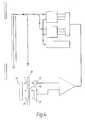
- Figure 4 is likewise a modification of Figure 2, and like figure 3, has second and third reference pixels 19,20, the second 19 being always hard ON, the third 20 being always hard OFF.
- Additional reference pixels are preferably, but not necessarily, constructed in the same auxiliary LCD panel as the first reference pixel. Operation is otherwise the same as the embodiment of Figure 3.
- the embodiment of Figure 5 is a modification of Figure 3.
- the light source 8 of Figure 3 is not used; instead the ambient light incident on the front of the display is allowed to pass through the first, second and third reference elements. Otherwise operation is identical with the Figure 3 embodiment.
Landscapes
- Engineering & Computer Science (AREA)
- Chemical & Material Sciences (AREA)
- Crystallography & Structural Chemistry (AREA)
- Physics & Mathematics (AREA)
- Computer Hardware Design (AREA)
- General Physics & Mathematics (AREA)
- Theoretical Computer Science (AREA)
- Liquid Crystal (AREA)
- Liquid Crystal Display Device Control (AREA)
- Control Of Indicators Other Than Cathode Ray Tubes (AREA)
Abstract
Description
- This invention relates to liquid crystal displays.
- Liquid crystal displays (LCDs) may be either directly driven or multiplexed. In directly driven LCDs, each segment or element has its own driver. In multiplexed LCDs, one driver drives a number of elements. For multiplexed LCDs having large numbers of elements, a matrix arrangement is commonly used, the matrix consisting of rows and columns of conductors having elements disposed at the intersection of each row and column conductor. The row and column conductors are energised by multiple level driving waveforms. The voltage levels of the waveforms are chosen according to the upper and lower transmission voltage threshold values of the liquid crystal and are conveniently generated by a resistive potential divider. This allows the voltage levels to be adjusted in step with each other by adjusting the voltage which is applied across the potential divider, e.g. by hand tuning. Such adjustment is required for initially setting up the display. Temperature-compensated. LCDs are known, in which a temperature - dependent voltage source is included having a linear temperature - voltage characteristic. Such temperature compensation gives acceptable performance over a limited temperature range, for example -5 to +45°C. If it is desired to operate over a wider range, it would be possible in principle to produce a voltage source having a non-linear temperature characteristic matching that of the display, but such a source would be considerably more complex and expensive than one having a linear characteristic, and would require calibration over the temperature range.
- Another disadvantage of a temperature - controlled voltage source is that the temperature - responsive element is in general somewhat remote from the display panel and has a different time - response under rapid changes of temperature. This means that until the temperature has stabilised, the contrast and legibility of the display will be degraded.
- Proposals have been made to control the brightness and/or contrast of an LCD by measuring the transmissivity of a control element of the LCD using a light sensor whose output is utilised to determine the drive signals applied to the control element and to the other elements of the LCD.
- Japanese Patent Application JP 59195627 shows an arrangement in which a control element is energised so as to have a transmissivity of 50%, ie mid-way between the Hard-ON and Hard-OFF states. As the transmissivity varies with temperature etc, so the drive waveform is varied to maintain the transmissivity at the 50% level.
- European Patent Application EP 0313331 discloses an arrangement for maintaining the grey scale characteristics of an LCD constant over a range of temperatures. A control element is successively energised with drive waveforms corresponding to points on the grey scale and the measured transmissivity at each point is utilised to ensure that the correct grey scale waveforms are supplied to the display.
- These prior art arrangements necessitate the generation of waveforms necessary to put their respective control elements into states intermediate the Hard-ON and Hard-OFF states. The present invention arose from an attempt to provide an improved liquid crystal display.
- In accordance with the invention, a liquid crystal display (LCD) comprising a plurality of liquid crystal elements; means for applying voltages across the elements; photodetector means to detect transmissivity of an element; means for adjusting the voltages applied across the elements in dependence on the transmissivity detected, means to repetitively switch the said element between a first state in which it exhibits a first level of transmissivity and a second state in which it exhibits a second level of transmissivity lower than the first level; is characterised in that the means for adjusting comprises means for comparing the mean output signal of the photodetector means with a reference value representative of a desired mean transmissivity level corresponding to the mean of the first and second levels, and means for producing the reference value whereby the mean transmissivity of the LCD elements is maintained at the desired level.
- The use of one of the elements of the display as a reference element, and the measurement of its actual transmissivity allows pre-selected optical properties e.g. contrast to be maintained even if there are changes in the physical condition of the material of the element e.g. due to temperature or ageing.
- Voltages may be adjusted to obtain desired contrast or desired brightness.
- The LCD may include a light source to provide a reference illumination of the element, and the photo-detector may be arranged to detect the intensity of the light source retro-reflected through the element.
- Preferred embodiments of the invention will now be described by way of example with reference to the accompanying drawings in which:
- Figure 1 shows a first embodiment of the invention in which a multiplexed LCD display has a reference cell constructed as an integral part of the display;
- Figure 2 shows a second embodiment utilising a discrete reference cell;
- Figure 3 shows a third embodiment which is a modification of Figure 1 in which a reference level is determined automatically;
- Figure 4 shows a fourth embodiment which is a modification of Figure 2 in which the reference level is determined automatically.
- Figure 5 shows a fifth embodiment which is a modification of Figure 3.
- Figure 1 shows multiplexed Super Birefringent Effect (SBE) Liquid Crystal Display (LCD) comprising a matrix
LCD display panel 2 having a main array of pixels which operate in the standard transflective or reflective mode in conjunction with either a rear mounted transflector and backlight, or a rear mountedreflector 4. Acontrol pixel 1 is eclipsed from main view by the bezel and has a front mountedreflector 9. Thecontrol pixel 1 is substantially identical with the pixels of the main display. The control pixel is illuminated from the rear by alight source 8 such as a LED. Light from the light source passes through thecontrol pixel 1, is reflected by the reflector back through the control pixel and falls on aphotodetector 10. Thecontrol pixel 1 is driven alternately n fields on and m fields off by a spare row/column combination of the main horizontal 5 and vertical 6 LCD drive circuits. This is achieved by suitably programming the system control micro-computer 7. It is necessary to drive thecontrol pixel 1 such that no DC bias be allowed to accrue across it. - The arithmetic mean of the output signal from the
photodetector 10 is compared with a reference signal from areference signal source 11 using a DC coupled Miller integrator-type comparator 12, the time constant-determining components of which are selected such as to effect satisfactory integration over the period of n + m fields. The reference signal is chosen so as to correspond with the desired transmission of the control pixel and hence of the main display. - The output signal of the comparator is applied to the
resistor chain 13 which generates the reference voltages for the horizontal andvertical driver circuits - To provide optimum contrast, the control pixel is driven such that m = n = 2, i.e. 2 fields on, and 2 fields off, and the reference signal is chosen so as to correspond with 50% transmission of the control pixel, and hence of the main display. This feedback ensures that V on and V off are always maintained at values which produce optimum contrast, even at extremes of temperature. This is because, although the temperature/voltage characteristics are non-linear at temperature extremes, the V on and V off voltages maintain their relationship relative to the 50% transmission voltage.
- Under certain circumstances it may be advantageous to increase or decrease the absolute brightness of the display, even though this means departure from the optimum contrast. This can be done by changing the values of m and n such that the ratio between the ON time and the OFF time of the control pixel is varied, the reference value remaining constant. n and m are changed by reprogramming the microcomputer, which is easily done and requires no additional electrical connections. It also allows the brightness of the display to be controlled remotely, using a databus to reprogramme the microcomputer.
- Illumination of the reference pixel and monitoring of its transmission may be effected by pulsed operation, for example 100 .s per field, in applications where power consumption is critical. Sample and hold techniques are advantageously employed in such arrangements.
- In the embodiment of Figure 1, as the reference pixel is an integral part of the display, accurate stabilisation of contrast or absolute illumination will be maintained under forced heating or cooling of the display, and for variations in the properties of the liquid crystal itself.
- A second embodiment of the invention is shown in Figure 2. The main difference between this and Figure 1 is that the reference pixel is not an integral part of the main display, but forms part of an
auxiliary LCD panel 14. The auxiliary LCD panel is made of the same material and has identical electrical and optical properties as the main display. Such an arrangement allows thephotodetector 15 and thelight source 16 to be placed on opposite sides of the auxiliary panel so as to operate the reference pixel in the transmission mode. Otherwise, operation is identical to the Figure 1 embodiment. - The embodiment of figure 3, shows a modification of the Figure 1 embodiment in which the reference voltage is generated automatically. The
reference voltage source 11 is replaced by second andthird reference pixels second photodetector 17. Thesecond reference pixel 19 is driven so as to be always hard ON, while thethird reference pixel 20 is driven so as to be always hard OFF e.g. by applying zero volts across it. Light, which is conveniently obtained from thesame light source 8 as that which illuminates thefirst reference pixel 1, is passed through the second and third reference pixels and falls on thesecond photodetector 17, which is preferably matched to thefirst photodetector 10. The second detector thus produces an output signal proportional to the sum of the best ON transmissivity and the best OFF transmissivity. It can be adjusted to give the desired reference value, namely half the sum of the ON transmissivity and the OFF transmissivity, by any convenient means. For example, the second and third reference pixels may each be constructed so as to have half the area of the first reference pixel, thesecond photosensor 17 may be half the area of thefirst photosensor 10, or the Millerintegrator comparator 12 may include scaling circuitry e.g. a potential divider to reduce the value of the signal applied to it from the second photo sensor. - This arrangement is particularly advantageous as it requires no setting up or adjustment, even when different types of liquid crystal are used, the reference value always being set to give the optimum value for the particular liquid crystal being used.
- The embodiment of Figure 4 is likewise a modification of Figure 2, and like figure 3, has second and
third reference pixels - These additional reference pixels are preferably, but not necessarily, constructed in the same auxiliary LCD panel as the first reference pixel. Operation is otherwise the same as the embodiment of Figure 3.
- The embodiment of Figure 5 is a modification of Figure 3. In this embodiment, the
light source 8 of Figure 3 is not used; instead the ambient light incident on the front of the display is allowed to pass through the first, second and third reference elements. Otherwise operation is identical with the Figure 3 embodiment. - While the description refers to light, this is not restricted to visible light, but also encompasses non-visible light e.g. ultra-violet and infra-red.
- Further, while the invention has been described with particular reference to a matrix array, the invention is not restricted to the particular embodiments described. It is equally applicable to multiplexed LCDs in the form of alphanumeric displays, and indicators, or to non-multiplexed LCDs.
Claims (16)
- A liquid crystal display (LCD) (2)comprising a plurality of liquid crystal elements; means (5,6,7,13)for applying voltages across the elements; photodetector means (10;15)to detect transmissivity of an element (1;14); means (7,11,12)for adjusting the voltages applied across the elements in dependence on the transmissivity detected, means (5,6,7)to repetitively switch the said element (1;14)between a first state in which it exhibits a first level of transmissivity and a second state in which it exhibits a second level of transmissivity lower than the first level; characterised in that the means for adjusting comprises means (12)for comparing the mean output signal of the photodetector means (10;15)with a reference value representative of a desired mean transmissivity level corresponding to the mean of the first and second levels, and means (11; 17,19,20; 16,17,19,20)for producing the reference value whereby the mean transmissivity of the LCD elements is maintained at the desired level.
- A liquid crystal display as claimed in Claim 1 in which the elements are arranged such that respective first electrodes of a number of elements are coupled to a single driver stage such that all elements are individually addressable.
- A liquid crystal display as claimed in Claim 2 in which the elements are disposed in a matrix of rows and columns.
- A liquid crystal display as claimed in any one of Claims 1 to 3 in which the output signal of the photodetector (10;15) represents the actual mean transmissivity level.
- A liquid crystal display as claimed in Claim 4 in which the means for producing the reference value comprises first and second reference element means (19,20), and further photodetector means (17), the first reference element means (19) being maintained in the first level of transmissivity, the second reference element means (20) being maintained in the second level of transmissivity, the further photodetector means (17) being coupled to the first and second reference elements (19,20) so as to produce a signal representing the mean transmissivity of the first and second elements; the signal so produced comprising the said reference value.
- A liquid crystal display as claimed in any of Claims 1-5 in which the said element is illuminated in reflective mode by a light source (8) disposed on the same side of the LCD display panel as the said photodetector means.
- A liquid crystal display as claimed in any of Claims 1-5 in which the said element (1) is illuminated in transmissive mode by a light source (16) disposed on the opposite side of the display panel from the said photodetector means.
- A liquid crystal display as claimed in Claim 5 in which the first and second reference elements (19,20) are illuminated in reflective mode by a light source (8) disposed on the same side of the LCD display panel as the said photodetector means.
- A liquid crystal display as claimed in Claim 5 in which the said element (1) and the first and second reference elements (19,20) are illuminated in transmissive mode by a light source (16) disposed on the opposite side of the LCD display panel as the said photodetector means.
- A liquid crystal display as claimed in any preceding claim in which the means to adjust is arranged to adjust the mean transmissivity of the LCD elements in order to obtain desired visual properties.
- A liquid crystal display as claimed in Claim 10 in which, the means to adjust is arranged to adjust the mean transmissivity such as to provide maximum contrast of the display.
- A liquid crystal display as claimed in Claim 11 in which the time for which the said element is in the first state and the time for which the said element is in the second state, are independently adjustable.
- A liquid crystal display as claimed in Claim 11 in which the time for which the said element is in the first state is arranged to be substantially the same as the time for which the said element is in the second state.
- A liquid crystal display as claimed in Claim 10 in which the means to adjust is arranged to adjust the mean transmissivity so as to adjust the absolute brightness of the display.
- A liquid crystal display as claimed in Claim 14 in which the absolute level of brightness of the display is adjusted by altering the relationship between the time for which the said element (1) is in the first state and the time for which the said element (1) is in the second state.
- A liquid crystal display as claimed in Claim 15 and comprising a microcomputer (7) to produce signals which determine the switching of the elements of the liquid crystal display between first and second states, in which the time relationship between the first and second states of the said elements is varied by reprogramming the microcomputer.
Applications Claiming Priority (2)
| Application Number | Priority Date | Filing Date | Title |
|---|---|---|---|
| GB8924221 | 1989-10-27 | ||
| GB8924221A GB2237400B (en) | 1989-10-27 | 1989-10-27 | Control of liquid crystal display visual properties |
Publications (3)
| Publication Number | Publication Date |
|---|---|
| EP0425210A2 EP0425210A2 (en) | 1991-05-02 |
| EP0425210A3 EP0425210A3 (en) | 1992-08-19 |
| EP0425210B1 true EP0425210B1 (en) | 1995-08-23 |
Family
ID=10665273
Family Applications (1)
| Application Number | Title | Priority Date | Filing Date |
|---|---|---|---|
| EP90311528A Expired - Lifetime EP0425210B1 (en) | 1989-10-27 | 1990-10-19 | Control of liquid crystal display visual properties |
Country Status (6)
| Country | Link |
|---|---|
| US (1) | US5157525A (en) |
| EP (1) | EP0425210B1 (en) |
| JP (1) | JPH03179318A (en) |
| AT (1) | ATE126916T1 (en) |
| DE (1) | DE69021825T2 (en) |
| GB (1) | GB2237400B (en) |
Families Citing this family (56)
| Publication number | Priority date | Publication date | Assignee | Title |
|---|---|---|---|---|
| FR2652434A1 (en) * | 1989-09-22 | 1991-03-29 | Sextant Avionique | METHOD AND DEVICE FOR OPTIMIZING THE CONTRAST AND THE ANGLE OF VIEW OF A LIQUID CRYSTAL DISPLAY |
| GB9024978D0 (en) * | 1990-11-16 | 1991-01-02 | Rank Cintel Ltd | Digital mirror spatial light modulator |
| GB9115401D0 (en) * | 1991-07-17 | 1991-09-04 | Philips Electronic Associated | Matrix display device and its method of operation |
| US5206633A (en) * | 1991-08-19 | 1993-04-27 | International Business Machines Corp. | Self calibrating brightness controls for digitally operated liquid crystal display system |
| US5245326A (en) * | 1991-08-19 | 1993-09-14 | International Business Machines Corp. | Calibration apparatus for brightness controls of digitally operated liquid crystal display system |
| GB9125331D0 (en) * | 1991-11-28 | 1992-01-29 | Shaye Communications Ltd | Illumination of displays |
| JP3241432B2 (en) * | 1992-05-22 | 2001-12-25 | パイオニア株式会社 | Photoconductive liquid crystal light valve display with temperature change detection function |
| JP2818335B2 (en) * | 1992-05-22 | 1998-10-30 | シャープ株式会社 | Liquid crystal device, display device, photodetector, color copier, printing plate making device, image input / output device, image operation device, lighting device, and method of manufacturing liquid crystal device |
| GB9211283D0 (en) * | 1992-05-28 | 1992-07-15 | Philips Electronics Uk Ltd | Liquid crystal display devices |
| US5548420A (en) * | 1993-03-16 | 1996-08-20 | Fuji Xerox Co., Ltd. | Liquid-crystal display device and method for both displaying fast moving images and holding static images |
| JPH07230078A (en) * | 1993-12-20 | 1995-08-29 | Kansei Corp | Liquid crystal display device |
| US6115021A (en) * | 1994-07-04 | 2000-09-05 | Sharp Kabushiki Kaisha | Method and apparatus for driving a liquid crystal panel using a ferroelectric liquid crystal material having a negative dielectric anisotropy |
| US6204834B1 (en) * | 1994-08-17 | 2001-03-20 | Si Diamond Technology, Inc. | System and method for achieving uniform screen brightness within a matrix display |
| US5636041A (en) * | 1995-05-24 | 1997-06-03 | Dell Usa, L.P. | Technique for increasing the visibility of an LCD panel during warm-up thereof |
| US5760760A (en) * | 1995-07-17 | 1998-06-02 | Dell Usa, L.P. | Intelligent LCD brightness control system |
| JP2771499B2 (en) * | 1995-12-19 | 1998-07-02 | 静岡日本電気株式会社 | Individually selected call receiver with display |
| GB2312121A (en) * | 1996-04-13 | 1997-10-15 | Thomson Multimedia Sa | LCD television projector with lamp aging compensation |
| US5786801A (en) * | 1996-09-06 | 1998-07-28 | Sony Corporation | Back light control apparatus and method for a flat display system |
| US5914764A (en) * | 1996-09-25 | 1999-06-22 | Rockwell International Corporation | Method and apparatus for using optical response time to control a liquid crystal display |
| DE19710503A1 (en) * | 1997-03-13 | 1998-10-29 | Siemens Ag | Optical display device for telephone devices |
| JP3317871B2 (en) * | 1997-03-27 | 2002-08-26 | シャープ株式会社 | Display device |
| US6496176B1 (en) * | 1997-12-05 | 2002-12-17 | Citizen Watch Co., Ltd. | Liquid crystal device and method for driving the same |
| GB9904704D0 (en) * | 1999-03-03 | 1999-04-21 | Secr Defence | Addressing bistable nematic liquid crystal devices |
| DE10023147A1 (en) * | 2000-05-12 | 2001-11-15 | Mannesmann Vdo Ag | Method for regulating at least one parameter of a liquid crystal cell and liquid crystal cell controllable by such a method |
| EP1158483A3 (en) * | 2000-05-24 | 2003-02-05 | Eastman Kodak Company | Solid-state display with reference pixel |
| JP2002162934A (en) * | 2000-09-29 | 2002-06-07 | Eastman Kodak Co | Flat-panel display with luminance feedback |
| US6320325B1 (en) | 2000-11-06 | 2001-11-20 | Eastman Kodak Company | Emissive display with luminance feedback from a representative pixel |
| KR100381423B1 (en) * | 2001-07-23 | 2003-04-26 | 삼성전자주식회사 | portable computer and controlling method thereof |
| US6836260B2 (en) * | 2001-07-31 | 2004-12-28 | Eastman Kodak Company | Light emitting flat-panel display |
| US20040254716A1 (en) * | 2001-09-10 | 2004-12-16 | Masumitsu Ino | Car-mounted display and car navigation system |
| KR100438827B1 (en) * | 2001-10-31 | 2004-07-05 | 삼성전기주식회사 | Method for improving gradation of image, and image display apparatus for performing the method |
| US7012590B2 (en) * | 2001-11-23 | 2006-03-14 | Aiptek International Inc. | Motionless-image display with auto-adjusting light system and the method for forming the same |
| US20030206163A1 (en) * | 2001-12-31 | 2003-11-06 | Yew-Peng Kee | LCD with photo-detecting capability and control method thereof |
| US6720942B2 (en) | 2002-02-12 | 2004-04-13 | Eastman Kodak Company | Flat-panel light emitting pixel with luminance feedback |
| US6870529B1 (en) | 2002-03-28 | 2005-03-22 | Ncr Corporation | System and method for adjusting display brightness levels according to user preferences |
| EP1355289B1 (en) * | 2002-04-15 | 2008-07-02 | Pioneer Corporation | Drive unit of self-luminous device with degradation detection function |
| JP4808913B2 (en) * | 2003-04-08 | 2011-11-02 | グローバル・オーエルイーディー・テクノロジー・リミテッド・ライアビリティ・カンパニー | Display device |
| US20070247416A1 (en) * | 2003-05-14 | 2007-10-25 | Au Optronics Corp. | Transflective liquid crystal display device and method of fabricating the same |
| TWI229764B (en) * | 2003-05-14 | 2005-03-21 | Au Optronics Corp | A transflective liquid crystal display device |
| JP2004361618A (en) * | 2003-06-04 | 2004-12-24 | Hitachi Displays Ltd | Liquid crystal display |
| WO2004111984A1 (en) * | 2003-06-19 | 2004-12-23 | Koninklijke Philips Electronics N.V. | Display system with impending failure indicator |
| US7023313B2 (en) * | 2003-07-16 | 2006-04-04 | Marvell World Trade Ltd. | Power inductor with reduced DC current saturation |
| US20050104821A1 (en) * | 2003-11-14 | 2005-05-19 | Nokia Corporation | Display arrangement |
| US20050253777A1 (en) * | 2004-05-12 | 2005-11-17 | E Ink Corporation | Tiled displays and methods for driving same |
| CN100351886C (en) * | 2004-06-30 | 2007-11-28 | 友达光电股份有限公司 | Display brightness compensation device, organic light emitting diode display and compensation method thereof |
| KR20070083352A (en) * | 2006-02-21 | 2007-08-24 | 삼성전자주식회사 | Display device and driving method thereof |
| EP1879172A1 (en) * | 2006-07-14 | 2008-01-16 | Barco NV | Aging compensation for display boards comprising light emitting elements |
| EP1879169A1 (en) | 2006-07-14 | 2008-01-16 | Barco N.V. | Aging compensation for display boards comprising light emitting elements |
| WO2008017315A1 (en) * | 2006-08-08 | 2008-02-14 | Gm Global Technology Operations, Inc. | Image reproducing device and operating method therefore |
| KR100872352B1 (en) * | 2006-11-28 | 2008-12-09 | 한국과학기술원 | Data driving circuit and organic light emitting display device including the same |
| TW200837697A (en) * | 2007-03-07 | 2008-09-16 | Tpo Displays Corp | Comparator and image display system |
| KR20080101680A (en) * | 2007-05-18 | 2008-11-21 | 가부시키가이샤 한도오따이 에네루기 켄큐쇼 | Liquid crystal display device, electronic device, and driving method thereof |
| TWI341406B (en) * | 2007-07-23 | 2011-05-01 | Au Optronics Corp | Diaply panel and its application |
| US7960682B2 (en) | 2007-12-13 | 2011-06-14 | Apple Inc. | Display device control based on integrated ambient light detection and lighting source characteristics |
| EP2159783A1 (en) * | 2008-09-01 | 2010-03-03 | Barco N.V. | Method and system for compensating ageing effects in light emitting diode display devices |
| JP2010266859A (en) * | 2010-04-14 | 2010-11-25 | Hitachi Displays Ltd | Liquid crystal display |
Family Cites Families (24)
| Publication number | Priority date | Publication date | Assignee | Title |
|---|---|---|---|---|
| CH520937A (en) * | 1970-05-27 | 1972-03-31 | Bbc Brown Boveri & Cie | Arrangement for displaying an electrical measurement voltage by means of a display medium extending over a large area between two electrodes |
| US3770961A (en) * | 1972-11-24 | 1973-11-06 | Baird Atomic Inc | Liquid crystal imaging system |
| US4119842A (en) * | 1977-06-17 | 1978-10-10 | General Motors Corporation | Heater control system for liquid crystal device |
| JPS5481879A (en) * | 1977-12-12 | 1979-06-29 | Seiko Instr & Electronics Ltd | Electronic watch |
| GB2042238B (en) * | 1979-02-14 | 1982-12-08 | Matsushita Electric Industrial Co Ltd | Drive circuit for a liquid crystal display panel |
| JPS5639523A (en) * | 1979-09-10 | 1981-04-15 | Hitachi Ltd | Liquid crystal display device |
| JPS5685792A (en) * | 1979-12-14 | 1981-07-13 | Citizen Watch Co Ltd | Liquid crystal display unit |
| US4603946A (en) * | 1982-09-29 | 1986-08-05 | Kabushiki Kaisha Tokai Rika Denki Seisakusho | Reflection controllable view mirror device for motor vehicle or the like |
| US4690508A (en) * | 1982-12-15 | 1987-09-01 | C-D Marketing, Ltd. | Liquid crystal closed-loop controlled mirror systems |
| JPS59195627A (en) * | 1983-04-21 | 1984-11-06 | Olympus Optical Co Ltd | Liquid crystal display device |
| US4775891A (en) * | 1984-08-31 | 1988-10-04 | Casio Computer Co., Ltd. | Image display using liquid crystal display panel |
| US4795248A (en) * | 1984-08-31 | 1989-01-03 | Olympus Optical Company Ltd. | Liquid crystal eyeglass |
| US4825201A (en) * | 1985-10-01 | 1989-04-25 | Mitsubishi Denki Kabushiki Kaisha | Display device with panels compared to form correction signals |
| JPS62125329A (en) * | 1985-11-27 | 1987-06-06 | Hosiden Electronics Co Ltd | Transmission type display device |
| US4738514A (en) * | 1986-01-16 | 1988-04-19 | Rca Corporation | Crystal variation compensation circuit for liquid crystal displays |
| JPS62246014A (en) * | 1986-04-18 | 1987-10-27 | Fujitsu Ltd | Liquid crystal display device |
| DE3634508C1 (en) * | 1986-10-09 | 1988-06-16 | Rupert Fuerthbauer | Optical filter with automatic control of the optical transmission |
| JPS6398636A (en) * | 1986-10-16 | 1988-04-30 | Fujitsu Ltd | Method for accommodative driving liquid crystal display device |
| GB2199439B (en) * | 1986-12-10 | 1990-03-28 | Smiths Industries Plc | Display units |
| JP2612267B2 (en) * | 1987-03-31 | 1997-05-21 | キヤノン株式会社 | Display control device |
| JPH07113723B2 (en) * | 1987-06-29 | 1995-12-06 | ホシデン株式会社 | Liquid crystal display |
| US4848877A (en) * | 1987-09-29 | 1989-07-18 | Cambridge Research And Instrumentation, Inc. | Liquid crystal devices and systems using such devices |
| US4888599A (en) * | 1987-10-23 | 1989-12-19 | Rockwell International Corp. | Real time apparatus for adjusting contrast ratio of liquid crystal displays |
| GB2213303B (en) * | 1987-12-02 | 1992-01-08 | Gen Electric Co Plc | Liquid crystal displays |
-
1989
- 1989-10-27 GB GB8924221A patent/GB2237400B/en not_active Expired - Fee Related
-
1990
- 1990-10-19 EP EP90311528A patent/EP0425210B1/en not_active Expired - Lifetime
- 1990-10-19 DE DE69021825T patent/DE69021825T2/en not_active Expired - Fee Related
- 1990-10-19 AT AT90311528T patent/ATE126916T1/en not_active IP Right Cessation
- 1990-10-23 US US07/601,136 patent/US5157525A/en not_active Expired - Fee Related
- 1990-10-25 JP JP2288259A patent/JPH03179318A/en active Pending
Also Published As
| Publication number | Publication date |
|---|---|
| GB2237400B (en) | 1994-04-20 |
| JPH03179318A (en) | 1991-08-05 |
| ATE126916T1 (en) | 1995-09-15 |
| DE69021825T2 (en) | 1996-01-18 |
| EP0425210A3 (en) | 1992-08-19 |
| US5157525A (en) | 1992-10-20 |
| EP0425210A2 (en) | 1991-05-02 |
| GB2237400A (en) | 1991-05-01 |
| GB8924221D0 (en) | 1989-12-13 |
| DE69021825D1 (en) | 1995-09-28 |
Similar Documents
| Publication | Publication Date | Title |
|---|---|---|
| US5157525A (en) | Control of liquid crystal display visual properties to compensate for variation in the characteristics of the liquid crystal | |
| US5914764A (en) | Method and apparatus for using optical response time to control a liquid crystal display | |
| TWI409735B (en) | Approach to adjust driving waveforms for a display device | |
| US8508155B2 (en) | System and method for calibrating backlight devices | |
| US4888599A (en) | Real time apparatus for adjusting contrast ratio of liquid crystal displays | |
| US5093654A (en) | Thin-film electroluminescent display power supply system for providing regulated write voltages | |
| US5162785A (en) | Method and devices for optimizing the contrast and the angle of view of a liquid crystal display | |
| CA2275176C (en) | Common electrode voltage driving circuit for a liquid crystal display | |
| US5936603A (en) | Liquid crystal display with temperature compensated voltage | |
| US7271790B2 (en) | Combined temperature and color-temperature control and compensation method for microdisplay systems | |
| EP1445757B1 (en) | Organic el panel drive circuit | |
| US5245326A (en) | Calibration apparatus for brightness controls of digitally operated liquid crystal display system | |
| KR100502772B1 (en) | Apparatus for providing a nonlinear response | |
| US6211852B1 (en) | Liquid crystal display device | |
| US7385582B2 (en) | Temperature control and compensation method for microdisplay systems | |
| US6362803B1 (en) | Liquid crystal display having adjustable effective voltage value for display | |
| US5589960A (en) | Liquid crystal display system | |
| US7750582B2 (en) | Liquid crystal display device | |
| US5900851A (en) | Electroluminescent panel drive optimization | |
| JPH09292601A (en) | Liquid crystal display device | |
| GB2217089A (en) | Display device | |
| KR920006929B1 (en) | Testing apparatus of display charateristics in liquid crystal display | |
| KR20080027421A (en) | Display | |
| JPH07301784A (en) | Liquid crystal display | |
| KR101027352B1 (en) | Automatic flicker adjustment method of liquid crystal display and automatic adjustment circuit |
Legal Events
| Date | Code | Title | Description |
|---|---|---|---|
| PUAI | Public reference made under article 153(3) epc to a published international application that has entered the european phase |
Free format text: ORIGINAL CODE: 0009012 |
|
| AK | Designated contracting states |
Kind code of ref document: A2 Designated state(s): AT BE CH DE DK ES FR GR IT LI LU NL SE |
|
| K1C3 | Correction of patent application (complete document) published |
Effective date: 19910502 |
|
| PUAL | Search report despatched |
Free format text: ORIGINAL CODE: 0009013 |
|
| AK | Designated contracting states |
Kind code of ref document: A3 Designated state(s): AT BE CH DE DK ES FR GR IT LI LU NL SE |
|
| 17P | Request for examination filed |
Effective date: 19930215 |
|
| 17Q | First examination report despatched |
Effective date: 19940801 |
|
| GRAA | (expected) grant |
Free format text: ORIGINAL CODE: 0009210 |
|
| AK | Designated contracting states |
Kind code of ref document: B1 Designated state(s): AT BE CH DE DK ES FR GR IT LI LU NL SE |
|
| PG25 | Lapsed in a contracting state [announced via postgrant information from national office to epo] |
Ref country code: IT Free format text: LAPSE BECAUSE OF FAILURE TO SUBMIT A TRANSLATION OF THE DESCRIPTION OR TO PAY THE FEE WITHIN THE PRESCRIBED TIME-LIMIT;WARNING: LAPSES OF ITALIAN PATENTS WITH EFFECTIVE DATE BEFORE 2007 MAY HAVE OCCURRED AT ANY TIME BEFORE 2007. THE CORRECT EFFECTIVE DATE MAY BE DIFFERENT FROM THE ONE RECORDED. Effective date: 19950823 Ref country code: AT Effective date: 19950823 Ref country code: DK Effective date: 19950823 Ref country code: GR Free format text: LAPSE BECAUSE OF FAILURE TO SUBMIT A TRANSLATION OF THE DESCRIPTION OR TO PAY THE FEE WITHIN THE PRESCRIBED TIME-LIMIT Effective date: 19950823 Ref country code: FR Free format text: THE PATENT HAS BEEN ANNULLED BY A DECISION OF A NATIONAL AUTHORITY Effective date: 19950823 Ref country code: BE Effective date: 19950823 Ref country code: ES Free format text: THE PATENT HAS BEEN ANNULLED BY A DECISION OF A NATIONAL AUTHORITY Effective date: 19950823 Ref country code: NL Free format text: LAPSE BECAUSE OF NON-PAYMENT OF DUE FEES Effective date: 19950823 |
|
| REF | Corresponds to: |
Ref document number: 126916 Country of ref document: AT Date of ref document: 19950915 Kind code of ref document: T |
|
| REF | Corresponds to: |
Ref document number: 69021825 Country of ref document: DE Date of ref document: 19950928 |
|
| PG25 | Lapsed in a contracting state [announced via postgrant information from national office to epo] |
Ref country code: LU Free format text: LAPSE BECAUSE OF NON-PAYMENT OF DUE FEES Effective date: 19951031 |
|
| PGFP | Annual fee paid to national office [announced via postgrant information from national office to epo] |
Ref country code: CH Payment date: 19951031 Year of fee payment: 6 |
|
| REG | Reference to a national code |
Ref country code: CH Ref legal event code: PL |
|
| PG25 | Lapsed in a contracting state [announced via postgrant information from national office to epo] |
Ref country code: SE Effective date: 19951123 |
|
| EN | Fr: translation not filed | ||
| NLV1 | Nl: lapsed or annulled due to failure to fulfill the requirements of art. 29p and 29m of the patents act | ||
| PLBE | No opposition filed within time limit |
Free format text: ORIGINAL CODE: 0009261 |
|
| STAA | Information on the status of an ep patent application or granted ep patent |
Free format text: STATUS: NO OPPOSITION FILED WITHIN TIME LIMIT |
|
| PG25 | Lapsed in a contracting state [announced via postgrant information from national office to epo] |
Ref country code: DE Effective date: 19960702 |
|
| 26N | No opposition filed | ||
| PG25 | Lapsed in a contracting state [announced via postgrant information from national office to epo] |
Ref country code: CH Free format text: LAPSE BECAUSE OF FAILURE TO SUBMIT A TRANSLATION OF THE DESCRIPTION OR TO PAY THE FEE WITHIN THE PRESCRIBED TIME-LIMIT Effective date: 19961031 Ref country code: LI Free format text: LAPSE BECAUSE OF FAILURE TO SUBMIT A TRANSLATION OF THE DESCRIPTION OR TO PAY THE FEE WITHIN THE PRESCRIBED TIME-LIMIT Effective date: 19961031 |