EP0424174A2 - Production of images using an array of light emitting diodes - Google Patents
Production of images using an array of light emitting diodes Download PDFInfo
- Publication number
- EP0424174A2 EP0424174A2 EP90311514A EP90311514A EP0424174A2 EP 0424174 A2 EP0424174 A2 EP 0424174A2 EP 90311514 A EP90311514 A EP 90311514A EP 90311514 A EP90311514 A EP 90311514A EP 0424174 A2 EP0424174 A2 EP 0424174A2
- Authority
- EP
- European Patent Office
- Prior art keywords
- light emitting
- emitting diodes
- array
- detector
- exposure
- Prior art date
- Legal status (The legal status is an assumption and is not a legal conclusion. Google has not performed a legal analysis and makes no representation as to the accuracy of the status listed.)
- Granted
Links
- 238000004519 manufacturing process Methods 0.000 title description 3
- 239000000463 material Substances 0.000 claims abstract description 21
- 238000005259 measurement Methods 0.000 claims abstract description 21
- 230000003595 spectral effect Effects 0.000 claims abstract description 18
- 238000000034 method Methods 0.000 claims abstract description 11
- 238000001228 spectrum Methods 0.000 description 12
- 238000003384 imaging method Methods 0.000 description 8
- 238000012937 correction Methods 0.000 description 7
- 230000000694 effects Effects 0.000 description 6
- 230000035945 sensitivity Effects 0.000 description 4
- XUIMIQQOPSSXEZ-UHFFFAOYSA-N Silicon Chemical compound [Si] XUIMIQQOPSSXEZ-UHFFFAOYSA-N 0.000 description 3
- 230000005540 biological transmission Effects 0.000 description 3
- 230000003287 optical effect Effects 0.000 description 3
- 229910052710 silicon Inorganic materials 0.000 description 3
- 239000010703 silicon Substances 0.000 description 3
- 238000000295 emission spectrum Methods 0.000 description 2
- 230000001419 dependent effect Effects 0.000 description 1
- 238000006073 displacement reaction Methods 0.000 description 1
- 238000011065 in-situ storage Methods 0.000 description 1
- 238000000691 measurement method Methods 0.000 description 1
- 230000003278 mimic effect Effects 0.000 description 1
- 238000005065 mining Methods 0.000 description 1
- 230000002277 temperature effect Effects 0.000 description 1
- 230000001052 transient effect Effects 0.000 description 1
Images


Classifications
-
- G—PHYSICS
- G03—PHOTOGRAPHY; CINEMATOGRAPHY; ANALOGOUS TECHNIQUES USING WAVES OTHER THAN OPTICAL WAVES; ELECTROGRAPHY; HOLOGRAPHY
- G03B—APPARATUS OR ARRANGEMENTS FOR TAKING PHOTOGRAPHS OR FOR PROJECTING OR VIEWING THEM; APPARATUS OR ARRANGEMENTS EMPLOYING ANALOGOUS TECHNIQUES USING WAVES OTHER THAN OPTICAL WAVES; ACCESSORIES THEREFOR
- G03B17/00—Details of cameras or camera bodies; Accessories therefor
-
- H—ELECTRICITY
- H04—ELECTRIC COMMUNICATION TECHNIQUE
- H04N—PICTORIAL COMMUNICATION, e.g. TELEVISION
- H04N1/00—Scanning, transmission or reproduction of documents or the like, e.g. facsimile transmission; Details thereof
- H04N1/40—Picture signal circuits
- H04N1/40025—Circuits exciting or modulating particular heads for reproducing continuous tone value scales
- H04N1/4005—Circuits exciting or modulating particular heads for reproducing continuous tone value scales with regulating circuits, e.g. dependent upon ambient temperature or feedback control
-
- G—PHYSICS
- G06—COMPUTING; CALCULATING OR COUNTING
- G06K—GRAPHICAL DATA READING; PRESENTATION OF DATA; RECORD CARRIERS; HANDLING RECORD CARRIERS
- G06K15/00—Arrangements for producing a permanent visual presentation of the output data, e.g. computer output printers
- G06K15/02—Arrangements for producing a permanent visual presentation of the output data, e.g. computer output printers using printers
- G06K15/12—Arrangements for producing a permanent visual presentation of the output data, e.g. computer output printers using printers by photographic printing, e.g. by laser printers
- G06K15/1238—Arrangements for producing a permanent visual presentation of the output data, e.g. computer output printers using printers by photographic printing, e.g. by laser printers simultaneously exposing more than one point
- G06K15/1242—Arrangements for producing a permanent visual presentation of the output data, e.g. computer output printers using printers by photographic printing, e.g. by laser printers simultaneously exposing more than one point on one main scanning line
- G06K15/1247—Arrangements for producing a permanent visual presentation of the output data, e.g. computer output printers using printers by photographic printing, e.g. by laser printers simultaneously exposing more than one point on one main scanning line using an array of light sources, e.g. a linear array
-
- H—ELECTRICITY
- H04—ELECTRIC COMMUNICATION TECHNIQUE
- H04N—PICTORIAL COMMUNICATION, e.g. TELEVISION
- H04N1/00—Scanning, transmission or reproduction of documents or the like, e.g. facsimile transmission; Details thereof
- H04N1/40—Picture signal circuits
- H04N1/40025—Circuits exciting or modulating particular heads for reproducing continuous tone value scales
- H04N1/40031—Circuits exciting or modulating particular heads for reproducing continuous tone value scales for a plurality of reproducing elements simultaneously
-
- H—ELECTRICITY
- H04—ELECTRIC COMMUNICATION TECHNIQUE
- H04N—PICTORIAL COMMUNICATION, e.g. TELEVISION
- H04N1/00—Scanning, transmission or reproduction of documents or the like, e.g. facsimile transmission; Details thereof
- H04N1/40—Picture signal circuits
- H04N1/401—Compensating positionally unequal response of the pick-up or reproducing head
- H04N1/4015—Compensating positionally unequal response of the pick-up or reproducing head of the reproducing head
Definitions
- This invention relates to the production of images, particularly grey scale images, using an array of light emitting diodes (LEDs) as the exposure source.
- LEDs light emitting diodes
- Electronic image recording apparatus of a type comprising a line exposure array stationed in a light exposing relationship to a photosensitive material and comprising a plurality of linearly spaced apart light emitting diodes are known in the art. Means are generally provided for effecting a relative displacement between the light exposure array and the photosensitive material in a direction transverse to the longitudinal axis of the exposure array so as to effect an exposure of the entire surface of the photosensitive material.
- bi-level imaging and continuous tone (grey-scale) imaging.
- each pixel of the photosensitive media experiences either maximum or zero exposure by an element of the LED bar, and the image comprises dots of maximum optical density on a background of minimum optical density.
- continuous tone imaging requires that each pixel receives an exposure that is continuously variable, or variable over a sufficiently large number of discrete levels so as to mimic continuous variability.
- the latter type of imaging is needed in areas such as high quality colour reproduction, and requires control of the exposure parameters with a degree of precision not achieved in the prior art, involving the solution of problems not hitherto recognised. These include transient turn-on and -off effects, and pixel shape and spacing effects, and also source wavelength variation effects. The latter effects are addressed by the present invention.
- the present invention provides an imaging method in which the LED exposure apparatus is calibrated to take into account the wavelength difference between LED emissions and the spectral sensitivity of the photosensitive medium.
- a method of calibrating an exposure apparatus comprising an array of light emitting diodes to a photosensitive material to be imaged, which method comprises making separate energy measurements of each light emitting diode with a detector through a coloured filter, so that the spectral response of the detector and filter combination matches that of the photosensitive material in the wavelength region of the emission of the light emitting diode and using said energy measurements to modulate each exposure level of the array of light emitting diodes.
- the invention also extends to the use of the calibration method during exposure of the photosensitive material by the array of LEDs, particularly for grey scale imaging, and to exposure apparatus incorporating calibration means comprising the detector and filter and control means to modulate exposure in response to the energy measurements.
- the energy output of each individual element must be measured, and a corresponding correction applied during exposure.
- the energy measured by a photosensor depends on the spectrum of the source and the spectral response of the detector and will be the integral of the product of the two.
- the effective exposure detected by the photosensitive material depends on the LED spectrum and the spectral sensitivity of the photosensitive medium. If all the LEDs in a bar have the same spectrum then there is a constant ratio between the detector measurements and the integrated energy detected by the photosensitive material.
- LED bars typically show wavelength variations of a few nm, which means that photodetector measurements are no longer representative of the exposure seen by the film.
- the arrangement of the invention is to make energy measurements through a coloured filter so that the spectral response of the detector/filter combination matches that of the photosensitive material.
- the detector then detects exactly what is detected by the photosensitive material.
- Measurements of LED energy may be performed at the factory to calibrate a bar initially, but must also be done in situ to automatically re-calibrate the bar during use.
- Photodetectors with filters are preferably built into the machine itself and accordingly the machine will be calibrated only for one particular photosensitive material.
- E (detector/no filter) ⁇ ⁇ D( ⁇ )S( ⁇ )d ⁇ (1) in which: D( ⁇ ) is the spectral response of the detector, S( ⁇ ) is the spectrum of the LED.
- the spectral response of the film is defined in the following way:
- This spectral response can be derived from a wedge spectrum (optical density vs. wavelength) and a D logE curve for the material.
- Figure 1 shows the spectra over the wavelength range 730 nm to 810 nm of three LEDs on a 400 dots per inch (dpi) Hitachi HLB440A bar commercially available from Hitachi. These spectra represent the extremes of variation across the bar; a difference in the peak wavelength of about 10 nm. There are also differences in both the width and shape, of the spectra, such that the peak wavelength is not sufficient to characterise the spectrum of an LED.
- dpi dots per inch
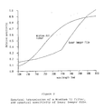
- Figure 2 shows the spectral sensitivity of laser imager film commercially available from Minnesota Mining and Manufacturing Company under the Trade Mark 3M SX560, and the spectral transmission of a Wratten 11 filter.
- the response of a silicon photodiode is fairly flat compared with these two plots.
- the Hitachi LED bar is made up of 32 chips, each with 128 LEDs. It is notable that gross variations can be seen from chip to chip. This is to be expected since the LED spectrum depends principally on the doping levels of the material, and this is likely to be fairly consistent within a chip, but will vary from chip to chip, especially if they are selected from different batches.
- the LEDs whose spectra are shown in Figure 1 are marked on Figure 3.
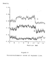
- Figure 4 shows microdensitometer scans of exposed film covering about 256 LEDs, for the three cases of:
- the central block visible in these plots corresponds to LEDs numbers 2432-2559 which have peak wavelengths of about 780 nm, while the LEDs at either end of the plot have peak wavelengths of about 773 nm.
- the spectra of the LEDs of the Hitachi bar were also found to have side peaks in the region of 880 nm which may contribute to film density variations.
- Other LED bars, e.g., Sanyo LPH-13216-07 do not have side peaks in their emission spectra. In order to minimise the problem caused by exposure at different wavelengths it is preferable to use LEDs which have no side peaks in their emission spectra.
- the emission of LEDs may vary with temperature. This variation of emission can contribute to film density variations since the LED bar generally increases in temperature during use and it is difficult to maintain a predetermined constant temperature.
- the temperature effect may be compensated for by making repeated readings to the LEDs at different temperatures and using the data to generate a series of "look-up" tables to provide the necessary exposure correction at each temperature.
- a preferred exposure system includes one or more temperature sensors at the LED bar, look-up tables and associated software to automatically apply any necessary temperature-dependent correction to the exposure time of the LEDs.
Landscapes
- Engineering & Computer Science (AREA)
- Multimedia (AREA)
- Signal Processing (AREA)
- Physics & Mathematics (AREA)
- General Physics & Mathematics (AREA)
- General Engineering & Computer Science (AREA)
- Optics & Photonics (AREA)
- Theoretical Computer Science (AREA)
- Printers Or Recording Devices Using Electromagnetic And Radiation Means (AREA)
- Dot-Matrix Printers And Others (AREA)
- Led Devices (AREA)
- Facsimile Heads (AREA)
- Testing Of Optical Devices Or Fibers (AREA)
- Exposure Or Original Feeding In Electrophotography (AREA)
Abstract
Description
- This invention relates to the production of images, particularly grey scale images, using an array of light emitting diodes (LEDs) as the exposure source.
- Electronic image recording apparatus of a type comprising a line exposure array stationed in a light exposing relationship to a photosensitive material and comprising a plurality of linearly spaced apart light emitting diodes are known in the art. Means are generally provided for effecting a relative displacement between the light exposure array and the photosensitive material in a direction transverse to the longitudinal axis of the exposure array so as to effect an exposure of the entire surface of the photosensitive material.
- One can distinguish two types of imaging using LED bars, namely bi-level imaging and continuous tone (grey-scale) imaging. In the former, each pixel of the photosensitive media experiences either maximum or zero exposure by an element of the LED bar, and the image comprises dots of maximum optical density on a background of minimum optical density. On the other hand, continuous tone imaging requires that each pixel receives an exposure that is continuously variable, or variable over a sufficiently large number of discrete levels so as to mimic continuous variability. The latter type of imaging is needed in areas such as high quality colour reproduction, and requires control of the exposure parameters with a degree of precision not achieved in the prior art, involving the solution of problems not hitherto recognised. These include transient turn-on and -off effects, and pixel shape and spacing effects, and also source wavelength variation effects. The latter effects are addressed by the present invention.
- There are various different arrangements of such image recording apparatus used in bi-level printing applications, which are primarily concerned with obtaining equal energy exposure from each image and eliminating "unexposed lines" in the image caused by the gaps between adjacent LEDs or between rows of LEDs. Examples of such arrangements are disclosed in U.S. Patent Nos. 3,827,062, 4,096,486, 4,435,064 and 4,589,745 and Japanese Patent Application No. 60-175065.
- Whilst the arrangements of the prior art have attempted to control the variation of intensity from LED to LED, the degree of control required for bi-level printing applications is small compared to that required for grey scale imaging where the exposure must be controlled to a precision of 0.5%. The major problem of variation of intensity between separate LEDs can be reduced by measuring these intensities with a photosensor and applying corresponding exposure corrections. However, this does not entirely solve the problem. It has been found that there are often wavelength variations between the emissions of separate LEDs and that such wavelength variations may interact with the film spectral sensitivity to give different effective exposures for the same incident energy.
- The present invention provides an imaging method in which the LED exposure apparatus is calibrated to take into account the wavelength difference between LED emissions and the spectral sensitivity of the photosensitive medium.
- Therefore according to the present invention there is provided a method of calibrating an exposure apparatus comprising an array of light emitting diodes to a photosensitive material to be imaged, which method comprises making separate energy measurements of each light emitting diode with a detector through a coloured filter, so that the spectral response of the detector and filter combination matches that of the photosensitive material in the wavelength region of the emission of the light emitting diode and using said energy measurements to modulate each exposure level of the array of light emitting diodes.
- The invention also extends to the use of the calibration method during exposure of the photosensitive material by the array of LEDs, particularly for grey scale imaging, and to exposure apparatus incorporating calibration means comprising the detector and filter and control means to modulate exposure in response to the energy measurements.
- In order to produce uniform exposure from an LED bar, the energy output of each individual element must be measured, and a corresponding correction applied during exposure. The energy measured by a photosensor depends on the spectrum of the source and the spectral response of the detector and will be the integral of the product of the two. Equally, the effective exposure detected by the photosensitive material depends on the LED spectrum and the spectral sensitivity of the photosensitive medium. If all the LEDs in a bar have the same spectrum then there is a constant ratio between the detector measurements and the integrated energy detected by the photosensitive material. However, LED bars typically show wavelength variations of a few nm, which means that photodetector measurements are no longer representative of the exposure seen by the film.
- The arrangement of the invention is to make energy measurements through a coloured filter so that the spectral response of the detector/filter combination matches that of the photosensitive material. The detector then detects exactly what is detected by the photosensitive material.
- Measurements of LED energy may be performed at the factory to calibrate a bar initially, but must also be done in situ to automatically re-calibrate the bar during use. Photodetectors with filters are preferably built into the machine itself and accordingly the machine will be calibrated only for one particular photosensitive material.
- From a theoretical point of view the energy measured by a bare silicon photodiode is:
E (detector/no filter) = ∫λ D(λ)S(λ)dλ (1)
in which:
D(λ) is the spectral response of the detector,
S(λ) is the spectrum of the LED. - When a filter with a transmission F(λ) is placed over the detector, the measured energy now becomes:
E (detector + filter) =∫λ F(λ)D(λ)S(λ)dλ (2) - The spectral response of the film is defined in the following way:

- This spectral response can be derived from a wedge spectrum (optical density vs. wavelength) and a D logE curve for the material.
- Then the effective energy seen by the film is:
E (film) =∫λ M(λ)S(λ)dλ (4) - The combined filter/detector to measure this effective energy is required, so from equations (2) and (4):
E (detector + filter) = E(film) (5) - Thus, the required spectral transmission of the filter is:
F(λ) =(6)
- The invention will now be described with reference to the accompanying drawings.
- Figure 1 shows the spectra over the
wavelength range 730 nm to 810 nm of three LEDs on a 400 dots per inch (dpi) Hitachi HLB440A bar commercially available from Hitachi. These spectra represent the extremes of variation across the bar; a difference in the peak wavelength of about 10 nm. There are also differences in both the width and shape, of the spectra, such that the peak wavelength is not sufficient to characterise the spectrum of an LED. - In order to prove the principle of the filter measurement method a commercial filter was chosen which provided the closest match to the spectral response of the photographic film. For optimum results a custom filter is required.
- Figure 2 shows the spectral sensitivity of laser imager film commercially available from Minnesota Mining and Manufacturing Company under the Trade Mark 3M SX560, and the spectral transmission of a Wratten 11 filter. The response of a silicon photodiode is fairly flat compared with these two plots.
- Measurements of LED intensity were made both with and without the Wratten filter over the detector. Figure 3 shows the ratio of these two measurements; the variation is entirely due to the filter and reveals the effects of LED spectral variations.
- The Hitachi LED bar is made up of 32 chips, each with 128 LEDs. It is notable that gross variations can be seen from chip to chip. This is to be expected since the LED spectrum depends principally on the doping levels of the material, and this is likely to be fairly consistent within a chip, but will vary from chip to chip, especially if they are selected from different batches. The LEDs whose spectra are shown in Figure 1 are marked on Figure 3.
- Figure 4 shows microdensitometer scans of exposed film covering about 256 LEDs, for the three cases of:
- a) No corrections applied,
- b) Corrections based on measurements with a bare silicon photodiode,
- c) Corrections based on measurements with a photodiode/filter combination.
- The plots have been separated vertically in Figure 4 in the interests of clarity.
- The central block visible in these plots corresponds to LEDs numbers 2432-2559 which have peak wavelengths of about 780 nm, while the LEDs at either end of the plot have peak wavelengths of about 773 nm.
- It is apparent that the bare photodiode measurements have produced some improvement but have by no means eliminated the density variations. The filter measurements however show a distinct improvement.
- The spectra of the LEDs of the Hitachi bar were also found to have side peaks in the region of 880 nm which may contribute to film density variations. Other LED bars, e.g., Sanyo LPH-13216-07 do not have side peaks in their emission spectra. In order to minimise the problem caused by exposure at different wavelengths it is preferable to use LEDs which have no side peaks in their emission spectra.
- In addition to the wavelength variation of emission between individual LEDs it has been found that the emission of LEDs may vary with temperature. This variation of emission can contribute to film density variations since the LED bar generally increases in temperature during use and it is difficult to maintain a predetermined constant temperature. However, the temperature effect may be compensated for by making repeated readings to the LEDs at different temperatures and using the data to generate a series of "look-up" tables to provide the necessary exposure correction at each temperature. A preferred exposure system includes one or more temperature sensors at the LED bar, look-up tables and associated software to automatically apply any necessary temperature-dependent correction to the exposure time of the LEDs.
Claims (5)
Applications Claiming Priority (2)
| Application Number | Priority Date | Filing Date | Title |
|---|---|---|---|
| GB898923709A GB8923709D0 (en) | 1989-10-20 | 1989-10-20 | Production of images using an array of light emmiting diodes |
| GB8923709 | 1989-10-20 |
Publications (3)
| Publication Number | Publication Date |
|---|---|
| EP0424174A2 true EP0424174A2 (en) | 1991-04-24 |
| EP0424174A3 EP0424174A3 (en) | 1992-05-27 |
| EP0424174B1 EP0424174B1 (en) | 1995-09-20 |
Family
ID=10664924
Family Applications (1)
| Application Number | Title | Priority Date | Filing Date |
|---|---|---|---|
| EP90311514A Expired - Lifetime EP0424174B1 (en) | 1989-10-20 | 1990-10-19 | Production of images using an array of light emitting diodes |
Country Status (8)
| Country | Link |
|---|---|
| US (1) | US5051762A (en) |
| EP (1) | EP0424174B1 (en) |
| JP (1) | JP2938956B2 (en) |
| KR (1) | KR910008473A (en) |
| AU (1) | AU629415B2 (en) |
| CA (1) | CA2028051A1 (en) |
| DE (1) | DE69022528T2 (en) |
| GB (1) | GB8923709D0 (en) |
Cited By (7)
| Publication number | Priority date | Publication date | Assignee | Title |
|---|---|---|---|---|
| WO1993004444A1 (en) * | 1991-08-23 | 1993-03-04 | Eastman Kodak Company | Image forming apparatus using high numerical aperture lens and optical fiber |
| WO1993013499A1 (en) * | 1991-12-20 | 1993-07-08 | Siemens Nixdorf Informationssysteme Aktiengesellschaft | Electrographic printer or copier with a device to compensate for the wavelength-dependent light sensitivity of the charge image substrate |
| EP0629905A3 (en) * | 1993-06-14 | 1995-07-19 | Noritsu Koki Co Ltd | Image printer. |
| EP0713328A3 (en) * | 1994-11-16 | 1996-10-16 | Konishiroku Photo Ind | Image forming method for silver halide photographic material |
| US5777723A (en) * | 1993-06-15 | 1998-07-07 | Noritsu Koki Co., Ltd. | Photographic printing apparatus and method |
| EP0965456A1 (en) * | 1998-06-16 | 1999-12-22 | Noritsu Koki Co., Ltd. | Method and apparatus for detecting positions of light emitting elements |
| US6034710A (en) * | 1994-11-16 | 2000-03-07 | Konica Corporation | Image forming method for silver halide photographic material |
Families Citing this family (26)
| Publication number | Priority date | Publication date | Assignee | Title |
|---|---|---|---|---|
| GB9612567D0 (en) * | 1996-06-15 | 1996-08-21 | Kodak Ltd | Scanning of images |
| US6388694B1 (en) * | 1996-12-19 | 2002-05-14 | Minolta Co., Ltd. | Method for calculating the output characteristic of an optical tip array and image forming apparatus |
| US6515693B1 (en) * | 2000-06-29 | 2003-02-04 | Eastman Kodak Company | Calibration station for a printhead adapted to compensate for the wavelength sensitivity of an image recording material |
| KR100399328B1 (en) * | 2000-12-14 | 2003-09-26 | 엘지전자 주식회사 | Steam exhausting apparatus of Dishwasher |
| JP2002325714A (en) * | 2001-03-01 | 2002-11-12 | Sanyo Electric Co Ltd | Dishwasher |
| AUPR522601A0 (en) * | 2001-05-25 | 2001-06-21 | Proteome Systems Ltd | Imaging means for excision apparatus |
| CN102203674B (en) | 2008-09-22 | 2015-08-12 | Asml荷兰有限公司 | Lithographic equipment, programmable patterning device and photoetching method |
| TWI448830B (en) | 2010-02-09 | 2014-08-11 | Asml Netherlands Bv | Lithographic apparatus and device manufacturing method |
| KR101419330B1 (en) | 2010-02-23 | 2014-07-15 | 에이에스엠엘 네델란즈 비.브이. | Lithographic apparatus and device manufacturing method |
| NL2006261A (en) | 2010-02-25 | 2011-08-29 | Asml Netherlands Bv | Lithographic apparatus and device manufacturing method. |
| JP5738981B2 (en) | 2010-04-12 | 2015-06-24 | エーエスエムエル ネザーランズ ビー.ブイ. | Substrate handling apparatus, lithographic apparatus, tool, and device manufacturing method |
| NL2007789A (en) | 2010-12-08 | 2012-06-11 | Asml Netherlands Bv | Lithographic apparatus and device manufacturing method. |
| JP5793236B2 (en) | 2011-03-29 | 2015-10-14 | エーエスエムエル ネザーランズ ビー.ブイ. | Measurement of the position of the radiation beam spot in lithography. |
| NL2008426A (en) | 2011-04-08 | 2012-10-09 | Asml Netherlands Bv | Lithographic apparatus, programmable patterning device and lithographic method. |
| US9513561B2 (en) | 2011-04-21 | 2016-12-06 | Asml Netherlands B.V. | Lithographic apparatus, method for maintaining a lithographic apparatus and device manufacturing method |
| NL2009213A (en) | 2011-08-18 | 2013-02-19 | Asml Netherlands Bv | Lithograpic apparatus and device manufacturing method. |
| NL2009342A (en) | 2011-10-31 | 2013-05-07 | Asml Netherlands Bv | Lithographic apparatus and device manufacturing method. |
| WO2013079316A2 (en) | 2011-11-29 | 2013-06-06 | Asml Netherlands B.V. | Apparatus and method for converting a vector-based representation of a desired device pattern for a lithography apparatus, apparatus and method for providing data to a programmable patterning device, a lithography apparatus and a device manufacturing method |
| US9696636B2 (en) | 2011-11-29 | 2017-07-04 | Asml Netherlands B.V. | Lithographic apparatus, device manufacturing method and computer program |
| KR101607181B1 (en) | 2011-12-05 | 2016-03-29 | 에이에스엠엘 네델란즈 비.브이. | Lithographic apparatus and device manufacturing method |
| KR101607176B1 (en) | 2011-12-06 | 2016-03-29 | 에이에스엠엘 네델란즈 비.브이. | A lithography apparatus, an apparatus for providing setpoint data, a device manufacturing method, a method of calculating setpoint data and a computer program |
| NL2009902A (en) | 2011-12-27 | 2013-07-01 | Asml Netherlands Bv | Lithographic apparatus and device manufacturing method. |
| NL2009979A (en) | 2012-01-12 | 2013-07-15 | Asml Netherlands Bv | A lithography apparatus, an apparatus for providing setpoint data, a device manufacturing method, a method for providing setpoint data and a computer program. |
| JP5905126B2 (en) | 2012-01-17 | 2016-04-20 | エーエスエムエル ネザーランズ ビー.ブイ. | Lithographic apparatus and device manufacturing method |
| KR101650830B1 (en) | 2012-02-23 | 2016-08-24 | 에이에스엠엘 네델란즈 비.브이. | Device, lithographic apparatus, method for guiding radiation and device manufacturing method |
| NL2012052A (en) | 2013-01-29 | 2014-08-04 | Asml Netherlands Bv | A radiation modulator for a lithography apparatus, a lithography apparatus, a method of modulating radiation for use in lithography, and a device manufacturing method. |
Family Cites Families (7)
| Publication number | Priority date | Publication date | Assignee | Title |
|---|---|---|---|---|
| US3827062A (en) * | 1972-12-18 | 1974-07-30 | Xerox Corp | Optical arrangement for high speed printout system |
| DE2631849A1 (en) * | 1976-07-15 | 1978-01-19 | Agfa Gevaert Ag | RECORDING DEVICE |
| JPS5714058A (en) * | 1980-06-28 | 1982-01-25 | Ricoh Co Ltd | Printer |
| JPS58161572A (en) * | 1982-03-19 | 1983-09-26 | Fuji Xerox Co Ltd | Heat-sensitive recorder |
| US4589745A (en) * | 1985-01-25 | 1986-05-20 | Polaroid Corporation | Geometric LED layout for line exposure |
| GB2212691B (en) * | 1987-11-20 | 1992-04-15 | Mitsubishi Electric Corp | Halftone printing system |
| JPH02204062A (en) * | 1989-02-03 | 1990-08-14 | Hitachi Koki Co Ltd | Optical printer |
-
1989
- 1989-10-20 GB GB898923709A patent/GB8923709D0/en active Pending
-
1990
- 1990-10-12 US US07/596,851 patent/US5051762A/en not_active Expired - Lifetime
- 1990-10-18 AU AU64722/90A patent/AU629415B2/en not_active Ceased
- 1990-10-19 CA CA002028051A patent/CA2028051A1/en not_active Abandoned
- 1990-10-19 EP EP90311514A patent/EP0424174B1/en not_active Expired - Lifetime
- 1990-10-19 JP JP28174590A patent/JP2938956B2/en not_active Expired - Fee Related
- 1990-10-19 DE DE69022528T patent/DE69022528T2/en not_active Expired - Fee Related
- 1990-10-19 KR KR1019900016694A patent/KR910008473A/en not_active Withdrawn
Cited By (9)
| Publication number | Priority date | Publication date | Assignee | Title |
|---|---|---|---|---|
| WO1993004444A1 (en) * | 1991-08-23 | 1993-03-04 | Eastman Kodak Company | Image forming apparatus using high numerical aperture lens and optical fiber |
| WO1993013499A1 (en) * | 1991-12-20 | 1993-07-08 | Siemens Nixdorf Informationssysteme Aktiengesellschaft | Electrographic printer or copier with a device to compensate for the wavelength-dependent light sensitivity of the charge image substrate |
| EP0629905A3 (en) * | 1993-06-14 | 1995-07-19 | Noritsu Koki Co Ltd | Image printer. |
| US5684568A (en) * | 1993-06-14 | 1997-11-04 | Noritsu Koki Co., Ltd. | Image printer |
| US5777723A (en) * | 1993-06-15 | 1998-07-07 | Noritsu Koki Co., Ltd. | Photographic printing apparatus and method |
| EP0713328A3 (en) * | 1994-11-16 | 1996-10-16 | Konishiroku Photo Ind | Image forming method for silver halide photographic material |
| US6034710A (en) * | 1994-11-16 | 2000-03-07 | Konica Corporation | Image forming method for silver halide photographic material |
| EP0965456A1 (en) * | 1998-06-16 | 1999-12-22 | Noritsu Koki Co., Ltd. | Method and apparatus for detecting positions of light emitting elements |
| US6337738B1 (en) | 1998-06-16 | 2002-01-08 | Noritsu Koki Co., Ltd. | Method and apparatus for detecting positions of light emitting elements |
Also Published As
| Publication number | Publication date |
|---|---|
| CA2028051A1 (en) | 1991-04-21 |
| US5051762A (en) | 1991-09-24 |
| JPH03254959A (en) | 1991-11-13 |
| JP2938956B2 (en) | 1999-08-25 |
| EP0424174A3 (en) | 1992-05-27 |
| AU629415B2 (en) | 1992-10-01 |
| DE69022528T2 (en) | 1996-02-22 |
| GB8923709D0 (en) | 1989-12-06 |
| DE69022528D1 (en) | 1995-10-26 |
| KR910008473A (en) | 1991-05-31 |
| EP0424174B1 (en) | 1995-09-20 |
| AU6472290A (en) | 1991-04-26 |
Similar Documents
| Publication | Publication Date | Title |
|---|---|---|
| EP0424174B1 (en) | Production of images using an array of light emitting diodes | |
| EP0769869B1 (en) | System for generating proof | |
| EP1232418B1 (en) | Method and system for using calibration patches in electronic film processing | |
| US7692830B2 (en) | Luminance nonuniformity adjustment method and luminance nonuniformity adjustment module using this method | |
| EP0529530B1 (en) | A method of calibrating a multichannel printer | |
| CA2271038A1 (en) | Optical scanning with calibrated pixel output | |
| EP1326198B1 (en) | Illumination detection method and apparatus for led printbars | |
| US7023589B2 (en) | Light source device and device for reading original | |
| US6219140B1 (en) | Apparatus for compensation for spectral fluctuation of a light source and a scanner incorporating said apparatus | |
| US6713754B1 (en) | Device and method for exposing visual data on light-sensitive recording material | |
| EP1027679B1 (en) | Method and device for calibrating an imaging apparatus having multiple imaging outputs | |
| US6270178B1 (en) | Method and apparatus for measuring the amount of discharged ink, printing apparatus, and method of measuring the amount of ink discharged in the printing apparatus | |
| US4555180A (en) | Printed area measuring apparatus | |
| EP0529532A2 (en) | Method and apparatus for the calibration of a multichannel printer | |
| US20050046655A1 (en) | Method for calibration of a laser thermal halftone printer | |
| US6515693B1 (en) | Calibration station for a printhead adapted to compensate for the wavelength sensitivity of an image recording material | |
| JP4109329B2 (en) | Print proof creation system | |
| EP0713328B1 (en) | Image forming for silver halide photographic material, providing non-uniformity correction between exposure elements | |
| JP2996465B2 (en) | Light beam output adjusting device and adjusting method thereof | |
| EP0529531B1 (en) | Methods for measuring laser performance in laser printers | |
| EP1351097A2 (en) | System and method for calibrating a laser line illumination system for use in imaging systems | |
| JP3042523B1 (en) | Solid-state scanning optical writing device, light amount correction method thereof, and light amount measuring device | |
| JP2001138568A (en) | Light amount correction method for optical printer head | |
| JP4529054B2 (en) | Image density correction method and photographic exposure engine adjustment method | |
| JPH06133333A (en) | Method for correction of color of color recorder and apparatus for correction of color in color recorder |
Legal Events
| Date | Code | Title | Description |
|---|---|---|---|
| PUAI | Public reference made under article 153(3) epc to a published international application that has entered the european phase |
Free format text: ORIGINAL CODE: 0009012 |
|
| 17P | Request for examination filed |
Effective date: 19901224 |
|
| AK | Designated contracting states |
Kind code of ref document: A2 Designated state(s): BE CH DE ES FR GB IT LI NL SE |
|
| PUAL | Search report despatched |
Free format text: ORIGINAL CODE: 0009013 |
|
| AK | Designated contracting states |
Kind code of ref document: A3 Designated state(s): BE CH DE ES FR GB IT LI NL SE |
|
| 17Q | First examination report despatched |
Effective date: 19940422 |
|
| GRAA | (expected) grant |
Free format text: ORIGINAL CODE: 0009210 |
|
| AK | Designated contracting states |
Kind code of ref document: B1 Designated state(s): BE CH DE ES FR GB IT LI NL SE |
|
| PG25 | Lapsed in a contracting state [announced via postgrant information from national office to epo] |
Ref country code: NL Free format text: LAPSE BECAUSE OF NON-PAYMENT OF DUE FEES Effective date: 19950920 Ref country code: ES Free format text: THE PATENT HAS BEEN ANNULLED BY A DECISION OF A NATIONAL AUTHORITY Effective date: 19950920 Ref country code: BE Effective date: 19950920 |
|
| REF | Corresponds to: |
Ref document number: 69022528 Country of ref document: DE Date of ref document: 19951026 |
|
| PGFP | Annual fee paid to national office [announced via postgrant information from national office to epo] |
Ref country code: CH Payment date: 19951031 Year of fee payment: 6 |
|
| ET | Fr: translation filed | ||
| ITF | It: translation for a ep patent filed | ||
| PG25 | Lapsed in a contracting state [announced via postgrant information from national office to epo] |
Ref country code: SE Effective date: 19951220 |
|
| NLV1 | Nl: lapsed or annulled due to failure to fulfill the requirements of art. 29p and 29m of the patents act | ||
| REG | Reference to a national code |
Ref country code: CH Ref legal event code: PL |
|
| PLBE | No opposition filed within time limit |
Free format text: ORIGINAL CODE: 0009261 |
|
| STAA | Information on the status of an ep patent application or granted ep patent |
Free format text: STATUS: NO OPPOSITION FILED WITHIN TIME LIMIT |
|
| 26N | No opposition filed | ||
| PG25 | Lapsed in a contracting state [announced via postgrant information from national office to epo] |
Ref country code: LI Free format text: LAPSE BECAUSE OF FAILURE TO SUBMIT A TRANSLATION OF THE DESCRIPTION OR TO PAY THE FEE WITHIN THE PRESCRIBED TIME-LIMIT Effective date: 19961031 Ref country code: CH Free format text: LAPSE BECAUSE OF FAILURE TO SUBMIT A TRANSLATION OF THE DESCRIPTION OR TO PAY THE FEE WITHIN THE PRESCRIBED TIME-LIMIT Effective date: 19961031 |
|
| REG | Reference to a national code |
Ref country code: GB Ref legal event code: 732E |
|
| REG | Reference to a national code |
Ref country code: FR Ref legal event code: TP |
|
| PGFP | Annual fee paid to national office [announced via postgrant information from national office to epo] |
Ref country code: DE Payment date: 20001030 Year of fee payment: 11 |
|
| PGFP | Annual fee paid to national office [announced via postgrant information from national office to epo] |
Ref country code: GB Payment date: 20010914 Year of fee payment: 12 |
|
| PGFP | Annual fee paid to national office [announced via postgrant information from national office to epo] |
Ref country code: FR Payment date: 20011005 Year of fee payment: 12 |
|
| REG | Reference to a national code |
Ref country code: GB Ref legal event code: IF02 |
|
| PG25 | Lapsed in a contracting state [announced via postgrant information from national office to epo] |
Ref country code: DE Free format text: LAPSE BECAUSE OF NON-PAYMENT OF DUE FEES Effective date: 20020702 |
|
| PG25 | Lapsed in a contracting state [announced via postgrant information from national office to epo] |
Ref country code: GB Free format text: LAPSE BECAUSE OF NON-PAYMENT OF DUE FEES Effective date: 20021019 |
|
| GBPC | Gb: european patent ceased through non-payment of renewal fee |
Effective date: 20021019 |
|
| PG25 | Lapsed in a contracting state [announced via postgrant information from national office to epo] |
Ref country code: FR Free format text: LAPSE BECAUSE OF NON-PAYMENT OF DUE FEES Effective date: 20030630 |
|
| REG | Reference to a national code |
Ref country code: FR Ref legal event code: ST |
|
| PG25 | Lapsed in a contracting state [announced via postgrant information from national office to epo] |
Ref country code: IT Free format text: LAPSE BECAUSE OF NON-PAYMENT OF DUE FEES Effective date: 20051019 |