EP0421939B1 - Dispositif de liaison et de connexion pour instruments de mesure - Google Patents
Dispositif de liaison et de connexion pour instruments de mesure Download PDFInfo
- Publication number
- EP0421939B1 EP0421939B1 EP90810757A EP90810757A EP0421939B1 EP 0421939 B1 EP0421939 B1 EP 0421939B1 EP 90810757 A EP90810757 A EP 90810757A EP 90810757 A EP90810757 A EP 90810757A EP 0421939 B1 EP0421939 B1 EP 0421939B1
- Authority
- EP
- European Patent Office
- Prior art keywords
- connector
- measuring instrument
- photodetector
- unit
- phototransistor
- Prior art date
- Legal status (The legal status is an assumption and is not a legal conclusion. Google has not performed a legal analysis and makes no representation as to the accuracy of the status listed.)
- Expired - Lifetime
Links
- 230000003287 optical effect Effects 0.000 claims description 7
- 230000008878 coupling Effects 0.000 claims description 5
- 238000010168 coupling process Methods 0.000 claims description 5
- 238000005859 coupling reaction Methods 0.000 claims description 5
- 238000003780 insertion Methods 0.000 claims description 4
- 230000037431 insertion Effects 0.000 claims description 4
- 230000001747 exhibiting effect Effects 0.000 claims 1
- 230000005540 biological transmission Effects 0.000 description 13
- 238000005259 measurement Methods 0.000 description 6
- 230000002093 peripheral effect Effects 0.000 description 4
- 230000001105 regulatory effect Effects 0.000 description 4
- 239000000835 fiber Substances 0.000 description 2
- 238000012986 modification Methods 0.000 description 2
- 230000004048 modification Effects 0.000 description 2
- 241000699670 Mus sp. Species 0.000 description 1
- 238000010276 construction Methods 0.000 description 1
- 230000001276 controlling effect Effects 0.000 description 1
- 230000001419 dependent effect Effects 0.000 description 1
- 238000010586 diagram Methods 0.000 description 1
- 238000006073 displacement reaction Methods 0.000 description 1
- 238000005516 engineering process Methods 0.000 description 1
- 238000000605 extraction Methods 0.000 description 1
- 230000036039 immunity Effects 0.000 description 1
- 230000002452 interceptive effect Effects 0.000 description 1
- 239000002184 metal Substances 0.000 description 1
- 230000002028 premature Effects 0.000 description 1
Images
Classifications
-
- H—ELECTRICITY
- H10—SEMICONDUCTOR DEVICES; ELECTRIC SOLID-STATE DEVICES NOT OTHERWISE PROVIDED FOR
- H10F—INORGANIC SEMICONDUCTOR DEVICES SENSITIVE TO INFRARED RADIATION, LIGHT, ELECTROMAGNETIC RADIATION OF SHORTER WAVELENGTH OR CORPUSCULAR RADIATION
- H10F55/00—Radiation-sensitive semiconductor devices covered by groups H10F10/00, H10F19/00 or H10F30/00 being structurally associated with electric light sources and electrically or optically coupled thereto
- H10F55/20—Radiation-sensitive semiconductor devices covered by groups H10F10/00, H10F19/00 or H10F30/00 being structurally associated with electric light sources and electrically or optically coupled thereto wherein the electric light source controls the radiation-sensitive semiconductor devices, e.g. optocouplers
- H10F55/25—Radiation-sensitive semiconductor devices covered by groups H10F10/00, H10F19/00 or H10F30/00 being structurally associated with electric light sources and electrically or optically coupled thereto wherein the electric light source controls the radiation-sensitive semiconductor devices, e.g. optocouplers wherein the radiation-sensitive devices and the electric light source are all semiconductor devices
-
- G—PHYSICS
- G01—MEASURING; TESTING
- G01B—MEASURING LENGTH, THICKNESS OR SIMILAR LINEAR DIMENSIONS; MEASURING ANGLES; MEASURING AREAS; MEASURING IRREGULARITIES OF SURFACES OR CONTOURS
- G01B3/00—Measuring instruments characterised by the use of mechanical techniques
- G01B3/002—Details
-
- G—PHYSICS
- G01—MEASURING; TESTING
- G01B—MEASURING LENGTH, THICKNESS OR SIMILAR LINEAR DIMENSIONS; MEASURING ANGLES; MEASURING AREAS; MEASURING IRREGULARITIES OF SURFACES OR CONTOURS
- G01B7/00—Measuring arrangements characterised by the use of electric or magnetic techniques
-
- G—PHYSICS
- G02—OPTICS
- G02B—OPTICAL ELEMENTS, SYSTEMS OR APPARATUS
- G02B6/00—Light guides; Structural details of arrangements comprising light guides and other optical elements, e.g. couplings
- G02B6/24—Coupling light guides
- G02B6/42—Coupling light guides with opto-electronic elements
- G02B6/4295—Coupling light guides with opto-electronic elements coupling with semiconductor devices activated by light through the light guide, e.g. thyristors, phototransistors
Definitions
- the present invention relates to a connection and connection device intended to connect a measuring instrument to a data acquisition unit and comprising a connector with an optical coupling member for transmitting data from the measuring instrument to the unit data acquisition.
- peripherals such as "mice” or two-dimensional displacement sensors, are supplied by the computer through certain lines of the connector.
- a fiber optic link is also feasible, but has the drawbacks of too much rigidity of the sheathed fiber, thus hampering the handling of the measuring instrument, connection problems and a high cost price.
- This radio transmission is on the one hand subject to possible disturbances and on the other hand a high cost price.
- This socket comprises, on the one hand, galvanic contact plugs for transmitting electrical energy to the peripheral equipment and, on the other hand, an optical coupling intended for the transmission of data.
- Optical coupling is used in order to avoid premature wear of the plugs.
- the device according to the present invention is intended to avoid the drawbacks of the aforementioned instruments and to obtain a connection of a measuring instrument to an absolutely non-galvanic data acquisition unit, of a simple and reliable construction and in which the current requested by the transmission is minimized.
- connection device is characterized for this purpose by the fact that the connector comprises a connector provided with a photodetector capable of sending electrical signals to the unit by cable, the connector being arranged so as to cooperate with a conforming portion of the measuring instrument provided with a photoemitter capable of receiving electrical signals from an electrical circuit of the measuring instrument and of transmitting photonic signals to the photodetector, this amplifier circuit associated with the photodetector, this amplifier circuit comprising two supply lines connected to said unit between which are connected in parallel, on the one hand, a resistor followed by the photodetector and, on the other hand, a transistor whose collector is connected to a current regulating diode, the base of the transistor being connected to the input of the photodetector, the collector of this transistor supplying the amplified signal by cable to said unit.
- the connector is provided with a photoemitter capable of emitting photonic signals towards a photodetector arranged on said portion, the photoemitter being connected by cable to said unit and the photodetector being capable of sending electrical signals to said electrical circuit of the measuring instrument.
- the connector comprises a generally flat body having a central recess in which is fixed a printed circuit carrying a light-emitting diode as a photoemitter, a phototransistor, as a photodetector, and said amplifier circuit, the body being susceptible to be inserted into a correspondingly shaped cavity provided on the measuring instrument so that its light-emitting diode is opposite a phototransistor of the measuring instrument and that its phototransistor is located opposite a light-emitting diode of the measuring instrument.
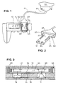
- Figure 1 shows a caliper in partial section with a device according to the subject of the invention.
- FIG. 2 represents a connector used in the device according to the object of the invention.
- Figure 3 illustrates the device in cross section.
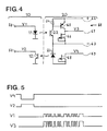
- Figure 4 shows the associated electrical diagram and Figure 5 the related waveforms.
- the instrument 10 here a digital caliper, has a cavity 14, in which the connector 20 is inserted.
- the positioning of this connector 20 is ensured by the shape of the cavity 14, matching that of the connector 20.
- the position of the connector 20 is fixed by the presence of two pins 23 coming in one piece with the body 30 of the connector 20.
- These pins 23 are housed in two recesses 24 provided in the measuring instrument 10 and have a certain elasticity thus controlling the forces of insertion and extraction of the connector 20.
- a polarizing key 25 on the connector 20, as well as a corresponding recess 26 on the measuring instrument guarantee the correct orientation of the connector 20, so that a light-emitting diode 21 and a phototransistor 22 arranged on the connector are well opposite a phototransistor 12 and a light-emitting diode 11 of the measuring instrument (see the section in FIG. 3).
- the connector 20 is extended by a sleeve 27 and a cable 40 connecting the connector 20 to the connector 50 connected to a serial port of an acquisition system 51.
- FIG. 3 shows in section the connector 20 in its cavity 14, where it is arranged opposite the light-emitting diode 11 and the phototransistor 12 mounted on a printed circuit 13 of the caliper 10.
- the arrows indicate the direction of the optical transfer of information: from the light-emitting diode 21 to the phototransistor 12, that is to say from the connector 20 to the caliper 10, and from the light-emitting diode 11 to the phototransistor 22, that is to say from the caliper 10 to the connector 20.
- the connector 20 is made so as to have a small footprint, especially in thickness.
- the body 30 of the connector 20 has a recess 33. On this body are fixed on one side a printed circuit to a layer 31, on which are soldered the light-emitting diode 21, the phototransistor 22, and the other components necessary for obtaining desired signals placed in the rest of the recess 33.
- a transparent cover 32 at least opposite the optoelectric components, closes the connector on the side opposite to the printed circuit.
- the components are preferably of the CMS type (surface-mounted components) in order to reduce the bulk.
- the electronic circuit shown in FIG. 4 is constituted in such a way that the light-emitting diode 11, serving as the photoemitter of the instrument, is inactive, so that the signal V1 generated at the output 53 of a microcontroller of the measuring instrument 10 is zero, when there is no transmission of results.
- the phototransistor 22 serving as a photodetector, is associated with an amplifier circuit 61 comprising two supply lines 62, 63 between which are connected in parallel, on the one hand a resistor 64 (50 KOhm) followed by the phototransistor 22 and, on the other hand, a PNP type transistor 65, the collector of which is connected to a current regulating diode 66 ensuring a constant current (1.5 mA) from a certain potential difference (2 volt ).
- This diode 66 could be replaced by a resistor (3 to 5 KOhm).
- the base of the PNP transistor 65 is connected to the input of the phototransistor 22 and the collector of this PNP transistor 65 supplies via the transmission line 67 the amplified signal V3 to the acquisition unit 51.
- the light-emitting diode 21 of the connector is connected via a second current-regulating diode 68 to the line 69 by which it receives the control signals V4 from the acquisition unit 51, the other terminal of the light-emitting diode 21 being connected to line 63.
- the light emitted by the light-emitting diode 21 is picked up by the phototransistor 12 of the measuring instrument 10 which transmits an electrical signal V2 to the input 52 of the microcontroller.
- line 69 is set to a positive voltage and the light-emitting diode 21 emits a photonic signal of a visible or infrared wavelength, which is picked up and transmitted to the microcontroller.
- the latter can be programmed to recognize the presence of connector 20 by the presence of the photonic signal.
- the control unit 51 requests a measurement result by setting the line 69 to a negative potential, the current in the regulating diode 68 and in the light-emitting diode 21 is stopped.
- the phototransistor 12 then ceases to be conductive and the change in the voltage of the signal V2 can be read by the input 52 of the microcontroller which controls the transmission of a measurement result as described above.
- line 69 can also transmit more specific data from the acquisition unit 51 to the measuring instrument 10, for example preset values or tolerance limits, etc.
- connection and connection device described above is in no way limiting and that it can receive any desirable modifications within the framework defined by the independent claim.
- a connection device operating in both directions, it is possible, according to a simplified variant, only to use a connection comprising only a photoemitter on the side of the instrument and a photodetector disposed on the connector. Instead of being of a generally rectangular shape, the latter may have a completely different geometry.
Landscapes
- Physics & Mathematics (AREA)
- General Physics & Mathematics (AREA)
- Optics & Photonics (AREA)
- Arrangements For Transmission Of Measured Signals (AREA)
- Length Measuring Devices By Optical Means (AREA)
- Optical Transform (AREA)
Applications Claiming Priority (2)
| Application Number | Priority Date | Filing Date | Title |
|---|---|---|---|
| CH3668/89A CH681390A5 (enExample) | 1989-10-06 | 1989-10-06 | |
| CH3668/89 | 1989-10-06 |
Publications (2)
| Publication Number | Publication Date |
|---|---|
| EP0421939A1 EP0421939A1 (fr) | 1991-04-10 |
| EP0421939B1 true EP0421939B1 (fr) | 1995-04-12 |
Family
ID=4260943
Family Applications (1)
| Application Number | Title | Priority Date | Filing Date |
|---|---|---|---|
| EP90810757A Expired - Lifetime EP0421939B1 (fr) | 1989-10-06 | 1990-10-04 | Dispositif de liaison et de connexion pour instruments de mesure |
Country Status (3)
| Country | Link |
|---|---|
| EP (1) | EP0421939B1 (enExample) |
| CH (1) | CH681390A5 (enExample) |
| DE (1) | DE69018564T2 (enExample) |
Family Cites Families (4)
| Publication number | Priority date | Publication date | Assignee | Title |
|---|---|---|---|---|
| US3867567A (en) * | 1973-10-11 | 1975-02-18 | Gte Automatic Electric Lab Inc | Electronic data terminal interface |
| DE3013705C2 (de) * | 1980-04-10 | 1985-10-10 | Siemens AG, 1000 Berlin und 8000 München | Anordnung zur Übertragung von Daten zwischen einem mobilen Datenerfassungsgerät und einem Datenverarbeitungsgerät |
| DE3605627A1 (de) * | 1986-02-21 | 1987-08-27 | Elektron Bremen | Verfahren und vorrichtung zur uebertragung der daten einer spannungsquelle (batterie) auf eine datenverarbeitungsanlage |
| JPS63168600U (enExample) * | 1987-04-16 | 1988-11-02 |
-
1989
- 1989-10-06 CH CH3668/89A patent/CH681390A5/fr not_active IP Right Cessation
-
1990
- 1990-10-04 EP EP90810757A patent/EP0421939B1/fr not_active Expired - Lifetime
- 1990-10-04 DE DE69018564T patent/DE69018564T2/de not_active Expired - Fee Related
Also Published As
| Publication number | Publication date |
|---|---|
| DE69018564T2 (de) | 1995-10-12 |
| CH681390A5 (enExample) | 1993-03-15 |
| DE69018564D1 (de) | 1995-05-18 |
| EP0421939A1 (fr) | 1991-04-10 |
Similar Documents
| Publication | Publication Date | Title |
|---|---|---|
| EP0334254B1 (en) | Magnetically activating optical data link | |
| US6715675B1 (en) | Electronic shelf label systems and methods | |
| CA2036959A1 (en) | Optoelectronic assembly | |
| US20100046955A1 (en) | Integrated transceiver with lightpipe coupler | |
| US8682172B2 (en) | Optoelectronic communications assembly having an electrical and optical interface | |
| CN104272156B (zh) | 将芯片组光学连接到光学连接器的装置、系统及方法 | |
| EP1962173B1 (fr) | Module optoélectronique muni d'au moins un circuit photorécepteur | |
| US20150241645A1 (en) | Methods and apparatus for high speed short distance optical communications using micro light emitting diodes | |
| EP0267085A1 (fr) | Dispositif électronique destiné à permettre l'utilisation d'une carte à mémoire avec un système auquel elle est destinée | |
| EP0940655B1 (fr) | Sonde de mesure comportant au moins une fibre optique, dispositif de mesure et installation comportant au moins une telle sonde | |
| WO2003062891A1 (en) | Passive self-alignment technique for array laser transmitters andreceivers for fiber optic applications | |
| EP0421939B1 (fr) | Dispositif de liaison et de connexion pour instruments de mesure | |
| EP1519457B1 (fr) | Adaptateur pour instrument électronique portable et système de transmission entre ces deux éléments | |
| US7492982B2 (en) | Optical module | |
| FR2816066A1 (fr) | Module de connexion electro-optique | |
| JP2004165299A (ja) | 光送信モジュール及び光送信器 | |
| US6771846B2 (en) | Optical interconnect for mezzanine circuit boards | |
| EP0085633B1 (fr) | Réseau de commutation opto-éléctronique | |
| EP0732023A1 (fr) | Dispositif de commutation pour un poste telephonique a combine permettant la commutation d'un appareil annexe par substitution | |
| CA2035530A1 (en) | Optical signal connection device for units to be inserted in a rack | |
| CN208477157U (zh) | Hdmi连接器装置 | |
| EP1033673B1 (fr) | Dispositif d'aide à l'identification de sous-ensembles d'un équipement, notamment d'aéronef | |
| JP2005301005A (ja) | 光ファイバモジュール | |
| FR2691264A1 (fr) | Système de raccordement de liaisons optiques à des liaisons électriques. | |
| RU181218U1 (ru) | Модуль фотоприёмный высокочастотный |
Legal Events
| Date | Code | Title | Description |
|---|---|---|---|
| PUAI | Public reference made under article 153(3) epc to a published international application that has entered the european phase |
Free format text: ORIGINAL CODE: 0009012 |
|
| AK | Designated contracting states |
Kind code of ref document: A1 Designated state(s): DE FR GB |
|
| 17P | Request for examination filed |
Effective date: 19910715 |
|
| 17Q | First examination report despatched |
Effective date: 19940510 |
|
| GRAA | (expected) grant |
Free format text: ORIGINAL CODE: 0009210 |
|
| AK | Designated contracting states |
Kind code of ref document: B1 Designated state(s): DE FR GB |
|
| REF | Corresponds to: |
Ref document number: 69018564 Country of ref document: DE Date of ref document: 19950518 |
|
| GBT | Gb: translation of ep patent filed (gb section 77(6)(a)/1977) |
Effective date: 19950518 |
|
| PLBE | No opposition filed within time limit |
Free format text: ORIGINAL CODE: 0009261 |
|
| STAA | Information on the status of an ep patent application or granted ep patent |
Free format text: STATUS: NO OPPOSITION FILED WITHIN TIME LIMIT |
|
| 26N | No opposition filed | ||
| PGFP | Annual fee paid to national office [announced via postgrant information from national office to epo] |
Ref country code: GB Payment date: 20000922 Year of fee payment: 11 |
|
| PGFP | Annual fee paid to national office [announced via postgrant information from national office to epo] |
Ref country code: FR Payment date: 20001002 Year of fee payment: 11 |
|
| PG25 | Lapsed in a contracting state [announced via postgrant information from national office to epo] |
Ref country code: GB Free format text: LAPSE BECAUSE OF NON-PAYMENT OF DUE FEES Effective date: 20011004 |
|
| REG | Reference to a national code |
Ref country code: GB Ref legal event code: IF02 |
|
| GBPC | Gb: european patent ceased through non-payment of renewal fee |
Effective date: 20011004 |
|
| PG25 | Lapsed in a contracting state [announced via postgrant information from national office to epo] |
Ref country code: FR Free format text: LAPSE BECAUSE OF NON-PAYMENT OF DUE FEES Effective date: 20020628 |
|
| REG | Reference to a national code |
Ref country code: FR Ref legal event code: ST |
|
| PGFP | Annual fee paid to national office [announced via postgrant information from national office to epo] |
Ref country code: DE Payment date: 20071025 Year of fee payment: 18 |
|
| PG25 | Lapsed in a contracting state [announced via postgrant information from national office to epo] |
Ref country code: DE Free format text: LAPSE BECAUSE OF NON-PAYMENT OF DUE FEES Effective date: 20090501 |