EP0421639A2 - Système de traitement de données en parallèle - Google Patents
Système de traitement de données en parallèle Download PDFInfo
- Publication number
- EP0421639A2 EP0421639A2 EP90310302A EP90310302A EP0421639A2 EP 0421639 A2 EP0421639 A2 EP 0421639A2 EP 90310302 A EP90310302 A EP 90310302A EP 90310302 A EP90310302 A EP 90310302A EP 0421639 A2 EP0421639 A2 EP 0421639A2
- Authority
- EP
- European Patent Office
- Prior art keywords
- data processing
- matrix
- data
- vector
- tray
- Prior art date
- Legal status (The legal status is an assumption and is not a legal conclusion. Google has not performed a legal analysis and makes no representation as to the accuracy of the status listed.)
- Granted
Links
Images


Classifications
-
- G—PHYSICS
- G06—COMPUTING; CALCULATING OR COUNTING
- G06N—COMPUTING ARRANGEMENTS BASED ON SPECIFIC COMPUTATIONAL MODELS
- G06N3/00—Computing arrangements based on biological models
- G06N3/02—Neural networks
- G06N3/10—Interfaces, programming languages or software development kits, e.g. for simulating neural networks
-
- G—PHYSICS
- G06—COMPUTING; CALCULATING OR COUNTING
- G06F—ELECTRIC DIGITAL DATA PROCESSING
- G06F15/00—Digital computers in general; Data processing equipment in general
- G06F15/16—Combinations of two or more digital computers each having at least an arithmetic unit, a program unit and a register, e.g. for a simultaneous processing of several programs
- G06F15/163—Interprocessor communication
- G06F15/173—Interprocessor communication using an interconnection network, e.g. matrix, shuffle, pyramid, star, snowflake
- G06F15/17337—Direct connection machines, e.g. completely connected computers, point to point communication networks
-
- G—PHYSICS
- G06—COMPUTING; CALCULATING OR COUNTING
- G06F—ELECTRIC DIGITAL DATA PROCESSING
- G06F15/00—Digital computers in general; Data processing equipment in general
- G06F15/76—Architectures of general purpose stored program computers
- G06F15/80—Architectures of general purpose stored program computers comprising an array of processing units with common control, e.g. single instruction multiple data processors
- G06F15/8007—Architectures of general purpose stored program computers comprising an array of processing units with common control, e.g. single instruction multiple data processors single instruction multiple data [SIMD] multiprocessors
- G06F15/8015—One dimensional arrays, e.g. rings, linear arrays, buses
Definitions
- the present invention relates to a parallel data processing system and, more particularly, to a parallel data processing system for processing data using a plurality of data processing units synchronously.
- the number effect means that an improvement in data processing speed which is proportional to the number of processing units used is obtained.
- it is very important to obtain a good number effect.
- the main cause of the deterioration of the number effect is prolongation of the total processing time due to addition of data transfer time to inherent data processing time. To improve the number effect, therefore, it is effective to fully utilize the capacity of data transmission lines. However, it is very difficult.
- the parallel processing system utilizing the regularity of processing is a systolic array system.
- a one-dimensional systolic array system called a ring systolic array system is a parallel data processing system which processes systolic data using a plurality of data processing units synchronously and is easy to implement.
- the processing with regularity includes parallel processing which applies a nonlinear function to a matrix operation based on the inner product of vectors and a sum-of-products operation in a neural network.
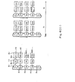
- FIG. 1A illustrates the principle structure of a conventional common-bus-coupled parallel processing system.
- PE designates a processor element
- M designates a memory
- COMMON BUS designates a common bus
- BUS1 designates a bus coupled to the common bus
- BUS2 designates an internal bus for coupling each of the processor elements PE to its corresponding respective memory M.
- communications among the processor elements hereinafter referred to as PEs
- the communications must be performed synchronously over the entire common bus.
- Figure 1 B is an operational flowchart of calculation of the product of a matrix and a vector by the common-bus-coupled parallel system.
- Each PE multiplies Y in its internal register by data X from another PE and adds the resultant product to Y. For this reason, as illustrated in the flowchart, the contents, i.e., Y of the internal register of the i-th PE is first cleared to 0. Then, the following step is repeated n times. That is, when X j is applied to the common bus, the i-th PE multiplies an input from the bus BUS1 connected to the common bus and an input supplied from the memory M through the internal bus BUS2 and adds the resultant product to Y i . This operation is repeated.
- FIG. 2A illustrates the principle of a conventional ring systolic system.
- a processor element PE is connected to another PE by a cyclic common bus.
- M designates a memory for storing coefficients W ij .
- W11, Wi 2 , ..W 33 are elements of a coefficient matrix.
- W ij is an element at the intersection of the i-th row and the j-th column of the matrix.
- the multiplication of the coefficient matrix W and a vector is made by the ring systolic system as follows.
- FIG. 2B illustrates the internal structure of the i-th processor element.
- MULTIPLIER designates a multiplier
- ADDER designates an adder
- ACC designates an accumulator
- M designates a group of registers for storing coefficient elements W ij .
- Each of the registers is of a FIFO (fast-in fast-out) type.
- the element W ij at the intersection of the i-th row and the j-th column of the coefficient matrix is now being read out of the register.
- the element read out of the register is circulated in sync with the next clock to enter the last stage via a bus BUS1.
- W i1 , ..., W j1- have already been circulated and stored in the last stages.
- each element of the vector is entered via the bus BUS1.
- an element X j is entered.
- the result of the inner product of W i1 x X 1 + ... + W j-1 x X j-1 has already been stored in the accumulator ACC.
- This is now output from the accumulator 25 and entered into the adder via its input.
- X j entered from the outside and W ij output from the FIFO register are multiplied in the multiplier.
- the result of the multiplication is input to the adder via its other input so that it is added to the current contents of the accumulator ACC.
- the output of the adder is applied to the same accumulator ACC in sync with the next clock.
- the switch SWITCH is adapted to cause data X i to pass through the processor element PE or set data X into the accumulator ACC.
- PE-1 When the product of a matrix and a vector is calculated in such a PE, PE-1 first multiplies W 11 and X 1 as shown in Figure 2A. During the next clock cycle X 2 flows out of the right PE-2 and W 12 is output from the memory M-1 so that W 12 X 2 is calculated. Similarly, the product of W 13 and X 3 is obtained during the next clock cycle. Thereby, the product of the first column of the coefficient matrix and the vector becomes possible to implement in the PE-1. Also, the product of the second column and the vector is calculated in PE-2. That is, W 22 and X 2 are multiplied, W 23 and X 3 are multiplied during the next clock cycle, and the product of W 21 and cyclically returned X 1 is obtained during the next clock cycle.
- the product of the third row and the vector can be obtained by multiplying W 33 and X 3 , multiplying W 31 and circulating X 1 , and multiplying W 32 and cyclically returned X 2 .
- the product of W 11 and X 1 , the product of W 22 and X 2 , and the product of W 33 and X 3 can be obtained simultaneously.
- torsion is produced in the arrangement of elements of the coefficient matrix in order to carry out the simultaneity.
- Figure 2C illustrates a multi-stage arrangement of the ring systolic configuration of Figure 2A which permits the product of a continuous matrix and a vector.
- Such a systolic array system is regular in processing, thus permitting the capacity of data transmission lines to be fully utilized and thus the number effect to be improved.
- the number effect can be achieved by carrying out the data transfer between PEs and data processing in each PE synchronously.
- the data transfer between PEs and the data processing in each PE must be timed.
- PEs which are not involved in actual data processing are needed, that is, idle PEs increase in number, thus deteriorating the number effect.
- SIMD Single Instruction Multi Data
- a feature of the present invention resides in a parallel data processing system comprising a plurality of data processing units each having at least one input, a plurality of trays each having a first input and an output and functions of storing and transferring data, each of all or part of the trays having a second output connected to the first input of a respective one of the data processing units, and the trays being connected in cascade to form a-shift means and means for performing data transfer through the shift means, data transfer between corresponding ones of the trays and the data processing units and data processing in the data processing units synchronously, thereby performing a matrix operation or a neuron-computer operation on analog signals.
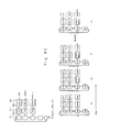
- Figure 3A illustrates the principle of the present invention.
- 1 1 , 1 2 ,... designates a data processing unit
- 2i, 2 2 ... designates a tray for storing and transferring data
- 3 designates a shift register constructed by interconnecting the trays
- 11 designates a first input of the data processing unit
- 12 designates a second input of the data processing unit
- 21 designates a first input of the tray
- 22 designates a first output of the tray
- 23 designates a second output of the tray 2.
- the data processing units 1 process data.
- the trays 2 transfer data and form a shift register 3 for shifting data cyclically.
- the present invention allows the product of a m x n matrix A and a vector with n elements to be calculated by the use of m data processing units and n trays in a processing time proportional to n even if the number m of rows of the matrix /A is smaller than the number n of columns or m is larger than n, thereby achieving a good number effect.
- each of the data processing units 1 multiplies an input from 11 and an input from 12, adds the product to the contents of its accumulating register Y and then shifts an element of the vector between adjoining trays in the shift register 3.
- the present invention unlike the conventional system, can achieve a good number effect without the need for any timing process by separating the data processing units 1 and the trays 2 having data storage function even if m and n differ from each other. Furthermore, the present invention can make the data transfer time negligible as compared with data processing time because the data transfer between trays 2 and data processing by data processing units 1 are performed concurrently and, in general, the data transfer time can be expected to be shorter than the data processing time required by the data processing units. Therefore, the data transfer time can be hidden by the data process time.
- Figure 3B is an operational flowchart of a basic configuration of the present invention illustrated in Figure 3A.
- data processing units 1 and trays 2 having data storage function are separated.
- the adjacent trays 2 are connected in a ring to form a systolic system.
- n corresponds to the number of the data processing units and n corresponds to the number of the trays.
- X i is set in the i-th tray 2.
- the value of Y i in an accumulating register of data processing unit i is set to 0. That is, the contents of the accumulating register of the i -th data processing unit are initialized.
- the i-th processing unit 1 i multiplies an input from 11 i and an input from 12 i and then adds the resultant product to the contents of the accumulator Y i , thereby performing a partial minor product operation.
- the i-th processing unit 1 then shifts the contents of the shift register 3.
- the calculation of the inner product and the shift operation are repeated n times.
- the product of the rectangular matrix /A and the vector is formed. In this case, data transfer between trays and data processing in data processing units are performed concurrently.
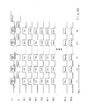
- Figure 3C is a conceptual diagram of the operation of the system of the present invention.
- data X 1 to X n in the trays 2 are elements of the vector and the number of the elements is n.
- the data processing units are m in number and incorporate their respective accumulators Y1, Y2,.., Ym.
- the m x n rectangular matrix have elements from A" to A mn and hence m x n elements.
- a 11 , A 12 , ...A 1n in the first row of the coefficient matrix are entered in sequence at respective timing steps in the systolic operation into the data processing unit 1 1 from the input bus 12 1 .
- the data processing unit 1 2 is supplied with A 22 , A 23 ,...A 21 in sequence at respective timing steps in the systolic operation.
- the data processing unit 1 m is supplied with A mm , A m m+1 ,..., A m m-1 in sequence at respective timing steps in the systolic operation.
- Figure 3D is a timing chart of the operation illustrated in Figure 3C.
- the operations at Ti, T 2 , T 3 and T n in Figure 3C correspond to those at Ti, T 2 , T 3 and T n in Figure 3D.
- data Xi, X 2 , ..X m ,..X n are present in the trays 2 1 , 2 2 ,...2 n , respectively, and A 11 , A 22 , ...A mm , which are the elements of the coefficient matrix, are present in the data processing units 1 1 , 1 2 ,...1 m .
- data process unit 1 1 obtains a product of A 11 and data X 1 in tray 2 1
- data processing unit 1 2 obtains a product of A 22 and data X 2
- data processing unit 1 m obtains a product of A mm and data X m . That is, at a sync clock for obtaining the sum of products, X 1 is present at the bus 11 1 , A 11 at the bus 12 1 , X 2 at bus 11 2 , A 22 at 12 2 , X 3 at 11 3 , A 33 at 12 3 , X m at 11 m and A mm at 12 m .
- the inner product is calculated at time T i .
- a 12 , A 23 , ..., A m m+i which are the elements of the coefficient matrix, are entered into the trays 1, 2, ..., m, respectively.
- Data present on the buses at time T 2 are illustrated in Figure 3D.
- the product of A 1 and X 2 is obtained and then added to the contents of the accumulator Y.
- the product of A 11 and X 1 obtained at time T, and the product of A 12 and X 2 obtained at time T 2 are summed and the result is stored in the accumulator.
- a 22 x X 2 + A 23 x X 3 is stored in the accumulator. This is the case with the unit 1m.
- Figure 4A is a detailed block diagram of the configuration of Figure 3 for calculating the product Y (m elements) of a m x n (n ⁇ m > 1) matrix /A and a vector with n elements.
- like reference characters are used to designate corresponding parts to those in Figure 3A.
- 1 a designates a processor of the data processing unit 1, which may be constructed from a digital signal processor
- 2a designates a data storage circuit of the tray 2, which may be constructed from a latch circuit
- 2b designates a data transfer circuit of the tray 2, which may be constructed from a bus driver
- 2c designates control means of the tray 2, which may be constructed from logic circuits
- 4 designates a memory device which forms a part of means for supplying data to the data processing unit 1 and a part of means for controlling the data processing unit 1 and may be constructed from a RAM (random access memory)
- 5 designates means for establishing synchronization between the data processing units 1 and the trays 2.
- 5a designates a clock generator which may be constructed from a crystal oscillator
- 5b designates a clock distributor which may be constructed from a buffer circuit.
- Figure 4B is a flowchart of the system of the present invention illustrated in Figure 4A.
- the data processing units 1 and the trays 2 having a function of storing data are separated from each other, and the trays 2 are connected in a ring to form a systolic system.
- the product of a m x n matrix /A and a vector with n elements is calculated in accordance with a flowchart of Figure 6B.
- X i is set in tray 2 i .
- the contents of Y i is set to 0. Whereby, the contents of the accumulating register in the i-th data processing unit is initialized.
- the i-th processing unit 1 i multiplies an input from 11 i and an input from 12 i and then adds the resultant product to the contents of the accumulator Y i . Then, the contents of the shift register 3 are shifted. The inner product calculation and the shift operation are repeated n times. As a result of this processing, the product of the rectangular matrix /A and the vector is formed. In this case, data transfer between trays and data processing in each data processing unit are performed concurrently.
- Figure 4C is a conceptual diagram of the operation of the system of the present invention and shows a systolic operation performed in the same manner as in Figure 3C.
- data X 1 to X n in the tray 2 which are elements of the vector , be n in number.
- m x n elements of A 11 to A mn are present in an m x n rectangular matrix.
- a 11 , A 12 .., A 1n which are the elements in the first row of the coefficient matrix, are synchronously entered into the data processing unit 1 1 from an input bus 12 1 .
- a 22 , A 23 , .., A 21 are entered into the data processing unit 1 2 in the sequence of timing steps of the systolic operation.
- a mm , A m m+1 ,..., A m m - 1 are synchronously entered into the data processing unit 1 m .
- Figure 4D is a timing chart of the operation illustrated in Figure 4C.
- Time intervals T 1 to T n , in Figure 4C correspond to times Ti, T 2 ,.., T n of Figure 4D.
- X 1 , X 2 , X m ,.., X n are present in the trays 2 1 , 2 2 , ..., 2 n , respectively, as illustrated in Figure 4C.
- Into the data processing units 1 1 , 1 2 , ..., 1 m are respectively entered A 11 , A 22 , ..., A mm which are elements of the coefficient matrix.
- X 1 is present on the bus 11 1
- a 11 is present on the bus 12 1
- X 2 is present on the bus 11 2
- a 22 is present on the bus 12 2
- X 3 is present on the bus 11 3
- a 33 is present on the bus 12 3
- X m is present on the bus 11 m
- a mm is present on the bus 12 m .
- the calculation of the inner product is performed at time T1 as illustrated in Figure 4C.
- the value of the accumulator Y is 0 at this point.
- the result is the sum of the inner product and 0.
- the shift operation is performed between T 1 and T 2 , during which time data is shifted between adjoining trays. That is, the left shift is performed in this case. Then, the operation advances to time T 2 in Figure 4C and the operation timing also advances to time T 2 in Figure 4D, thereby performing an operation of the time of the products.
- X 2 is stored in the tray 2 1
- X 3 is stored in the tray 2 2
- X m+1 is stored in the tray 2 m .
- Into the trays 2 1 , 2 2 ,.., 2 m are entered A 12 A23, A m m+1 , respectively. Data present on the buses are indicated on time slot T 2 of Figure 4D.
- the product of A 12 and X 2 is formed at T 2 and added to the previous contents of the accumulator Y.
- the product of A 11 and X 1 obtained at T 1 and the product of A 12 and X 2 obtained at T 2 is summed and the result is stored in the accumulator.
- a 22 x X 2 + A 23 x X 3 is stored in the accumulator in the unit 1 2 . This is the case with the unit 1 m .
- the shift operation is performed again and then time T 3 arrives.
- X 3 is shifted to the tray 2 1
- X 4 . is shifted to the tray 2 2
- X m+2 is shifted to the tray 2 m
- X 2 is shifted to the tray 2 n .
- the calculation of inner product is carried out at time T 3 as illustrated in Figure 4C.
- a 1n x X n is added to the sum of the products, i.e., the sum of A 11 x X 1 obtained at Ti, A 12 X 2 obtained at T 2 , A 13 x X 3 obtained at T 3 ,..., and A 1 n-1 x X n - 1 obtained at T n-1 , the sum having been stored in the accumulator Y in the tray 2 1 , so that the inner product of the first row of the matrix /A and the vector is calculated.
- the calculation of the inner product of the second row of the matrix /A and the vector is performed in n clock cycles.
- the inner product of the m-th row of the matrix and the vector is calculated by the data processing unit 1 m .
- Figure5A illustrates a second embodiment of the present invention. More specifically, Figure 5 illustrates a configuration of a systolic system for multiplying the product of a m x n matrix /A and a vector with n elements by a k x m matrix
- 1a designates a processor of the data processing unit 1, which may be constructed from a digital signal processor.
- 2a designates a data storage circuit of the tray 2, which may be constructed from a latch circuit
- 2b designates a data transfer circuit of the tray 2, which may be constructed from a bus driver
- 2c designates control means of the tray 2, which may be constructed from logic circuits.
- 4 designates a memory device which forms a part of means for supplying data to the data processing unit 1 and a part of means for controlling the data processing unit 1 and may be constructed from a RAM (random access memory).
- 5 designates means for establishing synchronization between the data processing units 1 and the trays 2.
- 5a designates a clock generator which may be constructed from a crystal oscillator, and
- 5b designates a clock distributor which may be constructed from a buffer circuit.
- 6 designates a selector for selecting among data returned systolically, data input to the tray and external data
- 7 designates selectors for bypassing systolic data halfway.
- the present embodiment is exactly the same as the first embodiment in operation as far as the intermediate result /Ax is obtained.
- the elements of the intermediate result /Ax are stored in the respective data processing units, (a) the elements of the intermediate result are written into the corresponding trays 2, (b) the bypassing selector 7 is turned on to alter the length of the shift register to m, and (c) the matrix / A is changed to the matrix
- Figure 5B is an operational flowchart of the second embodiment
- Figure 5C is a schematic diagram illustrating the operation of the second embodiment
- Figure 5D is a timing chart of the operation of the second embodiment.
- B from the left is performed in accordance with the flowchart of Figure 5B.
- X i is set in the tray 2 i .
- the value of Y is set to 0. That is, the value of the accumulating register in the i-th data processing unit is initialized.
- the i -th processing unit 1 i multiplies an input from 11 i and an input from 12 i and then adds the resultant product to the contents of the accumulator Y i .
- the shift register 3 is shifted.
- the calculation of the inner product and the shift operation are repeated n times. As a result of this process, the product of the rectangular matrix /A and the vector is formed.
- the length of the shift register is changed to m and the contents of Y are transferred to the tray 2 i .
- the i-th processing unit 1 multiplies an input from 11 and an input from 12 i and then adds the resultant product to the contents of an accumulator Z i .
- the contents of the shift register 3 are then shifted.
- the calculation of the inner product and the shift operation are repeated k times.
- Figure 5C is a conceptual diagram of the above operation.
- data X 1 to X n in the trays 2 are elements of the vector whose number is n.
- m data processing units are effective and have accumulators Y 1 , Y 2 ,..., Y m .
- the m x n rectangular matrix /A has m x n elements of A 11 to A mn .
- a 11 , A 12 ,..., A 1n which are elements in the first row of the coefficient matrix, are synchronously entered into the data processing unit 1 1 from the input bus 12 1 .
- the data processing unit 1 2 is supplied with A 22 , A 23 , ..., A 21 in the sequence of timing steps of the systolic operation.
- the data processing unit 1 m is supplied with A mm , A m m+1 ,.., A m m-1 synchronously.
- Figure 5D is a timing chart of the operation illustrated in Figure 5C. In respect of operations during time intervals T 1 to T n , Figure 5C correspond to Figure 5D.
- elements Xi, X 2 ,.., X k ,.., X n of vector x are present in the trays 1, 2, .., n, respectively, as illustrated in Figure 5C.
- In the data processing units 1, 2,.., k, ..., m are respectively stored A 11 , A 22 ,..,A kk ..., A mm which are elements of the coefficient matrix.
- element X 1 of vector is present on the bus 11 1
- element A 11 of coefficient matrix /A is present on the bus 12 1
- X 2 is present on the bus 11 2
- a 22 is present on the bus 12 2
- X k is present on the bus 11 k
- a kk is present on the bus 12 k
- X m is present on the bus 11 m
- a mm is present on the bus 12 m .
- the calculation of the inner product is performed at time T 1 as illustrated in Figure 5C.
- the value of the accumulator Y is 0 at this point.
- the result is the sum of the inner product and 0.
- the shift operation is performed between T 1 and T 2 , during which time data is shifted between adjoining trays. That is, the left shift is performed in this case. Then, time T 2 arrives in Figure 5C. Likewise, time T 2 arrives in Figure 5D, thereby performing an operation of the sum of the products.
- X 2 is stored in the tray 1
- X 3 is stored in the tray 2
- X k+1 is stored in the tray k
- X m+1 is stored in the tray m.
- a 22 x X 2 + A 23 x X 3 is stored in the accumulator in the tray 2. This is the case with the trays k and m.
- the shift operation is performed again and time T 3 ; arrives.
- X 3 is shifted to the tray 1
- X 4 is shifted to the tray 2
- X k+2 is shifted to the tray k
- X m m+2 is shifted to the tray m
- X 2 is shifted to the tray n.
- the calculation of inner products is carried out at time T 3 as illustrated in Figure 5C.
- Aim x X m will, as shown in time T m in Figure 5D, be added to the sum of the so-far-obtained products, i.e., the sum of A 11 x X 1 obtained at Ti, A 12 x X2 ) obtained at T 2 , A 13 x X3 obtained at T 3 ,..., and A 1 k x X k obtained at T k , which has been stored in the accumulator Y in the tray 1, so that the inner product of the first row of the matrix /A and the vector is calculated.
- the calculation of the inner product of the second row of the matrix /A and the vector is performed in n clock cycles.
- the inner product of the k-th row of the matrix and the vector is calculated by the data processing unit 1 k .
- B and a vector with m elements is performed.
- An i-th element is set in the tray 2 i .
- the value of Z i is set to 0. That is, the value of the accumulating register of the i-th data processing unit is initialized.
- the i-th processing unit 1 i multiplies an input from 11 i and an input from 12 i and then adds the resultant product to the contents of the accumulator Z i .
- the contents of the shift register 3 are then shifted. This calculation of the inner product and shift operation are repeated m times, corresponding to dimension As a result of this process, the product of the rectangular matrix
- Figure 5D is a timing chart of the operation illustrated in Figure 5C.
- Figure 5C corresponds to Figure 5D.
- Y 1 , Y 2 ,.., Y m are present in the trays 1, 2, .., m, respectively, as illustrated in Figure 5C.
- B 11 , B 22 , ..., B kk which are elements of the coefficient matrix
- the shift operation is performed between T n+2 and T n+3 , during which time data is shifted between adjoining trays. That is, the left shift is performed in this case.
- time T n+3 arrives in Figure 5C.
- Time T n+3 arrives in Figure 5D, thereby performing an operation of the sum of the products.
- Y 2 is stored in the tray 1
- Y 3 is stored in the tray 2
- Y k+1 is stored in the tray k.
- k are entered elements B 12 , B 23 , B k k+1 of coefficient matrix
- Data present on the buses are indicated on time slot T n+3 of Figure 5D.
- the product of B 12 and Y 2 is formed at T n+3 and then added to the previous contents of the accumulator Z.
- the sum of the product of B 11 and Y 1 obtained at T n+2 and the product of B 12 and Y 2 obtained at T n+3 is obtained and the result is stored in the accumulator Z.
- B 22 x Y 2 + B 23 x Y 3 is stored in the accumulator Z in the unit 2. This is the case with the tray k.
- the shift operation is performed again and then time T n+4 arrives.
- B 1m x Y m is added to the sum of the so-far- stored products, i.e., the sum of B 11 x Y 1 obtained at T n+2 , B 12 x Y2 obtained at T n+3 , B 13 X Y3 obtained at T n+4 , and so on, the sum having been stored in the accumulator Z in the unit 1, so that is added to the sum of the inner products stored in the accumulator Z at time T n+m+1 and the inner product of the first row of the matrix [B and the vector is calculated.
- the unit 2 the calculation of the inner product of the second row of the matrix B and the vector is performed.
- the inner product of the k-th row of the matrix B and the vector is calculated by the data processing unit 1 k .
- the length of the shift register 3 can be changed, and the intermediate result can be written into the trays 2 and processed as new data. If the length of the shift register 3 could not be changed, n unit times would be needed to circulate all the data.
- the capability of processing of intermediate results as new data will permit the execution of a wider range of processes with small-scale hardware than in the ring systolic array system.
- it is important that a time required to write data into the shift register is short and constant.
- Figure 6A illustrates a third embodiment of the present invention.
- This system is configured to calculate the product of the transposed matrix /AT of an m x n rectangular matrix /A, i.e., a (n x m) matrix, and a vector with m elements.
- a (n x m) matrix i.e., a (n x m) matrix
- m elements i.e., a (n x m) matrix
- row vectors constituting the matrix /A are each stored in respective memories 4 coupled to data processing units 1 and data are circulated through the shift register 3 while a partial sum of products obtained in the middle of calculating are accumulated in data storage circuits 2a in the trays.
- FIG. 6A is a detailed block diagram of the third embodiment in which the product (n elements) of an n x m (n ⁇ m ⁇ 1) matrix /AT and a vector with m elements is calculated.
- 1a designates a processor of the data processing unit 1, which may be constructed from a digital signal processor.
- 2a designates a data storage circuit of the tray 2, which may be constructed from a latch circuit
- 2b designates a data transfer circuit of the tray 2, which may be constructed from a bus driver
- 2c designates control means of the tray 2, which may be constructed from logic circuits.
- 5 designates means for establishing synchronization between the data processing units 1 and the trays 2.
- 5a designates a clock generator which may be constructed from a crystal oscillator
- 5b designates a clock distributor which may be constructed from a buffer circuit.
- Figure 6B is an operational flowchart of the third embodiment.
- the multiplication of a transposed matrix and a vector is made possible with each of the row vectors of the matrix /A stored in a memory 4 without changing an arrangement of data, i.e., without transposing the matrix /A.
- the amount of calculation in the network is of the order of m.
- the data transfer time is negligible as compared with the processing time so that there is no overhead for the transfer time. Further, this operation is applied to a SIMD method.
- FIG. 6C is a schematic diagram illustrating the operation of the third embodiment.
- a 11 to Aim are entered into the unit 1 1 in sequence.
- a 22 , A 23 ,..A 21 are entered into the unit 1 2
- a kk , A k k+1 ,..., A k k-1 are entered into the k-th unit through a memory circuit starting with a diagonal element A 22 .
- a mm , A m m + 1 ,..., A m m-1 are entered into the m-th unit.
- Y 1 to Y n circulate through the trays.
- FIG. 6D is a timing chart of the operation of the third embodiment.
- Data present on the buses provided between the memory and data processing unit and between the data processing unit and tray are indicated on time slots T 1 to T n and they correspond to those in Figure 6 C.
- Y 1 to Y n are all 0 in time slot T 1 .
- the product of A 1 and X 1 is formed by the unit 1 1 and then added to Y i .
- a 22 and X 2 are added to Y 2
- a kk x X k is added to Y k
- a mm x X m is added to Y m .
- a shift operation is performed and then time T 2 arrives. That is, Y data circulate.
- a 12 x X 1 is calculated and then added to the content of Y 2 which is A 22 x X 2 obtained at Ti.
- Y 2 A 22 x X 2 + A 12 x x X 1 .
- a 23 x X 2 is added to the previous content of Y 3 , thereby providing A 33 x X 3 + A 23 x X2.
- a k k + 1 x X k is added to Y k+1 .
- a m m + 1 x X m is added to Y m + 1 .
- a 1n x X 1 is added to Y n which has been obtained by then in the first unit 1 1 .
- a 21 x X 2 is added to Y 1 in unit 1 2 .
- the first element X 1 of the vector is multiplied by A 11 at T 1 so that A 11 x X 1 is calculated. This is stored in Yi.
- the second element A 21 x X 2 in the first row of the transposed matrix /A T is calculated in the last clock cycle T n . This is stored in the same Y 1 .
- the product of the last element A m1 in the first row of the transposed matrix /A and X m is calculated by the m-th unit in the clock cycle T n-m+2 of Figure 6C. That is, the product of A m1 and X m is obtained by being added to Yi. This is the case with the second row of the transposed matrix /A T .
- the product of A 12 and X 1 is calculated by the unit 1 in the clock cycle T 2 .
- a 22 x X 2 is obtained by the second unit in the clock cycle Ti. It is in the time slot T n-m+3 that Y 2 is recirculated to obtain a product. After the time slot T n-m+3 the multiplication and shift operation are performed.
- Y k - 2 + A k k - 2 x X k is calculated in time slot T 3 .
- Y k - 1 + A k k - 1 x X k is calculated in time slot T n-1 .
- the product of the transposed matrix /A T and m-dimensional vector x is calculated. That is, to calculate the transposed matrix /A T and the vector , partial row vectors constituting the matrix /A are each stored in respective memories 4 connected to the data processing units 1 and the partial sums yielding in the middle of calculation are circulated through the shift register while they are accumulated in the data storage circuits of the trays 2.
- the partial row vectors of the matrix /A stored in the memories 4 connected to the data processing units 1 and used in calculating the product of the matrix /A and the vector u may be used as they are without transferring the partial matrices of the transposed matrix /A T to the data processing units 1. It is not necessary to transpose matrix /A in a memory when the transposed matrix /A is calculateted in the present embodiment. Thus, the transfer time can be saved and the process time can be further shortened.
- Figure 6E is a detailed flowchart of the step to be repeated of Figure 6B.
- each unit 1 adds the product of A ii and X i to Y i and write the result of the sum of the products in tray 3 again. Namely, Then, tray 3 is shifted.
- each unit 1 i adds the product of A i i+1 and X to Y i + 1 and the result of the sum of the products is written in tray 3. Namely, Then tray 3 is shifted.
- each unit 1 i adds the product of A i , i + n-1 and X i to Y i + n-1 and writes the result of the sum of the products in tray 3 again. Namely, Then, the tray 3 is shifted.
- Figure 7A illustrates of a fourth embodiment of the present invention.
- the present embodiment is directed to a neuro-computer.
- like reference characters are used to designate corresponding parts to those in Figure 6.
- 1a designates a processor of the data processing unit 1, which may be constructed from a digital signal processor.
- 2a designates a data storage circuit of the tray 2, which may be constructed from a latch circuit
- 2b designates a data transfer circuit of the tray 2, which may be constructed from a bus driver
- 2c designates control means of the tray 2, which may be constructed from logic circuits.
- 4 designates a storage device which forms a part of means for supplying data to the data processing unit 1 and a part of means for controlling the data processing unit 1 and may be constructed from a RAM (random access memory).
- 5 designates means for establishing synchronization between the data processing units 1 and the trays 2.
- 5a designates a clock generator which may be constructed from a crystal oscillator
- 5b designates a clock distributor which may be constructed from a buffer circuit.
- 101 designates a sigmoid function unit which calculates a monotone nondecreasing continuous function which is referred to as a sigmoid function and its differential coefficient, the function being approximated by a polynominal.
- 103 designates means for deciding the end of learning, which may be constructed from a host computer connected with the data processing units through communication means, means for informing an output error calculated by each processing unit 1 of the host computer and means for deciding the end of learning on the basis of a plurality of values of output errors to bring the neuro-computer to a stop.
- 102 designates the whole of the neuro-computer.
- Figure 7B illustrates a neuron model which is a basic element of the neuro-computer of the present invention.
- the neuron model multiplies inputs Xi, X 2 ,..., X n by weights Wi, W 2 ,..., W n serving as synapses, respectively, and obtains the sum of the products which is used as an internal value U.
- a nonlinear function f is applied to the internal value U to provide an output Y.
- Such an S-shaped sigmoid function as illustrated is generally used herein for the nonlinear function f.
- Figure 7C is a conceptual diagram of a hierarchical neural network constituting a neuro-computer of a three-layer structure comprised of an input layer, an intermediate layer and an output layer using a plurality of neuron models of Figure 7D.
- the input layer which is the first layer, receives input signals I 1 , I 2 ,.., I N(1)
- Each of units, i.e., neuron models, of the second intermediate layer is connected to all the neuron models in the first layer.
- the tie-branches therefor are synapses which are given respective weights W ij .
- the third output layer also has each of its units or neuron models connected to all the neuron models of the intermediate layer. The outputs are drawn to the outside.
- an error between a teacher signal corresponding to input pattern signals applied to the input layer at the time of learning and an output signal from the output layer is obtained.
- the weights between the intermediate layer and the output layer and the weights between the first and second layers are determined so that the error may become very small.
- This algorithm is called the law of back propagation learning.
- an associative process such as pattern recognition
- an output signal corresponding to the pattern is output from the output layer.
- the signal is very similar to a teacher signal corresponding to the pattern applied at the time of learning. If the difference between the output signal and the teacher signal is very small, the imperfect pattern will become recognized.
- the operation of the neural network can be implemented with the neuro-computer 102 of Figure 7A on an engineering basis. Though such a three-layer network as shown in Figure 7C is used in the present embodiment, the number of layers has no essential influence on the operation of the present embodiment as will be described below.
- N(1) stands for the number of neurons of the first layer.
- the output of each neuron of the first layer, or the input layer is equal to its input. Thus, there is no need of substantial processing.
- the forward process in the normal process that is, pattern recognition, is illustrated in Figure 7D.
- FIG 7D is a flowchart of the forward process of the fourth embodiment. It is assumed in the forward process that the weight coefficients on the tie-branches between layers in the network of Figure 7C are determined.
- the basic operation in the forward operation is to, in the neuron model of Figure 7B, multiply inputs by weights and apply a nonlinear function to the sum U of products. This operation is performed for each of the layers.
- step 70 data from 1 1 to I N(1) are set in the shift register. With the number of layers represented by L, the following processes are all repeated for each of the layers. If L is 3, for example, they are repeated three times. The forward process of one layer is repeated.
- step 73 the process of neuron models in the intermediate layer is performed.
- the index j is changed from 1 to the number of units N(1) of the input layer.
- Y j (t-I) is an output from the j-th unit of the input layer.
- step 74 the state U i (2) of the i -th unit of the intermediate layer is input to a nonlinear function, i.e., a sigmoid function to provide an output Y i (2). That is, though the calculation of inner product in step 73 is performed in the unit of Figure 7A, the calculation of the sigmoid function is performed by 101.
- step 75 the output Y i (2) of the i-th unit of the intermediate layer is output to the i-th tray. Then, the process terminates.
- the above forward process is performed for each of the input layer, intermediate layer and output layer.
- the forward process for each layer terminates in this manner.
- the process required for simulation of a neuron itself is the calculation represented by the expression shown in Figure 7B and includes calculation of the inner product of weights and input vectors and a sigmoid function for the result of the inner product.
- the calculation of the function is implemented by the sigmoid function unit 101. Therefore, the process of a certain layer in the network is to perform the calculation for a neuron itself for each of the neurons in the layer as shown in Figure 7C.
- This is made possible by the method described in connection with the third embodiment of the present invention as this is a matrix vector product.
- the learning operation namely, the bck propagation algorithm which is performed using a neuron computer shown in Figure 7A will be explained hereinafter.
- FIG. 7E is a flowchart of the learning process in the fourth embodiment.
- the learning in the neuro-computer is to correct the weight of each neuron until the network satisfies a desired input and output relationship.
- the method of learning is to prepare a plurality of pairs of an input signal vector and a teacher signal vector, namely, the number of the pairs corresponds to that of teacher signal set. Then, it selects one pair from among the pairs, enter its input signal I P into the network for an object of learning and compares the output of the network for the input with the correct output signal, that is, the teacher signal Op corresponding to the input signal. The difference is referred to as an error.
- the weights of the neurons are corrected on the basis of the error and the values of the input and output signals at that time.
- the error D is defined recursively as follows.
- Di(t) is an error which is propagated backward from the i-th neuron in the l-th layer.
- L is the number of layers in the network.
- the calculation needed in the backward process includes inter-vector calculation and calculation of a matrix and a vector.
- the central calculation is multiplication of the transposed matrix whose elements are weights of neurons in each layer and the above error vector Dj(t).
- the error is represented by a vector.
- the forward process and backward process for one layer are performed.
- input data I P is set in the shift register to perform the forward process for one layer. Since this is performed in each layer, the forward process is repeated the number of times equal to the number of layers.
- output data Op is output to be set in the shift register.
- the backward process is carried out for each of the layers from the output layer to the input layer in step 80. This backward process is indicated on the top right-hand side of Figure 7E.
- the shift register length is set to N(t-1) in step 81. Subsequently, the following steps are carried out in parallel for each of the units in the present layer as indicated by step 82. That is, the above expression (2) is carried out in step 83.
- the weight is W ij (I)
- this is an element of the transposed matrix W T of the weight matrix
- the sum is obtained with regard to i and the multiplication is performed regarding Wij.
- the expressions (6), (7) or (8) are calculated to update the weight.
- the error Di(t-1) obtained in step 83 is output to i-th tray. In order to perform the next error calculation, the operation of step 83 is necessary.
- FIG. 7E At the bottom of the right-hand side of Figure 7E is illustrated a flowchart which represents that the flowchart on the left-hand side of Figure 7E, i.e., the continuous process of the forward process and the backward process is repeated until the learning converges by changing a sample as shown in step 86.
- Such a process includes processes of updating weights and smoothing correction amounts of the weights to stabilize the learning. These processes consist of multiplication of a matrix by a scalar and addition of and subtraction between matrices and can be performed by the present neuro-computer.
- the sigmoid function unit 101 may be implemented with software in place of hardware.
- the means 103 for inverting termination of the learning may be implemented with software on the host computer.
- An operation of updating the weight of a backpropagation can be performed by hardware and, particularly when it is performed by a DSP, software for updating the weight is stored in a memory and an operation of updating the weight is controlled by the DSP by using the software.
- One example of a calculation of updating the weight is as follows.
- ID is an error vector
- output vector is an output vector
- 71 is a learning coefficient which can be selected as large as possible within the scope in which a conversion is possible.
- the partial vector Wi * of the weight matrix W is expressed as follows. where t represents the number of neurons in the l -th layer. I he loop expressed by Zj is obtained.
- Figure 7F is a flowchart of a process of learning error back propagation.
- the vector representation is used herein.
- W is a coupling coefficient, i.e., a weight matrix.
- f is a sigmoid function, is an error vector propagated backward from the output side of the t-th layer, and ⁇ W is an amount of correction of weight. Supposing that there is no input layer in the case of three layers, the forward process of a hidden layer is performed when an input signal is applied.
- the calculation performed in the forward process is the multiplication of the weight matrix ⁇ W and the input vector X and consequently the calculation of a value of the sigmoid function of each element of the vector. This calculation can be performed at each neuron in parallel.
- the backward process is classified into two main jobs: propagation of an error between a teacher signal and an output signal in the opposite direction while correcting the error; and correction of weights on the basis of the error.
- the backward calculation requires multiplication by the transposed matrix ⁇ W T of the weight matrix ⁇ W.
- the product of the transposed matrix ⁇ W T and the vector has been described in connection with the previous embodiment. That is, an important point in realizing the learning of back propagation is a method of efficiently realizing multiplication of the transposed matrix ⁇ W T of a weight matrix and a vector.
- the forward sum-of-products calculation is calculation of the product of a matrix and a vector, and the matrix comprises a weight matrix.
- the matrix vector product is calculated in the present invention, the product of rows of a weight matrix and a vector x is calculated concurrently in accordance with the following expression. This process is explained with reference to Figure 7G.
- the weight matrix W is a rectangular matrix, e.g., a 3 by 4 matrix.
- the elements of the vector are input to the trays.
- T 1 the products of X, and W 11 X2 and W 22 , X 3 and W 33 are calculated in the respective units.
- each element of the vector is shifted cyclically.
- the product of W 12 and X 2 is added to U 1 .
- U 1 X 1 x W 11 + X 2 x W 12 .
- W 23 and X 3 are multiplied in the second unit and W 34 and X 4 are multiplied in the third unit.
- W 13 and X 3 are multiplied and the resultant product is added to U 1 .
- W 24 and X 4 are multiplied to be added to U 2 .
- W 31 and X 1 are multiplied to be added to U 3 .
- X 2 is removed from the objects of calculation.
- W 14 and X 4 , W 21 and X 1 , W 32 and X 2 are multiplied simultaneously and the resultant products are added to U 1 , U 2 and U 3 , respectively.
- X 3 is removed from the objects of calculation.
- the multiplication of a rectangular matrix and a vector can thus be effected by taking the removal from the objects of calculation into consideration.
- the partial vector Wi* of W is stored skewed so that W ii may stay at the head.
- X i circulates through the tray ring counterclockwise.
- U i is accumulated in a register of PE- i .
- Figure 7H is a diagram illustrating the backward sum-of-products calculation. This is a timing diagram when the product of a transposed matrix and a row vector, is calculated.
- the vector v comprises elements obtained by multiplying the error vector of the previous layer by differentiation of a nonlinear function. is an error vector for back propagation in the next layer to be obtained. It is important in the present invention that, even if the transposed matrix ⁇ W T is used for calculation, its arrangement may be the same as W on the memory utilized in the forward sum-of-products calculation.
- the vector e to be obtained is shifted cyclically.
- the transposed matrix ⁇ W T and vector are expressed as follows.
- the matrix ⁇ W is transposed and moreover is a rectangular matrix.
- e 1 equals W 11 x v 1 + W 21 x v 2 + W 31 x V3 .
- the product of W 11 and v 1 is obtained in the first unit (DSP) in the time slot T 1 as shown in Fig. 7H. This is added to e 1 which is zero. Then, a cyclic shift is performed.
- e 1 is removed from the objects of calculation.
- e 1 becomes an object of calculation in the third unit. That is, W 31 x v 3 is added to the previous value, namely, W 11 x v 1 .
- e 1 becomes W 1 x v 1 + W 31 x v 3 in the time slot T 3 .
- e 1 is shifted cyclicly and enters the second unit for calculation.
- W 21 x v 2 is added to e 1 so that the inner product of the first row of the matrix and the vector is calculated and its result is stored as e i .
- the product e 2 of the second of transposed matrix ⁇ W T row and the vector is obtained as the sum of products, i.e., the sum of W 22 x v 2 (at time Ti), W 12 x v 1 (at time T 2 ) and W 32 x v 3 (at time T 4 ).
- e2 becomes idle at time T 3 .
- the product e 3 of the third row of ⁇ W T , and the vector v is obtained as the sum of products, i.e. the sum of W 33 x V 3 (at time Ti), W 23 x V 2 (at time T 2 ) and W 13 x V 1 (at time T 3 ).
- e 4 is idle in time slot T 4 .
- the product e 4 of the fourth row of ⁇ W T and the vector is obtained as the sum of W 34 x v 3 (at time T 2 ), W 24 x v 2 (at time T 3 ) and W 14 x v 1 (at time T 4 ).
- e4 is idle in time Ti.
- the i-th row ⁇ Wi * of vector ⁇ W is stored in a local memory in PE- i skewed so that diagonal element Wii may stay at the head as before.
- e i and V i are replaced with each other. Namely, partial sum of products e i is accumulated while circulating through the trays counterclockwise, while V i always stays in PE- i . In the matrix V i is shifted but in the transposed matrix e i is shifted.
- a start is made from e j 0.
- PE- i multiplies Vi and Wij and adds the result to e j .
- the updated e j is transferred to the next try (circulates through the ring counterclockwise). When this is repeated four times, all the e j are obtained simultaneously.
- the neuro-computer of the present invention can be realized with any number of layers and not only has flexibility that the degree of freedom of learning algorithms is high but also can utilize the speed of DSP as it is. Moreover, there is no overhead in calculation by the DSP and the SIMD can be carried out by the DSP.
- Figure 71 modifies Figure 7H so that the symbols used in Figure 71 correspond to those in Figure 7E to explain the backward process.
- an input conversion value of an error of the output layer is designated as D 1 (l), D 2 (t), D 3 (l)
- an error in the output of the hidden layer is expressed as D 1 (t-1), D 2 (l-1), D 3 (l-1) and D 4 (t-1) and weights as W 11 , W 21 , W 31 ; W 12 , W 22 , W 32 ; W 13 , W 23 , W 33 ; and W 14 , W 24 , W 34 , the following transposed matrix vector products are established.
- DSP1 in a first operation unit 1 1 sequentially obtains products of an input conversion value of an error of an output layer D 1 (l) stored in a register in the DSP1 and the first row W 11 , W 12 , W 1 and W 1 of the weight matrix stored in a memory and the product is added to tray 2 and then shifted in a counter clockwise direction at time T 1 , T 2 , T 3 and T 4 .
- D 2 (l-1) of the second neuron in the hidden layer D 2 (l-1) is provided at W 22 D 2 (l) by DSP2 at time T 1 and the product is added to the tray and shifted.
- the product W 12 D 1 (l) is provided by DSP1 at time T 2 and the product is added to a tray and the sum of the product W 22 D 2 (l) + W 12 D 1 (l) is shifted.
- no DSP is corresponding to a tray and thus, an operation is not performed.
- the error D 2 (l-1) is provided as the product W 32 D 3 (l) by DSP3.
- the product is added to a tray, and thereby the sum of the product W 22 D 2 (t) + W 12 D 1 (l) + W 32 D 3 (l) is provided.
- the sum of the product corresponds to an operation of the second row of the above transposed matrix vector product.
- the forward process calculates one row by using one DSP but the backward process calculates one row by using DSP1, 2 and 3.
- the system of the present invention instead of transposing a weight matrix stored in a memory, an element of a weight matrix and an element of output layer error vector by each other to provide a product which is added to a tray and shifted, thereby ebabling a product of a transposed weight matrix and an error vector. Therefore, according to the present invention, in a neuron computation, a back propagation of an error can be obtained and in a normal matrix operation, a product of a transposed matrix and vector can be obtained.
- Figure 7J shows a flowcahrt of i-th DSP. After a learning process starts the following process is repeated by changing a training pattern until the learning is converged.
- Ui(l)lj i, N(l-1) Wij (t) Yj(l-l) is calculated with copying Yj for later use.
- the Yi(t) is output to a tray i.
- the Di(I-1) on the tray i is made 0.
- Wij(t) Wij(l) + ⁇ Di(l) Yj(t-1);
- Figure 7K shows the control of the DSP in a simpler form.
- the i-th element of the input teacher signal is written to the i-th tray.
- the i-th neuron is subjected to a forward process. This step is repeated for layers 2 to L.
- the i-th neuron is subjected to a backward process. This step 114 is repeated for layers L to 2. Then the process is returned to "START".
- Figure 8 illustrates a fifth embodiment of the present invention. This embodiment obtains the product of matrices using analog data.
- 1d designates a processor of the data processing unit 1, which may be composed of an analog multiplier 1e and an integrator 1f.
- 2d designates a data storage circuit of the tray 2, which may be constructed from a sample-hold circuit 2f.
- 2e designates a data transfer circuit of the tray 2, which may be comprised of an analog switch 2g and a buffer amplifier 2h.
- 6 designates means for setting data in the tray 2, which may be constructed from analog switches 6d.
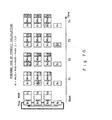
- Figure 9A illustrates a sixth embodiment of the present invention which multiplies a band matrix and a vector.
- like reference characters are used to designate corresponding parts to those in Figure 4A.
- the present embodiment uses m data processing units 1 each having two inputs and functions of multiplication and accumulation of the result of multiplication, n trays 2 and input data supply means connected to the data processing units.
- the calculation is performed in accordance with the procedure shown in Figure 9B and timing steps shown in Figures 9C and 9D.
- the multiplication of the band matrix with a width of k and the vector can be carried out in a process time proportional to k.
- Important things in the present embodiment are not to cause the vector to make one circulation and, unlike the first embodiment and so on, to shift the vector just to the position in which the band starts when setting the vector in the shift register 3. That is, where a process is started from the position in which the band starts, if calculation of sum of products while shifting the vector in a direction, the process will be terminated in a time proportional to k. However, where the process is initiated from the middle of the band due to some circumstances though not shown, it is evident that the vector has only to be shifted to an end initially. In this case, it is significant that the shift register 3 can be shifted in two directions.
- the vector is initially shifted right by k/2 (omission of decimals) and subsequently the calculation of sum of products is performed while the vector is ) shifted in the opposite direction (left in this case) so that the process is terminated in a time proportional to 3/2 k.
- the shift register 3 is not bi-directional, the vector has to be circulated by one rotation through the register.
- a time proportional to not the width k of the band matrix but its magnitude n is needed.
- the difference is very great. It is an advantage of the present invention that the multiplication of a band matrix and a vector can be carried out in a time proportional to the width k of the band matrix.
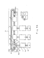
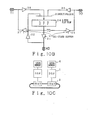
- Figure 10A illustrates a specific structure of the tray.
- the tray is basically a one-word latch. Access to the tray from DSP and data transfer from a tray to the next can be carried out in one cycle (post shift).
- Switching between functions is made by lower bits of an address line simultaneously with data access, 5 improving the speed of operation.
- One tray is a gate array of a scale of about 1200 basic cells. Two, three or four trays can be packaged in one chip.
- the tray can incorporate work registers for several words.
- a tray circuit 2 is shown in Figure 10B. It comprises a bus interface circuit comprising a tri-state buffer 31 and a buffer 32, a multiplexer 33, a D-type flip-flop 34, a first interface circuit comprising a tri-state buffer 35 and a buffer 36, and a second interface circuit comprising a tri-state buffer 37 and a buffer 38.
- the output of tri-state buffer 31 is connected to data processing unit 1 and the input of buffer 32 is also connected to the data processing unit 1.
- the output of tri-state buffer 35 and the input of buffer 36 are connected to the adjacent tray on the right side.
- the output of buffer 37 is connected to the adjacent tray on the left side and the input of buffer 38 is connected to the adjacent tray on the left side.
- the outputs of buffers 32, 36 and 38 are selected by multiplexer 33 to provide an output to D flip-flop 34.
- the output of D flip-flop 34 is connected to the input of tri-state buffers 31, 35 and 37.
- the data from the adjacent tray on the left side is input to D flip-flop 34 through buffer 38, output to the adjacent tray on the right side and applied to the data processing unit through tri-state buffer 31.
- the input from the adjacent tray on the right side is applied to the D flip-flop 34 through buffer 36, to the adjacent tray on the left side through tri-state buffer 37 and to the data processing unit 1 through tri-state buffer 31.
- Tray circuit 2 is connected to the adjacent tray as shown in Figure 10C, thereby forming a ring-bus comprising 32 bits, for example.
- the instruction for the tray is comprised by using the lower 2 bits of the address bus of the DSP forming the data processing unit 1 and an access mode signal (XR-W) of the DSP.
- the tray circuit 2 can be observed as a mere external register by the data processing unit comprising the DSP. Thus, the operation can be carried out without loading an overhead to the DSP.
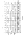
- the manner of bus access by the tray circuit and the DHP is shown in the timing chart of Figure 10D.
- the instructions for the tray circuit 2 comprise NOP, RSR (read and shift right), RSL (read and shift left), WSR (write and shift right), WSL (write and shift left), RD (read), and WR (write).
- Data flow between the tray circuit 2 and the data processing unit 1 is shown in Figure 10E.
- Signal X2 is a clock signal provided to DSP and signal H1 is obtained by dividing a frequency of signal X2 and corresponds to a machine cicyle of the DSP and the timing of the operation of DSP is based on the signal H1.
- Signal MSTRB shows a memory strobe signal and the later recited signals XR_W, XA and XD are valid during the period when the signal MSTRB is low.
- X attached to the head of respective signals XR_W, XA, XD, XRDY means "extended” and distinguishes a port of DSP to which a tray is connected. A port to which a memory is connected is not attached with X.
- Signal XR W is a control signal designating "read” when it is high and designating "write” when it is low.
- XA designates an address and XD designates a data signal.
- XRDY is a signal which a connected apparatus returns to the DSP but is not important for the present invention and the explanation is abbreviated.
- XA represents that XA output from the DSP is subject to sample and hold operation at a negative edge of MSTRB and operates as a control signal of an operation mode of the tray for an operation of a shifting of the tray.
- TD, TI and TO are respectively an abbreviation of tray data, tray in and tray out.
- TD is an output of DFF when the tray is shifted to the rightward, namely, data is shifted from left to right, the left side is TI, and the right side is TO. Conversely, when the tray is shifted to the left, the right side is TI and the left side is TO.
- the timing chart comprises three cycles of WSR1, WSR2 and RSR.
- the first WSR cycle (WSR1) is from to T1 to T5
- the second WSR cycle (WSR2) is from T5 to T11
- RSR cycle is from T11 to T13.
- Data(n), Instruction (n-1) and Data (n + 1) positioned at the starting of the timing chart in Figure 10D do not have any special meaning and merely designate a kind of data.
- T6 shifting operation starts and Data(x-1) on T1 is storerd in DFF and the value is output to TO. Simultaneously, Data(x-2) is supplied from the left side to TI. At this T6, XA of WSR2 cycle which starts at T5 is output. The operation from T5 to T9 is performed in the same way as T1 to T5.
- the RSR cycle starts and when read cycle follows immediately after the write cycle, the write cycle is extented by one machine cycle until it covers T11. During this extended cycle, XR - W becomes high at T10 and thereafter it is designated that the operation is in read cycle.
- Instruction(n + 2) designating RSR cycle is output on XA and sequentially Data(y-1) on DFF is output on XD.
- DSP reads this data at T13 and sequentially a shifting operation starts. Data(y-2) on T1. is latched at DFF and simultaneously is output to TO. At this time, Data(y-3) from the left side appears on TI.
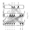
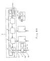
- Figure 11 is a block diagram of a neuro-computer actually configured using the embodiments of the present invention.
- the basic configuration of the present invention is an SIMD type multiprocessor using one-dimensional torus coupling of DSPs.
- the trays connected to the DSPs through bi-directional buses are latches having a transfer function and connected together in the form of a ring to form a cyclic shift register.
- the shift register is referred to as the ring.
- Each DSP has a 2K-word internal memory and a 64-word built-on RAM.
- the internal memory can be accessed in one cycle and the built-on memory can be accessed in 1 or 2 cycles.
- the built-on RAM is connected to a VMEW bus of a host computer through a common bus for initial loading of a program and data. External inputs are also connected to the host computer through a buffer memory.
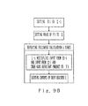
- Figure 12 is a time-space chart at the time of learning in the embodiments of the present invention.
- the number of processors is represented in the longitudinal direction, and time is represented in the lateral direction.
- I corresponds to the number of processors of an input layer
- H corresponds to the number of processors of a hidden layer
- T corresponds to time of calculation of sum of products.
- the time required to calculate the forward sum of products of the hidden layer is proportional to the product of the number of processors in the input layer and the operational time T of one processor corresponding to the sum of products.
- the sigmoid is calculated.
- the forward sum of products (2H T ) and the sigmoid of the output layer are calculated. Since the number of processors in the output layer is smaller than the number of processors in the hidden layer, the size of the ring also becomes small.
- a teacher signal input is received to calculate and back propagate an error.
- the error calculation is performed by a backward operation of the sum of the products in the output layer, and the weight updating in the output layer is performed through gradient vector calculation and lowpass filtering.
Applications Claiming Priority (8)
| Application Number | Priority Date | Filing Date | Title |
|---|---|---|---|
| JP1243969A JPH03105581A (ja) | 1989-09-20 | 1989-09-20 | 並列データ処理方式 |
| JP1243972A JP2825133B2 (ja) | 1989-09-20 | 1989-09-20 | 並列データ処理方式 |
| JP1243971A JPH03105583A (ja) | 1989-09-20 | 1989-09-20 | 並列データ処理方式 |
| JP243970/89 | 1989-09-20 | ||
| JP243972/89 | 1989-09-20 | ||
| JP243971/89 | 1989-09-20 | ||
| JP1243970A JPH03105582A (ja) | 1989-09-20 | 1989-09-20 | 並列データ処理方式 |
| JP243969/89 | 1989-09-20 |
Publications (3)
| Publication Number | Publication Date |
|---|---|
| EP0421639A2 true EP0421639A2 (fr) | 1991-04-10 |
| EP0421639A3 EP0421639A3 (en) | 1993-08-04 |
| EP0421639B1 EP0421639B1 (fr) | 1998-04-22 |
Family
ID=27477938
Family Applications (1)
| Application Number | Title | Priority Date | Filing Date |
|---|---|---|---|
| EP90310302A Expired - Lifetime EP0421639B1 (fr) | 1989-09-20 | 1990-09-20 | Système de traitement de données en parallèle |
Country Status (4)
| Country | Link |
|---|---|
| US (1) | US5600843A (fr) |
| EP (1) | EP0421639B1 (fr) |
| AU (1) | AU641418B2 (fr) |
| DE (1) | DE69032259T2 (fr) |
Cited By (1)
| Publication number | Priority date | Publication date | Assignee | Title |
|---|---|---|---|---|
| DE4417932A1 (de) * | 1993-06-18 | 1994-12-22 | Fujitsu Ltd | Paralleldatenverarbeitungssystem |
Families Citing this family (27)
| Publication number | Priority date | Publication date | Assignee | Title |
|---|---|---|---|---|
| US6157611A (en) * | 1998-08-18 | 2000-12-05 | Qualcomm Inc. | Method and apparatus for transmission and construction of quasi orthogonal vectors |
| US6816593B1 (en) * | 1999-12-23 | 2004-11-09 | Ati International Srl | Method and apparatus for transposing bits |
| US6993764B2 (en) * | 2000-06-30 | 2006-01-31 | The Regents Of The University Of California | Buffered coscheduling for parallel programming and enhanced fault tolerance |
| US6901422B1 (en) * | 2001-03-21 | 2005-05-31 | Apple Computer, Inc. | Matrix multiplication in a vector processing system |
| US7478222B2 (en) * | 2005-03-29 | 2009-01-13 | Karl M. Fant | Programmable pipeline array |
| US20090132792A1 (en) * | 2007-11-15 | 2009-05-21 | Dennis Arthur Ruffer | Method of generating internode timing diagrams for a multiprocessor array |
| US8175853B2 (en) * | 2008-03-28 | 2012-05-08 | International Business Machines Corporation | Systems and methods for a combined matrix-vector and matrix transpose vector multiply for a block-sparse matrix |
| US9015093B1 (en) | 2010-10-26 | 2015-04-21 | Michael Lamport Commons | Intelligent control with hierarchical stacked neural networks |
| US8775341B1 (en) | 2010-10-26 | 2014-07-08 | Michael Lamport Commons | Intelligent control with hierarchical stacked neural networks |
| JP5680466B2 (ja) | 2011-03-29 | 2015-03-04 | 三菱重工業株式会社 | 並列処理システム及び並列処理システムの動作方法 |
| CN103168289B (zh) * | 2011-10-14 | 2016-07-06 | 松下知识产权经营株式会社 | 转置运算装置及其集成电路、以及转置处理方法 |
| US8918351B2 (en) * | 2012-07-30 | 2014-12-23 | International Business Machines Corporation | Providing transposable access to a synapse array using column aggregation |
| US9218564B2 (en) | 2012-07-30 | 2015-12-22 | International Business Machines Corporation | Providing transposable access to a synapse array using a recursive array layout |
| US11494653B2 (en) | 2014-03-06 | 2022-11-08 | Progress, Inc. | Neural network and method of neural network training |
| EP3035249B1 (fr) * | 2014-12-19 | 2019-11-27 | Intel Corporation | Procédé et appareil de calcul coopératif et distribué dans des réseaux neuronaux artificiels |
| EP3469521A4 (fr) * | 2016-06-09 | 2020-02-26 | Progress, Inc. | Réseau neuronal et procédé d'apprentissage de réseau neuronal |
| US11657267B2 (en) * | 2016-07-21 | 2023-05-23 | Denso It Laboratory, Inc. | Neural network apparatus, vehicle control system, decomposition device, and program |
| KR20240024356A (ko) * | 2017-06-21 | 2024-02-23 | 가부시키가이샤 한도오따이 에네루기 켄큐쇼 | 뉴럴 네트워크를 가지는 반도체 장치 |
| US11409692B2 (en) | 2017-07-24 | 2022-08-09 | Tesla, Inc. | Vector computational unit |
| US11157441B2 (en) | 2017-07-24 | 2021-10-26 | Tesla, Inc. | Computational array microprocessor system using non-consecutive data formatting |
| US10671349B2 (en) | 2017-07-24 | 2020-06-02 | Tesla, Inc. | Accelerated mathematical engine |
| US11157287B2 (en) | 2017-07-24 | 2021-10-26 | Tesla, Inc. | Computational array microprocessor system with variable latency memory access |
| US11893393B2 (en) | 2017-07-24 | 2024-02-06 | Tesla, Inc. | Computational array microprocessor system with hardware arbiter managing memory requests |
| GB2568230B (en) * | 2017-10-20 | 2020-06-03 | Graphcore Ltd | Processing in neural networks |
| US11373088B2 (en) * | 2017-12-30 | 2022-06-28 | Intel Corporation | Machine learning accelerator mechanism |
| US11561791B2 (en) | 2018-02-01 | 2023-01-24 | Tesla, Inc. | Vector computational unit receiving data elements in parallel from a last row of a computational array |
| CN109272112B (zh) * | 2018-07-03 | 2021-08-27 | 北京中科睿芯科技集团有限公司 | 一种面向神经网络的数据重用指令映射方法、系统及装置 |
Citations (3)
| Publication number | Priority date | Publication date | Assignee | Title |
|---|---|---|---|---|
| US4524455A (en) * | 1981-06-01 | 1985-06-18 | Environmental Research Inst. Of Michigan | Pipeline processor |
| EP0147857A2 (fr) * | 1983-12-28 | 1985-07-10 | Hitachi, Ltd. | Système de traitement de données en parallèle |
| EP0236762A1 (fr) * | 1986-03-08 | 1987-09-16 | Hitachi, Ltd. | Système à multiprocesseur |
Family Cites Families (7)
| Publication number | Priority date | Publication date | Assignee | Title |
|---|---|---|---|---|
| US4816993A (en) * | 1984-12-24 | 1989-03-28 | Hitachi, Ltd. | Parallel processing computer including interconnected operation units |
| EP0269995B1 (fr) * | 1986-11-27 | 1993-06-23 | Nippon Telegraph And Telephone Corporation | Dispositif et méthode pour le traitement parallél de données |
| US5165023A (en) * | 1986-12-17 | 1992-11-17 | Massachusetts Institute Of Technology | Parallel processing system with processor array and network communications system for transmitting messages of variable length |
| US4891787A (en) * | 1986-12-17 | 1990-01-02 | Massachusetts Institute Of Technology | Parallel processing system with processor array having SIMD/MIMD instruction processing |
| US5129092A (en) * | 1987-06-01 | 1992-07-07 | Applied Intelligent Systems,Inc. | Linear chain of parallel processors and method of using same |
| US5014235A (en) * | 1987-12-15 | 1991-05-07 | Steven G. Morton | Convolution memory |
| FR2635390B1 (fr) * | 1988-08-12 | 1990-10-12 | Bull Sa | Unite centrale pour systeme de traitement de l'information |
-
1990
- 1990-09-20 DE DE69032259T patent/DE69032259T2/de not_active Expired - Fee Related
- 1990-09-20 AU AU63030/90A patent/AU641418B2/en not_active Ceased
- 1990-09-20 EP EP90310302A patent/EP0421639B1/fr not_active Expired - Lifetime
-
1994
- 1994-04-14 US US08/227,472 patent/US5600843A/en not_active Expired - Fee Related
Patent Citations (3)
| Publication number | Priority date | Publication date | Assignee | Title |
|---|---|---|---|---|
| US4524455A (en) * | 1981-06-01 | 1985-06-18 | Environmental Research Inst. Of Michigan | Pipeline processor |
| EP0147857A2 (fr) * | 1983-12-28 | 1985-07-10 | Hitachi, Ltd. | Système de traitement de données en parallèle |
| EP0236762A1 (fr) * | 1986-03-08 | 1987-09-16 | Hitachi, Ltd. | Système à multiprocesseur |
Non-Patent Citations (2)
| Title |
|---|
| IEEE INTERNATIONAL CONFERENCE ON NEURAL NETWORKS vol. 2, 24 July 1988, SAN DIEGO , USA pages 165 - 172 KUNG 'Parallel architectures for artificial neural nets' * |
| NEURAL NETWORKS FROM MODELS TO APPLICATIONS E.S.P.C.I. June 1988, PARIS , FRANCE pages 682 - 691 PERSONNAZ 'Towards a neural network chip : A performance assessment and a simple example' * |
Cited By (3)
| Publication number | Priority date | Publication date | Assignee | Title |
|---|---|---|---|---|
| DE4417932A1 (de) * | 1993-06-18 | 1994-12-22 | Fujitsu Ltd | Paralleldatenverarbeitungssystem |
| US5627944A (en) * | 1993-06-18 | 1997-05-06 | Fujitsu Limited | Parallel data processing system |
| DE4417932B4 (de) * | 1993-06-18 | 2005-07-28 | Fujitsu Ltd., Kawasaki | Verfahren und ein System zum Erhalten von Zieleinstellbeträgen für Ausführungsparameter durch Lernen einer Mehrzahl von Sätzen von Muster-Eingabedaten und Muster-Ausgabedaten |
Also Published As
| Publication number | Publication date |
|---|---|
| DE69032259D1 (de) | 1998-05-28 |
| DE69032259T2 (de) | 1998-08-13 |
| EP0421639A3 (en) | 1993-08-04 |
| US5600843A (en) | 1997-02-04 |
| AU641418B2 (en) | 1993-09-23 |
| EP0421639B1 (fr) | 1998-04-22 |
| AU6303090A (en) | 1991-03-28 |
Similar Documents
| Publication | Publication Date | Title |
|---|---|---|
| US5600843A (en) | Ring systolic array system for synchronously performing matrix/neuron computation using data transferred through cyclic shift register connected in cascade of trays | |
| US5506998A (en) | Parallel data processing system using a plurality of processing elements to process data and a plurality of trays connected to some of the processing elements to store and transfer data | |
| US5544336A (en) | Parallel data processing system which efficiently performs matrix and neurocomputer operations, in a negligible data transmission time | |
| US5517600A (en) | Neuro-chip and neurocomputer having the chip | |
| CN107341547B (zh) | 一种用于执行卷积神经网络训练的装置和方法 | |
| US5617512A (en) | Triangular scalable neural array processor | |
| EP3451236A1 (fr) | Procédé et dispositif d'exécution d'une opération de transfert d'un réseau neuronal en couches entièrement connecté | |
| US20210241071A1 (en) | Architecture of a computer for calculating a convolution layer in a convolutional neural network | |
| EP0422348A2 (fr) | Réseau systolique à deux dimensions pour réseaux neuroneaux, et méthode | |
| US5608844A (en) | Neural processor comprising distributed synaptic cells | |
| Lin et al. | Algorithmic mapping of neural network models onto parallel SIMD machines | |
| US11017290B2 (en) | Signal processing module, especially for a neural network and a neuronal circuit | |
| US5146543A (en) | Scalable neural array processor | |
| US5065339A (en) | Orthogonal row-column neural processor | |
| US5148515A (en) | Scalable neural array processor and method | |
| JPH02193251A (ja) | エラー後方伝ぱん法と神経網システム | |
| CN110580519A (zh) | 一种卷积运算结构及其方法 | |
| CN110689123A (zh) | 基于脉动阵列的长短期记忆神经网络前向加速系统及方法 | |
| JPH06502265A (ja) | 信号処理におけるマトリクス演算の計算回路装置 | |
| JPH07271748A (ja) | データを正規化する手段を含むニューラル・プロセッサ | |
| US5627944A (en) | Parallel data processing system | |
| JP2825133B2 (ja) | 並列データ処理方式 | |
| JP7251354B2 (ja) | 情報処理装置、情報処理プログラム、及び情報処理方法 | |
| JPH03105583A (ja) | 並列データ処理方式 | |
| US20220036196A1 (en) | Reconfigurable computing architecture for implementing artificial neural networks |
Legal Events
| Date | Code | Title | Description |
|---|---|---|---|
| PUAI | Public reference made under article 153(3) epc to a published international application that has entered the european phase |
Free format text: ORIGINAL CODE: 0009012 |
|
| AK | Designated contracting states |
Kind code of ref document: A2 Designated state(s): DE FR GB |
|
| PUAL | Search report despatched |
Free format text: ORIGINAL CODE: 0009013 |
|
| AK | Designated contracting states |
Kind code of ref document: A3 Designated state(s): DE FR GB |
|
| 17P | Request for examination filed |
Effective date: 19940127 |
|
| 17Q | First examination report despatched |
Effective date: 19960402 |
|
| GRAG | Despatch of communication of intention to grant |
Free format text: ORIGINAL CODE: EPIDOS AGRA |
|
| GRAG | Despatch of communication of intention to grant |
Free format text: ORIGINAL CODE: EPIDOS AGRA |
|
| GRAH | Despatch of communication of intention to grant a patent |
Free format text: ORIGINAL CODE: EPIDOS IGRA |
|
| GRAH | Despatch of communication of intention to grant a patent |
Free format text: ORIGINAL CODE: EPIDOS IGRA |
|
| GRAA | (expected) grant |
Free format text: ORIGINAL CODE: 0009210 |
|
| AK | Designated contracting states |
Kind code of ref document: B1 Designated state(s): DE FR GB |
|
| REF | Corresponds to: |
Ref document number: 69032259 Country of ref document: DE Date of ref document: 19980528 |
|
| ET | Fr: translation filed | ||
| PLBE | No opposition filed within time limit |
Free format text: ORIGINAL CODE: 0009261 |
|
| STAA | Information on the status of an ep patent application or granted ep patent |
Free format text: STATUS: NO OPPOSITION FILED WITHIN TIME LIMIT |
|
| 26N | No opposition filed | ||
| REG | Reference to a national code |
Ref country code: GB Ref legal event code: IF02 |
|
| PGFP | Annual fee paid to national office [announced via postgrant information from national office to epo] |
Ref country code: FR Payment date: 20050823 Year of fee payment: 16 |
|
| PGFP | Annual fee paid to national office [announced via postgrant information from national office to epo] |
Ref country code: GB Payment date: 20050914 Year of fee payment: 16 |
|
| PGFP | Annual fee paid to national office [announced via postgrant information from national office to epo] |
Ref country code: DE Payment date: 20050915 Year of fee payment: 16 |
|
| PG25 | Lapsed in a contracting state [announced via postgrant information from national office to epo] |
Ref country code: DE Free format text: LAPSE BECAUSE OF NON-PAYMENT OF DUE FEES Effective date: 20070403 |
|
| GBPC | Gb: european patent ceased through non-payment of renewal fee |
Effective date: 20060920 |
|
| REG | Reference to a national code |
Ref country code: FR Ref legal event code: ST Effective date: 20070531 |
|
| PG25 | Lapsed in a contracting state [announced via postgrant information from national office to epo] |
Ref country code: GB Free format text: LAPSE BECAUSE OF NON-PAYMENT OF DUE FEES Effective date: 20060920 |
|
| PG25 | Lapsed in a contracting state [announced via postgrant information from national office to epo] |
Ref country code: FR Free format text: LAPSE BECAUSE OF NON-PAYMENT OF DUE FEES Effective date: 20061002 |