EP0419021A2 - Sensors with vibrating elements - Google Patents
Sensors with vibrating elements Download PDFInfo
- Publication number
- EP0419021A2 EP0419021A2 EP90308586A EP90308586A EP0419021A2 EP 0419021 A2 EP0419021 A2 EP 0419021A2 EP 90308586 A EP90308586 A EP 90308586A EP 90308586 A EP90308586 A EP 90308586A EP 0419021 A2 EP0419021 A2 EP 0419021A2
- Authority
- EP
- European Patent Office
- Prior art keywords
- sensor
- excitation signal
- diaphragm
- region
- applying
- Prior art date
- Legal status (The legal status is an assumption and is not a legal conclusion. Google has not performed a legal analysis and makes no representation as to the accuracy of the status listed.)
- Ceased
Links
Images
Classifications
-
- G—PHYSICS
- G01—MEASURING; TESTING
- G01D—MEASURING NOT SPECIALLY ADAPTED FOR A SPECIFIC VARIABLE; ARRANGEMENTS FOR MEASURING TWO OR MORE VARIABLES NOT COVERED IN A SINGLE OTHER SUBCLASS; TARIFF METERING APPARATUS; MEASURING OR TESTING NOT OTHERWISE PROVIDED FOR
- G01D3/00—Indicating or recording apparatus with provision for the special purposes referred to in the subgroups
- G01D3/028—Indicating or recording apparatus with provision for the special purposes referred to in the subgroups mitigating undesired influences, e.g. temperature, pressure
- G01D3/036—Indicating or recording apparatus with provision for the special purposes referred to in the subgroups mitigating undesired influences, e.g. temperature, pressure on measuring arrangements themselves
-
- G—PHYSICS
- G01—MEASURING; TESTING
- G01L—MEASURING FORCE, STRESS, TORQUE, WORK, MECHANICAL POWER, MECHANICAL EFFICIENCY, OR FLUID PRESSURE
- G01L9/00—Measuring steady of quasi-steady pressure of fluid or fluent solid material by electric or magnetic pressure-sensitive elements; Transmitting or indicating the displacement of mechanical pressure-sensitive elements, used to measure the steady or quasi-steady pressure of a fluid or fluent solid material, by electric or magnetic means
- G01L9/0001—Transmitting or indicating the displacement of elastically deformable gauges by electric, electro-mechanical, magnetic or electro-magnetic means
- G01L9/0008—Transmitting or indicating the displacement of elastically deformable gauges by electric, electro-mechanical, magnetic or electro-magnetic means using vibrations
- G01L9/0019—Transmitting or indicating the displacement of elastically deformable gauges by electric, electro-mechanical, magnetic or electro-magnetic means using vibrations of a semiconductive element
- G01L9/002—Optical excitation or measuring
-
- G—PHYSICS
- G01—MEASURING; TESTING
- G01L—MEASURING FORCE, STRESS, TORQUE, WORK, MECHANICAL POWER, MECHANICAL EFFICIENCY, OR FLUID PRESSURE
- G01L9/00—Measuring steady of quasi-steady pressure of fluid or fluent solid material by electric or magnetic pressure-sensitive elements; Transmitting or indicating the displacement of mechanical pressure-sensitive elements, used to measure the steady or quasi-steady pressure of a fluid or fluent solid material, by electric or magnetic means
- G01L9/0001—Transmitting or indicating the displacement of elastically deformable gauges by electric, electro-mechanical, magnetic or electro-magnetic means
- G01L9/0008—Transmitting or indicating the displacement of elastically deformable gauges by electric, electro-mechanical, magnetic or electro-magnetic means using vibrations
- G01L9/0022—Transmitting or indicating the displacement of elastically deformable gauges by electric, electro-mechanical, magnetic or electro-magnetic means using vibrations of a piezoelectric element
- G01L9/0023—Optical excitation or measuring
-
- Y—GENERAL TAGGING OF NEW TECHNOLOGICAL DEVELOPMENTS; GENERAL TAGGING OF CROSS-SECTIONAL TECHNOLOGIES SPANNING OVER SEVERAL SECTIONS OF THE IPC; TECHNICAL SUBJECTS COVERED BY FORMER USPC CROSS-REFERENCE ART COLLECTIONS [XRACs] AND DIGESTS
- Y10—TECHNICAL SUBJECTS COVERED BY FORMER USPC
- Y10S—TECHNICAL SUBJECTS COVERED BY FORMER USPC CROSS-REFERENCE ART COLLECTIONS [XRACs] AND DIGESTS
- Y10S73/00—Measuring and testing
- Y10S73/01—Vibration
Definitions
- This invention relates to sensors, and is more particularly but not exclusively concerned with sensors in which the parameter to be sensed affects the frequency of a resonantly vibrating element whose resonant vibration is excited and/or sensed optically.
- the sensor of this prior proposal suffers from the disadvantage that the characteristics of the sensing element are not very stable or repeatable, firstly because the silicon dioxide material of the sensing element is amorphous and secondly because of the difficulty of producing a uniform and repeatable gold coating on such an amorphous sensing element.
- metal coating can result in a very large and rather unpredictable temperature coefficient.
- a sensor comprising a resonantly vibratable element formed as part of a unitary semiconductor structure which is arranged such that a measurand applied to the structure affects the resonant frequency of the vibratable element, and means for applying an excitation signal to the sensor to excite resonant vibration of said element, wherein said excitation signal applying means is arranged to excite said element indirectly by applying said excitation signal to a region of the structure other than said element.
- the excitation signal applying means may comprise means for applying an electrical signal to a resistor or piezoelectric device formed in said region, whereby to produce vibration-inducing stresses in said region by local heating or piezoelectric effect respectively.
- the excitation signal applying means may comprise means for applying an optical excitation signal to said region.
- said region is preferably provided with a coating for absorbing said optical excitation signal, for example a coating of a metal such as aluminium, chromium or gold, or a coating of a material exhibiting surface piezoelectric effect, such as zinc oxide.
- Said semiconductor structure may conveniently be made from silicon, preferably single crystal silicon.
- the semiconductor structure includes a diaphragm, and said element comprises a beam arranged to have the tension therein varied by flexing of the diaphragm in response to changes in pressure applied to the diaphragm, whereby the sensor serves as a pressure sensor.
- said region of the structure may be on one surface of the diaphragm, or adjacent one end of the beam.
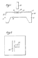
- the sensor of Figure 1 is indicated generally at 10, and is basically similar to the sensor described in detail in United States Patent Application Serial No. 358,771 (Barth et al), filed on 30 May 1989.
- the sensor 10 comprises first and second single crystal silicon wafers 12, 14, of which the first wafer has a beam 16 formed therein by cutting two parallel slots therethrough to define the two longitudinally-extending sides of the beam, while the second has a diaphragm 18 with a trench 20 in its upper surface formed therein by electrochemical etching.
- the two wafers 12, 14 are fusion bonded together at the dotted line 22, to form a unitary structure 24 in which the beam 16 is disposed above the trench 20 in the diaphragm 18, as described in the aforementioned United States patent application.
- the unitary silicon structure 24 is sealed in a suitable housing (not shown), with the upper surface of the diaphragm 18 facing into an evacuated chamber within the housing.
- the beam 16 is excited into resonant vibration, and a pressure to be sensed is admitted to the housing beneath the diaphragm 18, so that the diaphragm flexes in dependence on the pressure, and thus varies the tension in, and therefore the resonant frequency of, the beam.
- resonant vibration of the beam 16 can be optically excited by directing a suitable pulsed optical excitation signal, via an optical fibre 26 which passes sealingly through the aforementioned evacuated chamber and terminates immediately above the beam, onto an optically absorptive coating 28 of a suitable metal, eg aluminium, chromium or gold, deposited, typically by sputtering, on the upper surface of the diaphragm 18 in the base of the trench 20, at the position indicated at B in Figure 1.
- a suitable metal eg aluminium, chromium or gold
- the beam 16 does not require to be coated and therefore consists solely of single crystal silicon, it has a very high Q and its vibration characteristics are very stable and repeatable: in particular, its temperature coefficient is much lower than that of a coated beam, and much more predictable and stable.
- the coating 28 is deposited at B, it forms with the underside of the beam 16 a Fabry-Perot optical cavity, which can be used if desired to sense the frequency of vibration of the beam.
- the coating 28 can be deposited at the position indicated at D in Figure 1, adjacent one end of the beam 16 (which would clearly necessitate relocating the optical fibre 26), or at the position indicated at A in Figure 1, on the underside of the diaphragm 18.
- a coating of a material exhibiting surface piezoelectric effect eg zinc oxide, can be used.
- Figure 2 is a plan view of such an arrangement, with a first beam 30 substantially identical to the beam 16 of Figure 1 (ie arranged to be tensioned by an associated diaphragm not shown in Figure 2), and a second, cantilever beam 32, disposed at right angles to the first beam.
- the beam 32 is formed in the same cutting operation as is used to form the beam 30, and is used for temperature compensation purposes as described in more detail in our co-pending United Kingdom Patent Application No. 8822877.0.
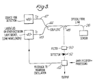
- an excitation light source 40 typically a laser diode or an LED which produces an optical output at a first wavelength l1 of about 1300nm
- an amplifier 42 to produce a pulsed optical excitation signal at a frequency approximately equal to the expected resonant frequency of the beam 16 in the sensor 10.
- the output of the source 40 is coupled via an optical fibre 43 and one input port of an optical coupler 44 into the optical fibre 26, along with a continuous optical signal, of lower wavelength l2, which is produced by a source 46, typically an LED, and applied via an optical fibre 47, to another input port of the coupler 44.
- the pulsed optical output signal of wavelength l1 exits the end of the optical fibre 26, and is incident upon and absorbed by the coating 28, thus creating localised thermal stress which excites the diaphragm 18 into vibration and thereby indirectly exciting the beam 16 into resonant vibration.
- the optical signal of wavelength l2 is modulated by the resonantly vibrating beam 16 in the sensor 10, and reflected back along the optical fibre 26 to a splitter 48, and thence through a Fabry-Perot or like filter 50 to a photoelectric detector 52.
- the output of the detector 52 which contains a component at the resonant frequency of the beam 16, is applied to the input of the amplifier 42 to create a positive feedback loop, which adjusts the operating frequency of the source 40 so as to maintain the beam vibrating at its resonant frequency, while a secondary output from the amplifier 42, again containing a component at the resonant frequency of the beam 16, constitutes the pressure dependent output of the system.
- suitable optically absorbent coatings other than metal or a piezoelectric material can be used to absorb the optical excitation signal: indeed, in the limit, the coating may be omitted altogether, particularly if an especially sensitive part of the structure 24 (other than the beam 16) is located and/or slightly more optical power is used.
- the beam 16 can be indirectly excited into resonant vibration by excitation signals other than an optical excitation signal.
- the optical excitation signal is believed to work by creating vibration-inducing stresses resulting from local heating due to absorption of the light constituting the optical signal (which stresses are enhanced or supplanted by stresses due to piezoelectric effect when the absorptive coating 28 exhibits surface piezoelectric effect). Similar local heating and/or piezoelectric effects can be created by forming a resistor or piezoelectric resistor in the wafer 12 or the wafer 14 at a location corresponding to a respective one of the locations A, B, D specified for the coating 28.
- This resistor can be formed as described in the aforementioned United States patent application, and would enable resonant vibration of the beam 16 to be excited by an electrical excitation signal, rather than an optical one.
- the vibrations can still be sensed optically, if desired: however, they can alternatively be sensed electrically, for example by means of piezoresistors, as described in the aforementioned United States patent application.
Abstract
Description
- This invention relates to sensors, and is more particularly but not exclusively concerned with sensors in which the parameter to be sensed affects the frequency of a resonantly vibrating element whose resonant vibration is excited and/or sensed optically.
- It has already been proposed, in a letter entitled "Optically Activated Vibrations in a Micromachined Silica Structure" by S. Venkatesh and B. Culshaw (Electronics Letters, 11 April 1985, Vol. 21, No. 8), to provide a sensor comprising a microminiature bridge of silicon dioxide, fabricated using anisotropic etch techniques on a silicon substrate. A thin gold film is sputtered onto the bridge, which is then excited into resonant vibration, typically at about 260 KHz, by directing a suitably modulated laser beam onto the centre of the bridge. The frequency of vibration of the bridge is detected using another laser beam. The sensor is arranged such that the parameter to be sensed acts on the substrate so as to vary the resonant frequency of the bridge.
- The sensor of this prior proposal suffers from the disadvantage that the characteristics of the sensing element are not very stable or repeatable, firstly because the silicon dioxide material of the sensing element is amorphous and secondly because of the difficulty of producing a uniform and repeatable gold coating on such an amorphous sensing element. In particular, metal coating can result in a very large and rather unpredictable temperature coefficient.
- It is therefore an object of the present invention to provide a sensor in which the abovementioned disadvantage is significantly alleviated.
- According to the present invention, there is provided a sensor comprising a resonantly vibratable element formed as part of a unitary semiconductor structure which is arranged such that a measurand applied to the structure affects the resonant frequency of the vibratable element, and means for applying an excitation signal to the sensor to excite resonant vibration of said element, wherein said excitation signal applying means is arranged to excite said element indirectly by applying said excitation signal to a region of the structure other than said element.
- The excitation signal applying means may comprise means for applying an electrical signal to a resistor or piezoelectric device formed in said region, whereby to produce vibration-inducing stresses in said region by local heating or piezoelectric effect respectively.
- Alternatively and preferably, the excitation signal applying means may comprise means for applying an optical excitation signal to said region. In this case said region is preferably provided with a coating for absorbing said optical excitation signal, for example a coating of a metal such as aluminium, chromium or gold, or a coating of a material exhibiting surface piezoelectric effect, such as zinc oxide. Said semiconductor structure may conveniently be made from silicon, preferably single crystal silicon.
- In a preferred embodiment of the invention, the semiconductor structure includes a diaphragm, and said element comprises a beam arranged to have the tension therein varied by flexing of the diaphragm in response to changes in pressure applied to the diaphragm, whereby the sensor serves as a pressure sensor. In that case, said region of the structure may be on one surface of the diaphragm, or adjacent one end of the beam.
- The invention will now be described, by way of example only, with reference to the accompanying drawings, of which:
- Figure 1 shows somewhat schematically an optically excitable silicon pressure sensor in accordance with the present invention;
- Figure 2 is a plan view of a modified version of the sensor of Figure 1; and
- Figure 3 is a schematic diagram of a complete sensor system based upon the sensor of Figure 1.
- The sensor of Figure 1 is indicated generally at 10, and is basically similar to the sensor described in detail in United States Patent Application Serial No. 358,771 (Barth et al), filed on 30 May 1989. Thus the
sensor 10 comprises first and second single crystal silicon wafers 12, 14, of which the first wafer has abeam 16 formed therein by cutting two parallel slots therethrough to define the two longitudinally-extending sides of the beam, while the second has adiaphragm 18 with atrench 20 in its upper surface formed therein by electrochemical etching. The twowafers unitary structure 24 in which thebeam 16 is disposed above thetrench 20 in thediaphragm 18, as described in the aforementioned United States patent application. - To use the
sensor 10 as a pressure sensor, theunitary silicon structure 24 is sealed in a suitable housing (not shown), with the upper surface of thediaphragm 18 facing into an evacuated chamber within the housing. Thebeam 16 is excited into resonant vibration, and a pressure to be sensed is admitted to the housing beneath thediaphragm 18, so that the diaphragm flexes in dependence on the pressure, and thus varies the tension in, and therefore the resonant frequency of, the beam. - In the aforementioned United States patent application, the principal methods described for exciting the
beam 16 into resonant vibration and sensing the frequency of the resulting vibrations are electrostatic and piezoelectric respectively, although direct optical excitation, by applying pulses of light energy directly to the beam, is also disclosed. In accordance with prior art teachings, eg of the aforementioned letter by Venkatesh and Culshaw, this would typically have involved providing thebeam 16 with a metal coating, eg of gold, at the location indicated at C in Figure 1, with the disadvantage mentioned earlier. However, we have found that it is possible to excite thebeam 16 into resonant vibration indirectly, by directing the optical excitation signal at a region of theunitary structure 24 other than the beam. - Thus we have found that resonant vibration of the
beam 16 can be optically excited by directing a suitable pulsed optical excitation signal, via anoptical fibre 26 which passes sealingly through the aforementioned evacuated chamber and terminates immediately above the beam, onto an opticallyabsorptive coating 28 of a suitable metal, eg aluminium, chromium or gold, deposited, typically by sputtering, on the upper surface of thediaphragm 18 in the base of thetrench 20, at the position indicated at B in Figure 1. It will be noted that the optical excitation signal passes through thebeam 16, which can readily be achieved by using a signal whose wavelength is of the order of 1300nm, to which theunitary silicon structure 24 is substantially transparent. - Since the
beam 16 does not require to be coated and therefore consists solely of single crystal silicon, it has a very high Q and its vibration characteristics are very stable and repeatable: in particular, its temperature coefficient is much lower than that of a coated beam, and much more predictable and stable. - With the
coating 28 is deposited at B, it forms with the underside of the beam 16 a Fabry-Perot optical cavity, which can be used if desired to sense the frequency of vibration of the beam. - As an alternative, the
coating 28 can be deposited at the position indicated at D in Figure 1, adjacent one end of the beam 16 (which would clearly necessitate relocating the optical fibre 26), or at the position indicated at A in Figure 1, on the underside of thediaphragm 18. Also, instead of an optically absorptive metal coating, a coating of a material exhibiting surface piezoelectric effect, eg zinc oxide, can be used. - We have also found that by exciting the
diaphragm 18, it is possible to indirectly excite two resonant elements, eg beams, simultaneously. Figure 2 is a plan view of such an arrangement, with afirst beam 30 substantially identical to thebeam 16 of Figure 1 (ie arranged to be tensioned by an associated diaphragm not shown in Figure 2), and a second,cantilever beam 32, disposed at right angles to the first beam. Thebeam 32 is formed in the same cutting operation as is used to form thebeam 30, and is used for temperature compensation purposes as described in more detail in our co-pending United Kingdom Patent Application No. 8822877.0. - The way in which the
sensor 10 is incorporated into a sensor system for sensing pressure is illustrated in Figure 3. Thus anexcitation light source 40, typically a laser diode or an LED which produces an optical output at a first wavelength l₁ of about 1300nm, is driven by anamplifier 42 to produce a pulsed optical excitation signal at a frequency approximately equal to the expected resonant frequency of thebeam 16 in thesensor 10. The output of thesource 40 is coupled via anoptical fibre 43 and one input port of anoptical coupler 44 into theoptical fibre 26, along with a continuous optical signal, of lower wavelength l₂, which is produced by asource 46, typically an LED, and applied via anoptical fibre 47, to another input port of thecoupler 44. - The pulsed optical output signal of wavelength l₁ exits the end of the
optical fibre 26, and is incident upon and absorbed by thecoating 28, thus creating localised thermal stress which excites thediaphragm 18 into vibration and thereby indirectly exciting thebeam 16 into resonant vibration. - The optical signal of wavelength l₂ is modulated by the resonantly vibrating
beam 16 in thesensor 10, and reflected back along theoptical fibre 26 to asplitter 48, and thence through a Fabry-Perot or like filter 50 to aphotoelectric detector 52. The output of thedetector 52, which contains a component at the resonant frequency of thebeam 16, is applied to the input of theamplifier 42 to create a positive feedback loop, which adjusts the operating frequency of thesource 40 so as to maintain the beam vibrating at its resonant frequency, while a secondary output from theamplifier 42, again containing a component at the resonant frequency of thebeam 16, constitutes the pressure dependent output of the system. - Several modifications can be made to the described embodiments of the invention.
- For example, suitable optically absorbent coatings other than metal or a piezoelectric material can be used to absorb the optical excitation signal: indeed, in the limit, the coating may be omitted altogether, particularly if an especially sensitive part of the structure 24 (other than the beam 16) is located and/or slightly more optical power is used.
- Also, the
beam 16 can be indirectly excited into resonant vibration by excitation signals other than an optical excitation signal. Thus the optical excitation signal is believed to work by creating vibration-inducing stresses resulting from local heating due to absorption of the light constituting the optical signal (which stresses are enhanced or supplanted by stresses due to piezoelectric effect when theabsorptive coating 28 exhibits surface piezoelectric effect). Similar local heating and/or piezoelectric effects can be created by forming a resistor or piezoelectric resistor in thewafer 12 or thewafer 14 at a location corresponding to a respective one of the locations A, B, D specified for thecoating 28. This resistor can be formed as described in the aforementioned United States patent application, and would enable resonant vibration of thebeam 16 to be excited by an electrical excitation signal, rather than an optical one. The vibrations can still be sensed optically, if desired: however, they can alternatively be sensed electrically, for example by means of piezoresistors, as described in the aforementioned United States patent application.
Claims (12)
Applications Claiming Priority (4)
| Application Number | Priority Date | Filing Date | Title |
|---|---|---|---|
| GB898919573A GB8919573D0 (en) | 1989-08-30 | 1989-08-30 | Sensors |
| GB8919573 | 1989-08-30 | ||
| GB9010660 | 1990-05-11 | ||
| GB909010660A GB9010660D0 (en) | 1989-08-30 | 1990-05-11 | Sensors |
Publications (2)
| Publication Number | Publication Date |
|---|---|
| EP0419021A2 true EP0419021A2 (en) | 1991-03-27 |
| EP0419021A3 EP0419021A3 (en) | 1991-10-09 |
Family
ID=26295829
Family Applications (1)
| Application Number | Title | Priority Date | Filing Date |
|---|---|---|---|
| EP19900308586 Ceased EP0419021A3 (en) | 1989-08-30 | 1990-08-03 | Sensors with vibrating elements |
Country Status (4)
| Country | Link |
|---|---|
| US (1) | US5105665A (en) |
| EP (1) | EP0419021A3 (en) |
| JP (1) | JPH0392729A (en) |
| GB (1) | GB9122882D0 (en) |
Cited By (1)
| Publication number | Priority date | Publication date | Assignee | Title |
|---|---|---|---|---|
| EP0733888A1 (en) * | 1995-03-18 | 1996-09-25 | Lucas Industries Public Limited Company | Measuring apparatus |
Families Citing this family (19)
| Publication number | Priority date | Publication date | Assignee | Title |
|---|---|---|---|---|
| US5195374A (en) * | 1989-08-30 | 1993-03-23 | Schlumberger Industries Limited | Sensor systems |
| FR2680574B1 (en) * | 1991-08-23 | 1996-04-12 | Schlumberger Ind Sa | TEMPERATURE COMPENSATED VIBRATING BEAM MICROSENSOR. |
| US5309772A (en) * | 1992-08-03 | 1994-05-10 | United Technologies Corporation | Self-exciting optical strain gage |
| GB9321398D0 (en) * | 1993-10-16 | 1993-12-08 | Lucas Ind Plc | Differential pressure transducer |
| US5808210A (en) * | 1996-12-31 | 1998-09-15 | Honeywell Inc. | Thin film resonant microbeam absolute pressure sensor |
| US6085594A (en) * | 1998-09-04 | 2000-07-11 | The United States Of America As Represented By The Administrator Of The National Aeronautics And Space Administration | High resolution and large dynamic range resonant pressure sensor based on Q-factor measurement |
| WO2001059419A1 (en) | 2000-02-11 | 2001-08-16 | Rosemount Inc. | Optical pressure sensor |
| EP1164378B1 (en) * | 2000-06-16 | 2012-03-14 | Infineon Technologies AG | Acceleration Sensor |
| US7176048B1 (en) | 2004-12-12 | 2007-02-13 | Burns David W | Optically coupled sealed-cavity resonator and process |
| US7605391B2 (en) * | 2004-12-12 | 2009-10-20 | Burns David W | Optically coupled resonator |
| US7379629B1 (en) * | 2004-12-12 | 2008-05-27 | Burns David W | Optically coupled resonant pressure sensor |
| US7443509B1 (en) | 2004-12-12 | 2008-10-28 | Burns David W | Optical and electronic interface for optically coupled resonators |
| US7499604B1 (en) | 2004-12-12 | 2009-03-03 | Burns David W | Optically coupled resonant pressure sensor and process |
| US7689071B2 (en) * | 2004-12-22 | 2010-03-30 | Opsens Inc. | Fiber optic pressure sensor for catheter use |
| CN100383655C (en) * | 2006-04-21 | 2008-04-23 | 中国科学院上海光学精密机械研究所 | Silicon micromechanical self-resonance sensing apparatus |
| DE102015121859A1 (en) * | 2015-12-15 | 2017-06-22 | Endress+Hauser Gmbh+Co. Kg | Pressure sensor and method for operating a pressure sensor |
| CN107271546B (en) * | 2017-07-04 | 2023-07-21 | 滨州学院 | Photoacoustic spectrum gas detection system based on silicon cantilever beam and matched resonance tube thereof |
| CN111323111B (en) * | 2020-03-11 | 2022-04-22 | 北京空间飞行器总体设计部 | Modal test system suitable for film antenna under vacuum environment |
| IT202000013462A1 (en) * | 2020-06-05 | 2021-12-05 | St Microelectronics Srl | OPTO-MECHANICAL TRANSDUCER APPARATUS AND CORRESPONDING PROCEDURE |
Citations (6)
| Publication number | Priority date | Publication date | Assignee | Title |
|---|---|---|---|---|
| EP0161777A2 (en) * | 1984-04-04 | 1985-11-21 | Maatschappij Van Berkel's Patent N.V. | Sensor devices |
| WO1987000618A1 (en) * | 1985-07-16 | 1987-01-29 | The Foxboro Company | Method and apparatus for sensing a measurand |
| EP0244086A2 (en) * | 1986-04-26 | 1987-11-04 | Stc Plc | Resonator device |
| EP0279515A1 (en) * | 1987-01-24 | 1988-08-24 | Schlumberger Industries Limited | Sensors |
| GB2208931A (en) * | 1987-08-19 | 1989-04-19 | Stc Plc | An optically driven mechanical oscillator |
| GB2223311A (en) * | 1988-09-29 | 1990-04-04 | Schlumberger Ind Ltd | Micromachined solid state vibrating element sensors |
Family Cites Families (7)
| Publication number | Priority date | Publication date | Assignee | Title |
|---|---|---|---|---|
| GB1588669A (en) * | 1978-05-30 | 1981-04-29 | Standard Telephones Cables Ltd | Silicon transducer |
| US4764244A (en) * | 1985-06-11 | 1988-08-16 | The Foxboro Company | Resonant sensor and method of making same |
| GB8530809D0 (en) * | 1985-12-13 | 1986-01-22 | Gen Electric Co Plc | Sensor |
| JPS6427929A (en) * | 1987-07-24 | 1989-01-30 | Canon Kk | Jointing of end face of case |
| DE3817282A1 (en) * | 1988-05-20 | 1989-11-30 | Asea Brown Boveri | TEMPERATURE MEASURING DEVICE |
| US4945773A (en) * | 1989-03-06 | 1990-08-07 | Ford Motor Company | Force transducer etched from silicon |
| GB2229816B (en) * | 1989-03-31 | 1992-11-18 | Stc Plc | Pressure sensor |
-
1990
- 1990-08-03 EP EP19900308586 patent/EP0419021A3/en not_active Ceased
- 1990-08-14 US US07/567,024 patent/US5105665A/en not_active Expired - Fee Related
- 1990-08-30 JP JP2229527A patent/JPH0392729A/en active Pending
-
1991
- 1991-10-28 GB GB919122882A patent/GB9122882D0/en active Pending
Patent Citations (6)
| Publication number | Priority date | Publication date | Assignee | Title |
|---|---|---|---|---|
| EP0161777A2 (en) * | 1984-04-04 | 1985-11-21 | Maatschappij Van Berkel's Patent N.V. | Sensor devices |
| WO1987000618A1 (en) * | 1985-07-16 | 1987-01-29 | The Foxboro Company | Method and apparatus for sensing a measurand |
| EP0244086A2 (en) * | 1986-04-26 | 1987-11-04 | Stc Plc | Resonator device |
| EP0279515A1 (en) * | 1987-01-24 | 1988-08-24 | Schlumberger Industries Limited | Sensors |
| GB2208931A (en) * | 1987-08-19 | 1989-04-19 | Stc Plc | An optically driven mechanical oscillator |
| GB2223311A (en) * | 1988-09-29 | 1990-04-04 | Schlumberger Ind Ltd | Micromachined solid state vibrating element sensors |
Non-Patent Citations (1)
| Title |
|---|
| ELECTRONICS LETTERS, vol. 23, no. 14, 2nd July 1987, pages 728-730, Stevenage, Herts, GB; M.B. OTHMAN et al. "Electrothermally excited silicon beam mechanical resonators" * |
Cited By (1)
| Publication number | Priority date | Publication date | Assignee | Title |
|---|---|---|---|---|
| EP0733888A1 (en) * | 1995-03-18 | 1996-09-25 | Lucas Industries Public Limited Company | Measuring apparatus |
Also Published As
| Publication number | Publication date |
|---|---|
| JPH0392729A (en) | 1991-04-17 |
| GB9122882D0 (en) | 1991-12-11 |
| US5105665A (en) | 1992-04-21 |
| EP0419021A3 (en) | 1991-10-09 |
Similar Documents
| Publication | Publication Date | Title |
|---|---|---|
| US5105665A (en) | Sensors | |
| CA1251057A (en) | Optical sensors for detecting physical parameters | |
| US4972076A (en) | Solid state sensor with dual resonant vibratable members | |
| US4897541A (en) | Sensors for detecting electromagnetic parameters utilizing resonating elements | |
| US4772786A (en) | Photothermal oscillator force sensor | |
| JP3311680B2 (en) | Products containing optical fibers fixed to micromechanical devices | |
| US5195374A (en) | Sensor systems | |
| US5101664A (en) | Optical pressure transducer | |
| EP0244087A2 (en) | Remote temperature-compensated pressure sensor | |
| EP0334481A1 (en) | Optical fibre sensor | |
| GB2235773A (en) | Indirectly excited resonant element sensor | |
| EP0672897B1 (en) | Vibrating element transducer | |
| CA1334630C (en) | Measuring device | |
| US5265479A (en) | Micro resonator | |
| US5447075A (en) | Self-exciting optical strain gage | |
| US5426981A (en) | Vibrating sensor | |
| EP0222797A1 (en) | Photoelastic modulators | |
| US11073421B2 (en) | Methods and apparatuses for measuring optical radiation | |
| EP0428263B1 (en) | Vibrating sensor | |
| Walsh et al. | Optically activated microresonator sensors | |
| JPH0510815A (en) | Light-excited vibrator type sensor | |
| JPH0248958B2 (en) | KOGAKUKEISOKUSHISUTEMU | |
| JPS59174750A (en) | Optical transducer |
Legal Events
| Date | Code | Title | Description |
|---|---|---|---|
| PUAI | Public reference made under article 153(3) epc to a published international application that has entered the european phase |
Free format text: ORIGINAL CODE: 0009012 |
|
| AK | Designated contracting states |
Kind code of ref document: A2 Designated state(s): CH DE FR IT LI NL SE |
|
| PUAL | Search report despatched |
Free format text: ORIGINAL CODE: 0009013 |
|
| AK | Designated contracting states |
Kind code of ref document: A3 Designated state(s): CH DE FR IT LI NL SE |
|
| 17P | Request for examination filed |
Effective date: 19920212 |
|
| 17Q | First examination report despatched |
Effective date: 19930308 |
|
| STAA | Information on the status of an ep patent application or granted ep patent |
Free format text: STATUS: THE APPLICATION HAS BEEN REFUSED |
|
| 18R | Application refused |
Effective date: 19940102 |