EP0414317A2 - Inverter device - Google Patents
Inverter device Download PDFInfo
- Publication number
- EP0414317A2 EP0414317A2 EP90202233A EP90202233A EP0414317A2 EP 0414317 A2 EP0414317 A2 EP 0414317A2 EP 90202233 A EP90202233 A EP 90202233A EP 90202233 A EP90202233 A EP 90202233A EP 0414317 A2 EP0414317 A2 EP 0414317A2
- Authority
- EP
- European Patent Office
- Prior art keywords
- pulse
- resonant circuit
- current
- circuit current
- blocking
- Prior art date
- Legal status (The legal status is an assumption and is not a legal conclusion. Google has not performed a legal analysis and makes no representation as to the accuracy of the status listed.)
- Withdrawn
Links
Images
Classifications
-
- H—ELECTRICITY
- H02—GENERATION; CONVERSION OR DISTRIBUTION OF ELECTRIC POWER
- H02M—APPARATUS FOR CONVERSION BETWEEN AC AND AC, BETWEEN AC AND DC, OR BETWEEN DC AND DC, AND FOR USE WITH MAINS OR SIMILAR POWER SUPPLY SYSTEMS; CONVERSION OF DC OR AC INPUT POWER INTO SURGE OUTPUT POWER; CONTROL OR REGULATION THEREOF
- H02M7/00—Conversion of ac power input into dc power output; Conversion of dc power input into ac power output
- H02M7/42—Conversion of dc power input into ac power output without possibility of reversal
- H02M7/44—Conversion of dc power input into ac power output without possibility of reversal by static converters
- H02M7/48—Conversion of dc power input into ac power output without possibility of reversal by static converters using discharge tubes with control electrode or semiconductor devices with control electrode
- H02M7/505—Conversion of dc power input into ac power output without possibility of reversal by static converters using discharge tubes with control electrode or semiconductor devices with control electrode using devices of a thyratron or thyristor type requiring extinguishing means
- H02M7/515—Conversion of dc power input into ac power output without possibility of reversal by static converters using discharge tubes with control electrode or semiconductor devices with control electrode using devices of a thyratron or thyristor type requiring extinguishing means using semiconductor devices only
- H02M7/523—Conversion of dc power input into ac power output without possibility of reversal by static converters using discharge tubes with control electrode or semiconductor devices with control electrode using devices of a thyratron or thyristor type requiring extinguishing means using semiconductor devices only with LC-resonance circuit in the main circuit
- H02M7/5233—Conversion of dc power input into ac power output without possibility of reversal by static converters using discharge tubes with control electrode or semiconductor devices with control electrode using devices of a thyratron or thyristor type requiring extinguishing means using semiconductor devices only with LC-resonance circuit in the main circuit the commutation elements being in a push-pull arrangement
- H02M7/5236—Conversion of dc power input into ac power output without possibility of reversal by static converters using discharge tubes with control electrode or semiconductor devices with control electrode using devices of a thyratron or thyristor type requiring extinguishing means using semiconductor devices only with LC-resonance circuit in the main circuit the commutation elements being in a push-pull arrangement in a series push-pull arrangement
-
- H—ELECTRICITY
- H05—ELECTRIC TECHNIQUES NOT OTHERWISE PROVIDED FOR
- H05G—X-RAY TECHNIQUE
- H05G1/00—X-ray apparatus involving X-ray tubes; Circuits therefor
- H05G1/08—Electrical details
- H05G1/10—Power supply arrangements for feeding the X-ray tube
- H05G1/20—Power supply arrangements for feeding the X-ray tube with high-frequency ac; with pulse trains
Definitions
- the invention relates to an inverter arrangement, in particular for an X-ray generator, with a series oscillating circuit and at least two electronic switches through which a half oscillation of the oscillating circuit current flows and which are switched in push-pull manner and via which the series oscillating circuit can be coupled to a DC voltage source.
- Such inverters are known (DE-OS 3046 413; DE-OS 30 46 767 and DE-OS 32 18 535).
- the electronic switches are each conductive during one half-oscillation, and the electrical power that can be generated by such an inverter is greater the closer the half-oscillations follow one another, which flow through the electronic switches in push-pull.
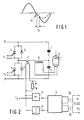
- the electronic switches are formed by thyristors, which are connected in the forward direction to the DC voltage source and each of which has a diode connected in anti-parallel. With such electronic switches, it is not possible to let the semi-oscillations flow one after the other through the push-pull switches, as can be seen in FIG. 1, which shows the time course of the resonant circuit current in the known inverter arrangement. It is assumed that a thyristor is conductive during the one positive half-oscillation. After the current has passed through zero, the diode connected in parallel with the thyristor initially takes over the ring-back current and the ignited thyristor loses its current Conductivity. As a result of the active power delivered to the consumer, the negative half-oscillation of the return oscillation current (indicated partly by dashed lines in FIG. 1) has a smaller amplitude than the positive half-oscillation.
- the push-pull controlled thyristor may only be fired if the so-called free time (tq), which is required for the removal of the charge carriers, has elapsed after the zero current has passed through the previously conductive thyristor.
- tq free time
- the ignition pulse can be generated with the aid of a delay circuit which is started by the current zero crossing.
- a comparator circuit is generally provided, the input of which is supplied with a value proportional to the instantaneous resonant circuit current and which responds as soon as the resonant circuit current has dropped below a value i s .
- This value i s must be large enough to prevent interference signals superimposed on the measurement signal from starting the delay circuit and thus possibly triggering the premature generation of the ignition pulses. Between the extinction of the one thyristor, at least a period of time must elapse that corresponds to the sum of the release time and the time within which the ringing current reaches the value i s after the current zero crossing. In the case of a particularly large load or a particularly large output of active power, it may even happen that the oscillation current does not reach the value i s , so that the ignition pulse starting the next half oscillation cannot be generated. This results in voltage or current drops in the load.
- the object of the present invention is to design an inverter of the type mentioned at the outset in such a way that the period within which the resonant circuit current passes from one electronic switch to the other can be shortened, so that the power which can be output is increased.
- GTO thyristors serve as electronic switches, which are connected by a pulse generator arrangement which generates a blocking pulse in the region of the zero crossing of the resonant circuit current and by means of which an ignition pulse for the subsequently conducting GTO thyristor after a defined delay time can be generated after the blocking pulse takes effect.
- GTO Gate Turn Off
- the invention takes advantage of the fact that in an inverter of the type mentioned at the outset, the current flowing through the electronic switching elements tends towards a zero crossing in a sinusoidal manner. In the area of the zero crossing of the resonant circuit current, however, the current-carrying GTO thyristor can operate with a relatively low-power lock impulses are blocked. A weak pulse generator is sufficient for this. As such, a GTO thyristor no longer conducts after the current through it has passed zero. However, the blocking pulse accelerates the charge carrier breakdown in the GTO thyristor and thus considerably shortens the release time. The ignition pulse for the next GTO thyristor can then follow the blocking pulse at the shortest possible time interval, so that there is hardly any gap between the two half-oscillations.
- the blocking pulse does not have to start exactly at the zero crossing of the resonant circuit current; it can also be a little earlier (up to 2% of the period), i.e. in the area of the zero crossing.
- the blocking pulses are delivered even further before the zero crossing by a relatively high-resistance pulse generator, they are practically short-circuited by the then very low-resistance gate-cathode path of the GTO thyristor. This only changes when the mentioned route becomes high-resistance. Although the blocking pulse starts relatively early in this case, it only becomes effective in the area of the zero crossing.
- a simpler embodiment of the invention provides that a measuring device for the resonant circuit current is provided, which is coupled to a comparator circuit which responds when the resonant circuit current falls below a reference value, and that the pulse generator arrangement is controlled by the comparator circuit in such a way that the blocking pulse is generated with a defined delay after falling below the reference value. It is therefore not necessary to measure the conductivity of the gate-cathode path of the GTO thyristors, but only the resonant circuit current, which must be measured anyway for control purposes.
- the time course of the active oscillation current half-wave - unlike the course of the return oscillation current - is largely independent of the load on the inverter.
- the timing of the blocking pulse and, subsequently, the timing of the ignition pulse for the other GTO thyristor - in each case based on the zero crossing of the resonant circuit current - do not depend on the load.
- a DC voltage is supplied to the inverter shown in FIG. 2, which can be generated from an AC voltage, for example by rectification (not shown in more detail).
- the series connection of two capacitors 1 and 2 of the same size is connected to the DC voltage, and the series connection of two electronic switches is connected in parallel.
- Each switch consists of a GTO thyristor 3 or 4 and a diode 5 or 6 connected antiparallel to it.
- connection points of the switches 3, 5 and 4,6 on the one hand and the capacitors 1,2 on the other hand are connected to one another via a bridge arm which comprises the series connection of the primary windings of a current transformer 7 for measuring the actual value of the resonant circuit current and a heating transformer 8, to the secondary winding of which the filament of an X-ray tube 9 is connected.
- the heating transformer is designed for the separation of the potentials on its primary side (almost earth potential) and its secondary side (negative high-voltage potential) and therefore has a relatively large leakage inductance, which together with the capacitors 1 and 2 has a series resonance circuit with a series resonance frequency of e.g. 15 kHz forms.
- a series resonance frequency e.g. 15 kHz forms.
- an oscillating circuit current flows through the capacitors 1 and 2, the primary winding 8 and the GTO thyristor 4, and in the other half oscillation a current flows through the GTO thyristor 3, the primary winding 8 and the capacitors 1 and 2.
- a resistor 10 is connected to the secondary winding of the current transformer 7.
- the voltage across this resistor is proportional to the instantaneous value of the current through the primary winding 8.
- the controller 11 compares the setpoint I o of the heating current with the effective value of the measured current (to generate this effective value from the instantaneous value at the resistor 10, an RMS module (not shown in more detail) must be available to generate the effective value be) and provides an output signal that depends on the difference between these values.
- the window comparator 12 responds as soon as the instantaneous value of the current has dropped below a value i s .
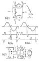
- the structure of this window comparator is shown in Fig. 3.
- the comparator comprises two amplifiers 121 and 122 with a high-resistance output, to which the voltage across the resistor 10 is supplied.
- the non-inverting inputs of the amplifiers 121 and 122 are connected to the tap of a voltage divider 123 connected between ground and the positive supply voltage V + or to the signal input of the comparator.
- the inverting inputs of the amplifiers 121 and 122 are connected to the signal input and the tap of a further voltage divider 124 connected between ground and the negative supply voltage V.
- the outputs of the two amplifiers 121, 122 are connected to one another and to the positive supply voltage V + via a resistor 125. These outputs also form the output of the window comparator.
- amplifier 121 receives a current (amplifier 122 is blocked) so that the common output has a low potential. If the voltage at the common input falls below the voltage at the tap of the potentiometer 123 (in this case the resonant circuit current has dropped below the value i s ), then the amplifier 121 also no longer delivers current. Only after the common input voltage has fallen below a negative value that corresponds to the voltage at the tap of the potentiometer 124, the amplifier 122 supplies a current. The window comparator thus delivers a positive pulse at each zero crossing of the resonant circuit current (in both directions), the leading edge of which is used to generate a blocking pulse.
- the controller 11 and the window comparator 12 control a trigger circuit 13 which, similar to the trigger circuits for thyristors and others.
- the blocking pulses begin after a defined delay time after the leading edge of the pulses supplied by the window comparator 12.
- the trigger circuit has two outputs, which are coupled via pulse transmitters 14 and 15 to the gate-cathode sections of the GTO thyristors 3 and 4, respectively.
- the first (positive) half oscillation of the resonant circuit current Mes is initiated by an ignition pulse for the associated GTO thyristor (eg 3) (voltage u 1) after the other GTO thyristor (4) has been blocked.
- the firing pulse must last at least as long that the resonant circuit current has exceeded the value of the latching current before the firing pulse ends. After the half oscillation has passed its maximum (e.g.
- the window comparator delivers a positive pulse, which within the trigger circuit causes a blocking pulse to be generated which has the opposite polarity to the previous ignition pulse , and whose leading edge is offset from the leading edge of the pulse supplied by the window comparator 12 by a defined delay time t d .
- t d 0.6 microseconds at the specified value i s is a favorable value which results from the delay times of the trigger circuit 13 and the pulse transmitter 14, 15 - that is to say without an additional delay element.
- the blocking pulse is timed so that it does not terminate the half-oscillation prematurely, but on the other hand the charge carriers are removed from the blocked GTO thyristor as soon as possible after the zero crossing of the resonant circuit current.
- the GTO thyristor 4 After blocking the thyristor 3, the GTO thyristor 4 is ignited (with u2). A period must elapse between the leading edges of the blocking pulse for the GTO thyristor 3 and the ignition pulse for the GTO thyristor 4, which corresponds at least to the greatest possible release time t q . With a suitable adaptation between the threshold values i s , t d and t q it can be achieved that the subsequent negative half-oscillation together with the previous positive half-oscillation results in an almost sinusoidal current curve.
- a blocking pulse for the GTO thyristor 4 follows, followed by an ignition pulse for the GTO thyristor 3 again with the delay time mentioned.
- the blocking pulses can be made so wide that they overlap with the ignition pulses, as long as it is ensured that the required delay (t q ) exists between the blocking pulse for one GTO thyristor and the ignition pulse for the other GTO thyristor.
- FIGS. 4a and 4b show that the blocking pulses are always generated - with a delay - regardless of the output power, when the amount of the current drops below the value i s .
- an ignition pulse can be generated for the other GTO thyristor (as in FIG. 4a), but this pulse can also be generated later, as in FIG. 4b.
- the inverter comprises two switching branches connected in parallel to the supply voltage terminals + and -, each of which consists of the series connection of two electronic switching elements 21 and 22 or 23 and 24.
- Each of these electronic switching elements consists of a GTO thyristor and an anti-parallel diode.
- the series connection of a capacitor 25 and the primary winding 26 of a high-voltage transformer 27 is connected between the connection points of the switching elements 21 and 22 on the one hand and the switching elements 23 and 24 on the other hand. This has a relatively large leakage inductance which, together with the capacitor 25, forms a series resonance circuit.
- the high-voltage transformer 27 has two secondary windings 28 and 29, respectively, which feed a rectifier 30 and 31, respectively, for generating a positive or negative high voltage, which is smoothed by capacitors 32 and 33 and which is supplied to the anode or the cathode of the X-ray tube 9.
- the switching elements 21 and 24 located in the bridge diagonal are each supplied with the same pulse voltage, if one disregards the required potential offset.
- the resonant circuit current flows through elements 25, 26, i.e. via switches 21 and 24, and in the other half oscillation, via switches 22 and 23.
- the series resonant inverter delivers its maximum power when the GTO thyristors in the electronic Switches are blocked shortly before reaching zero crossing and after the shortened release time the GTO thyristors located in the respective other current path are ignited.
Abstract
Description
Die Erfindung betrifft eine Wechselrichteranordnung, insbesondere für einen Röntgengenerator, mit einem Serien-Schwingkreis und wenigstens zwei von je einer Halbschwingung des Schwingkreisstromes durchflossenen, im Gegentakt geschalteten elektronischen Schaltern, über die der Serien-Schwingkreis mit einer Gleichspannungsquelle koppelbar ist.The invention relates to an inverter arrangement, in particular for an X-ray generator, with a series oscillating circuit and at least two electronic switches through which a half oscillation of the oscillating circuit current flows and which are switched in push-pull manner and via which the series oscillating circuit can be coupled to a DC voltage source.
Derartige Wechselrichter sind bekannt (DE-OS 3046 413; DE-OS 30 46 767 und DE-OS 32 18 535). Die elektronischen Schalter sind dabei während jeweils einer Halbschwingung leitend, und die von einem derartigen Wechselrichter erzeugbare elektrische Leistung ist umso größer, je dichter die Halbschwingungen aufeinander folgen, die im Gegentakt die elektronischen Schalter durchfließen.Such inverters are known (DE-OS 3046 413; DE-OS 30 46 767 and DE-OS 32 18 535). The electronic switches are each conductive during one half-oscillation, and the electrical power that can be generated by such an inverter is greater the closer the half-oscillations follow one another, which flow through the electronic switches in push-pull.
Bei den bekannten Wechselrichtern werden die elektronischen Schalter durch Thyristoren gebildet, die in Durchlaßrichtung mit der Gleichspannungsquelle verbunden sind und denen jeweils eine Diode antiparallel geschaltet ist. Bei derartigen elektronischen Schaltern ist es nicht möglich, die Halbschwingungen unmittelbar nacheinander durch die in Gegentakt gesteuerten Schalter fließen zu lassen, wie sich aus Fig. 1 ergibt, die den zeitlichen Verlauf des Schwingkreisstroms bei der bekannten Wechselrichteranordnung darstellt. Dabei ist angenommen, daß während der einen positiven Halbschwingung ein Thyristor leitend ist. Nach dem Stromnulldurchgang übernimmt die dem Thyristor parallelgeschaltete Diode zunächst den Rückschwingstrom und der gezündete Thyristor verliert seine Leitfähigkeit. Die negative Halbschwingung des Rückschwingstroms (in Fig. 1 zum Teil gestrichelt angedeutet) hat als Folge der an den Verbraucher abgegebenen Wirkleistung eine kleinere Amplitude als die positive Halbschwingung.In the known inverters, the electronic switches are formed by thyristors, which are connected in the forward direction to the DC voltage source and each of which has a diode connected in anti-parallel. With such electronic switches, it is not possible to let the semi-oscillations flow one after the other through the push-pull switches, as can be seen in FIG. 1, which shows the time course of the resonant circuit current in the known inverter arrangement. It is assumed that a thyristor is conductive during the one positive half-oscillation. After the current has passed through zero, the diode connected in parallel with the thyristor initially takes over the ring-back current and the ignited thyristor loses its current Conductivity. As a result of the active power delivered to the consumer, the negative half-oscillation of the return oscillation current (indicated partly by dashed lines in FIG. 1) has a smaller amplitude than the positive half-oscillation.
Der im Gegentakt gesteuerte Thyristor darf erst gezündet werden, wenn nach dem Stromnulldurchgang durch den vorher leitenden Thyristor die sogenannte Freiwerdezeit (tq) verstrichen ist, die für den Abbau der Ladungsträger benötigt wird. Wie in der DE-OS 30 46767 beschrieben, kann der Zündimpuls mit Hilfe einer Verzögerungsschaltung erzeugt werden, die durch den Stromnulldurchgang gestartet wird. Zur Erkennung des Stromnulldurchganges ist in der Regel eine Komparatorschaltung vorgesehen, deren Eingang ein dem momentanen Schwingkreisstrom proportionaler Wert zugeführt wird und die anspricht, sobald der Schwingkreisstrom unter einen Wert is gesunken ist. Dieser Wert is muß genügend groß sein, um zu verhindern, daß dem Meßsignal überlagerte Störsignale die Verzögerungsschaltung starten und damit unter Umständen ein vorzeitiges Erzeugen der Zündimpulse auslösen können. Zwischen dem Erlöschen des einen Thyristors muß also zumindest ein Zeitraum verstreichen, der der Summe aus der Freiwerdezeit und der Zeit entspricht, innerhalb der der Rückschwingstrom nach dem Stromnulldurchgang den Wert is erreicht. Bei einer besonders großen Last bzw. einer besonders großen abgegebenen Wirkleistung kann es dabei sogar vorkommen, daß der Rückschwingstrom den Wert is nicht erreicht, so daß der die nächste Halbschwingung startende Zündimpuls nicht erzeugt werden kann. Daraus resultieren Spannungs- bzw. Stromeinbrüche an der Last.The push-pull controlled thyristor may only be fired if the so-called free time (tq), which is required for the removal of the charge carriers, has elapsed after the zero current has passed through the previously conductive thyristor. As described in DE-OS 30 46767, the ignition pulse can be generated with the aid of a delay circuit which is started by the current zero crossing. To detect the current zero crossing, a comparator circuit is generally provided, the input of which is supplied with a value proportional to the instantaneous resonant circuit current and which responds as soon as the resonant circuit current has dropped below a value i s . This value i s must be large enough to prevent interference signals superimposed on the measurement signal from starting the delay circuit and thus possibly triggering the premature generation of the ignition pulses. Between the extinction of the one thyristor, at least a period of time must elapse that corresponds to the sum of the release time and the time within which the ringing current reaches the value i s after the current zero crossing. In the case of a particularly large load or a particularly large output of active power, it may even happen that the oscillation current does not reach the value i s , so that the ignition pulse starting the next half oscillation cannot be generated. This results in voltage or current drops in the load.
Aufgabe der vorliegenden Erfindung ist es, einen Wechselrichter der eingangs genannten Art so auszugestalten, daß der Zeitraum, innerhalb dessen der Schwingkreisstrom vom einen elektronischen Schalter auf den anderen übergeht, verkürzt werden kann, so daß die abgebbare Leistung vergrößert wird.The object of the present invention is to design an inverter of the type mentioned at the outset in such a way that the period within which the resonant circuit current passes from one electronic switch to the other can be shortened, so that the power which can be output is increased.
Diese Aufgabe wird erfindungsgemäß dadurch gelöst, daß als elektronische Schalter GTO-Thyristoren dienen, die von einer Impulserzeugeranordnung geschaltet sind, welche im Bereich des Nulldurchganges des Schwingkreisstroms jeweils einen Sperrimpuls erzeugt und durch welche ein Zündimpuls für den anschließend leitenden GTO-Thyristor nach einer definierten Verzögerungszeit nach dem Wirksamwerden des Sperrimpulses erzeugbar ist.This object is achieved in that GTO thyristors serve as electronic switches, which are connected by a pulse generator arrangement which generates a blocking pulse in the region of the zero crossing of the resonant circuit current and by means of which an ignition pulse for the subsequently conducting GTO thyristor after a defined delay time can be generated after the blocking pulse takes effect.
Die Erfindung verwendet also GTO-Thyristoren (GTO=Gate Turn Off). Es ist bekannt, daß GTO-Thyristoren wie normale Thyristoren betrieben werden können, falls ihrem Gate nur Zündimpulse zugeführt werden. In diesem Fall wird auch der GTO-Thyristor erst nach dem Stromnulldurchgang gesperrt. Es ist aber auch möglich, durch einen Sperrimpuls, der die entgegengesetzte Polarität haben muß wie der Zündimpuls, einen GTO-Thyristor zu sperren, bevor der ihn durchfließende Strom durch Null geht. Von dieser Möglichkeit wird bei dem in der EP-OS137 401 beschriebenen Wechselrichter Gebrauch gemacht. Über das Gate des Thyristors müssen in diesem Fall mindestens 20% des zu schaltenden Stromes als Sperrstrom fließen, was einen entsrechend leistungsstarken und daher teuren Impulserzeuger voraussetzt.The invention therefore uses GTO thyristors (GTO = Gate Turn Off). It is known that GTO thyristors can be operated like normal thyristors if only ignition pulses are supplied to their gate. In this case, the GTO thyristor is also blocked only after the current zero crossing. However, it is also possible to block a GTO thyristor by means of a blocking pulse, which must have the opposite polarity as the ignition pulse, before the current flowing through it passes through zero. This option is used in the inverter described in EP-OS137 401. In this case, at least 20% of the current to be switched must flow as reverse current via the gate of the thyristor, which requires a correspondingly powerful and therefore expensive pulse generator.
Die Erfindung nutzt die Tatsache aus, daß bei einem Wechselrichter der eingangs genannten Art der die elektronischen Schaltelemente durchfließende Strom sinusförmig einem Nulldurchgang zustrebt. Im Bereich des Nulldurchganges des Schwingkreisstromes kann der stromführende GTO-Thyristor aber mit relativ leistungsschwachen Sperr impulsen gesperrt werden. Dafür reicht ein leistungsschwacher Impulserzeuger aus. An sich leitet ein GTO-Thyristor nach dem Nulldurchgang des ihn durchfließenden Stromes ohnehin nicht mehr. Durch den Sperrimpuls wird aber der Ladungsträgerabbau in dem GTO-Thyristor beschleunigt und damit die Freiwerdezeit erheblich verkürzt. Der Zündimpuls für den nächsten GTO-Thyristor kann dann dem Sperrimpuls in kürzestem zeitlichen Abstand folgen, so daß sich zwischen den beiden Halbschschwingungen kaum noch eine Lücke ergibt.The invention takes advantage of the fact that in an inverter of the type mentioned at the outset, the current flowing through the electronic switching elements tends towards a zero crossing in a sinusoidal manner. In the area of the zero crossing of the resonant circuit current, however, the current-carrying GTO thyristor can operate with a relatively low-power lock impulses are blocked. A weak pulse generator is sufficient for this. As such, a GTO thyristor no longer conducts after the current through it has passed zero. However, the blocking pulse accelerates the charge carrier breakdown in the GTO thyristor and thus considerably shortens the release time. The ignition pulse for the next GTO thyristor can then follow the blocking pulse at the shortest possible time interval, so that there is hardly any gap between the two half-oscillations.
Der Sperrimpuls muß nicht exakt im Nulldurchgang des Schwingkreisstromes beginnen; er kann auch etwas (bis zu 2% der Periodendauer) früher oder später, d.h. im Bereich des Nulldurchgangs, erzeugt werden.The blocking pulse does not have to start exactly at the zero crossing of the resonant circuit current; it can also be a little earlier (up to 2% of the period), i.e. in the area of the zero crossing.
Wenn die Sperrimpulse noch weiter vor dem Nulldurchgang von einem relativ hochohmigen Impulserzeuger geliefert werden, werden sie durch die dann noch sehr niederohmige Gate-Kathoden-Strecke des GTO-Thyristors praktisch kurzgeschlossen. Dies ändert sich erst, wenn die genannte Strecke hochohmiger wird. Obwohl in diesem Fall der Sperrimpuls schon relativ früh beginnt, wird er erst im Bereich des Nulldurchgangs wirksam.If the blocking pulses are delivered even further before the zero crossing by a relatively high-resistance pulse generator, they are practically short-circuited by the then very low-resistance gate-cathode path of the GTO thyristor. This only changes when the mentioned route becomes high-resistance. Although the blocking pulse starts relatively early in this case, it only becomes effective in the area of the zero crossing.
Wie sich aus obigem ergibt, besteht eine Möglichkeit für die Festlegung des Anfangs eines Sperrimpulses darin, die Leitfähigkeit der Gate-Kathoden-Strecke zu bestimmen. Dies ist jedoch verhältnismäßig aufwendig, weil es die Messung der Leitfähigkeit dieser Strecke erfordert. Eine einfachere Ausgestaltung der Erfindung sieht demgegenüber vor, daß eine Meßeinrichtung für den Schwingkreisstrom vorgesehen ist, die mit einer Komparatorschaltung gekoppelt ist, die anspricht, wenn der Schwingkreisstrom einen Referenzwert unterschreitet, und daß die Impulserzeugeranordnung von der Komparatorschaltung gesteuert wird, derart, daß der Sperrimpuls mit definierter Verzögerung nach dem Unterschreiten des Referenzwertes erzeugt wird. Hierbei muß also nicht die Leitfähigkeit der Gate-Kathoden-Strecke der GTO-Thyristoren gemessen werden, sondern nur der Schwingkreisstrom, der zu Regelzwecken ohnehin gemessen werden muß. Der zeitliche Verlauf der aktiven Schwingstromhalbwelle ist - anders als der Verlauf des Rückschwingstromes - von der Belastung des Wechselrichters weitgehend unabhängig. Infolgedessen hängt die zeitliche Lage des Sperrimpulses und in seiner Folge die zeitliche Lage des Zündimpulses für den anderen GTO-Thyristor - jeweils bezogen auf den Nulldurchgang des Schwingkreisstromes - nicht von der Belastung ab. Insbesondere kann es nicht zum Ausfall eines Zündimpulses kommen - wie bei Wechselrichtern der eingangs genannten Art.As can be seen from the above, one possibility for determining the start of a blocking pulse is to determine the conductivity of the gate-cathode path. However, this is relatively expensive because it requires measuring the conductivity of this route. In contrast, a simpler embodiment of the invention provides that a measuring device for the resonant circuit current is provided, which is coupled to a comparator circuit which responds when the resonant circuit current falls below a reference value, and that the pulse generator arrangement is controlled by the comparator circuit in such a way that the blocking pulse is generated with a defined delay after falling below the reference value. It is therefore not necessary to measure the conductivity of the gate-cathode path of the GTO thyristors, but only the resonant circuit current, which must be measured anyway for control purposes. The time course of the active oscillation current half-wave - unlike the course of the return oscillation current - is largely independent of the load on the inverter. As a result, the timing of the blocking pulse and, subsequently, the timing of the ignition pulse for the other GTO thyristor - in each case based on the zero crossing of the resonant circuit current - do not depend on the load. In particular, there can be no failure of an ignition pulse - as with inverters of the type mentioned at the beginning.
Die Erfindung wird nachstehend anhand der Zeichnung näher erläutert. Es zeigen
- Fig. 1 den zeitlichen Verlauf des Schwingkreisstroms bei einem Serienresonanz-Wechselrichter, dessen elektronische Schalter jeweils einen Thyristor umfassen,
- Fig. 2 einen erfindungsgemäßen Wechselrichter zur Erzeugung des Heizstromes einer Röntgenröhre,
- Fig. 3 einen dabei verwendbaren Fenster-Komparator,
- Fig. 4a und 4b den zeitlichen Verlauf verschiedener Signale bei maximaler und bei verminderter abgegebener Leistung und
- Fig. 5 ein Prinzipschaltbild eines für die Hochspannungserzeugung einer Röntgenröhre benutzten Wechselrichters, bei dem die Erfindung ebenfalls anwendbar ist.
- 1 shows the time course of the resonant circuit current in a series resonance inverter, the electronic switches of which each comprise a thyristor,
- 2 shows an inverter according to the invention for generating the heating current of an X-ray tube,
- 3 shows a window comparator that can be used,
- 4a and 4b the time course of various signals at maximum and with reduced output and
- Fig. 5 is a schematic diagram of an inverter used for high voltage generation of an X-ray tube, in which the invention can also be used.
An den Eingangsklemmen + und - wird dem in Fig. 2 gezeigten Wechselrichter eine Gleichspannung zugeführt, die beispielsweise durch Gleichrichtung (nicht näher dargestellt) aus einer Wechselspannung erzeugt werden kann. An die Gleichspannung ist die Serienschaltung zweier gleich großer Kondensatoren 1 und 2 angeschlossen, der die Serienschaltung zweier elektronischer Schalter parallelgeschaltet ist. Jeder Schalter besteht aus einem GTO-Thyristor 3 bzw. 4 und einer dazu antiparallel geschalteten Diode 5 bzw. 6. Die Verbindungspunkte der Schalter 3, 5 und 4,6 einerseits sowie der Kondensatoren 1,2 andererseits sind über einen Brückenzweig miteinander verbunden, der die Serienschaltung der Primärwicklungen eines Stromwandlers 7 zur Messung des Istwertes des Schwingkreisstroms und eines Heiztransformators 8 umfaßt, an dessen Sekundärwicklung der Heizfaden einer Röntgenröhre 9 angeschlossen ist.At the input terminals + and -, a DC voltage is supplied to the inverter shown in FIG. 2, which can be generated from an AC voltage, for example by rectification (not shown in more detail). The series connection of two
Der Heiztransformator ist für die Trennung der Potentiale auf seiner Primärseite (nahezu Erdpotential) und seiner Sekundärseite (negatives Hochspannungspotential) ausgelegt und besitzt daher eine relativ große Streuinduktivität, die zusammen mit einem den Kondensatoren 1 und 2 einen Serienresonanzkreis mit einer Serienresonanzfrequenz von z.B. 15 kHz bildet. Bei der einen Halbschwingung fließt ein Schwingkreisstrom über die Kondensatoren 1 und 2, die Primärwicklung 8 und den GTO-Thyristor 4, und bei der anderen Halbschwingung fließt ein Strom über den GTO-Thyristor 3, die Primärwicklung 8 und die Kondensatoren 1 und 2.The heating transformer is designed for the separation of the potentials on its primary side (almost earth potential) and its secondary side (negative high-voltage potential) and therefore has a relatively large leakage inductance, which together with the
An die Sekundärwicklung des Stromwandlers 7 ist ein Widerstand 10 angeschlossen. Die Spannung an diesem Widerstand ist dem Momentanwert des Stromes durch die Primärwicklung 8 proportional. Sie wird einerseits einem Regler 11 mit PI-Charakteristik zugeführt und andererseits einem Fensterkomparator 12. Der Regler 11 vergleicht den Sollwert Io des Heizstroms mit dem Effektivwert des gemessenen Stroms (zur Erzeugung dieses Effektivwertes aus dem Momentanwert am Widerstand 10 muß ein nicht näher dargestellter RMS-Baustein zur Erzeugung des Effektivwertes vorhanden sein) und liefert ein Ausgangssignal, das von der Differenz dieser Werte abhängt. Der Fensterkomparator 12 spricht an, sobald der Momentanwert des Stromes unter einen Wert is gesunken ist. Dieser Wert soll zwar klein im Vergleich zur Amplitude des Schwingkreisstromes sein, aber immer noch so groß, daß das Ansprechen weitgehend unbeeinflußt von Störsignalen erfolgt; bei einer Amplitude von 8A beispielsweise ist is=0,5A ein geeigneter Wert. Der Aufbau dieses Fensterkomparators ist in Fig. 3 dargestellt.A
Der Komparator umfaßt zwei Verstärker 121 und 122 mit hochohmigem Ausgang, denen die Spannung am Widerstand 10 zugeführt wird. Die nichtinvertierenden Eingänge der Verstärker 121 bzw. 122 sind mit dem Abgriff eines zwischen Masse und die positive Versorgungsspannung V+geschalteten Spannungsteilers 123 bzw. mit dem Signaleingang des Komparators verbunden. Die invertierenden Eingänge der Verstärker 121 bzw. 122 sind mit dem Signaleingang bzw. dem Abgriff eines weiteren, zwischen Masse und die negative Versorgungsspannung V-geschalteten Spannungsteilers 124 verbunden. Die Ausgänge der beiden Verstärker 121, 122 sind miteinander sowie über einen Widerstand 125 mit der positiven Versorgungsspannung V+verbunden. Diese Ausgänge bilden auch den Ausgang des Fensterkomparators.The comparator comprises two
Solange der Schwingkreisstrom positiv ist und mithin die Spannung am Widerstand 10 größer ist als die positive Gleichspannung am Abgriff des Potentiometers 123, liefert der Verstärker 121 einen Strom (der Verstärker 122 ist gesperrt), so daß sich am gemeinsamen Ausgang ein niedriges Potential ergibt. Sinkt die Spannung am gemeinsamen Eingang unter die Spannung am Abgriff des Potentiometers 123 (in diesem Fall ist der Schwingkreistrom unter den Wert is gesunken), dann liefert auch der Verstärker 121 keinen Strom mehr. Erst nachdem die gemeinsame Eingangsspannung einen negativen Wert unterschritten hat, der der Spannung am Abgriff des Potentiometers 124 entspricht, liefert der Verstärker 122 einen Strom. Somit liefert der Fensterkomparator bei jedem Nulldurchgang des Schwingkreisstroms (in beiden Richtungen) einen positiven Impuls, dessen Vorderflanke zur Erzeugung eines Sperrimpulses dient.As long as the resonant circuit current is positive and therefore the voltage across
Der Regler 11 und der Fensterkomparator 12 steuern eine Triggerschaltung 13, die ähnlich den Triggerschaltungen für Thyristoren u.a. Flip-Flops, logische Verknüpfungsschaltungen und einen spannungsgesteuerten Oszillator enthalten kann, der von dem Regler 11 gesteuert wird und die Frequenz der Zündimpulse bestimmt. Die Sperrimpulse beginnen nach einer definierten Verzögerungszeit nach der Vorderflanke der von dem Fensterkomparator 12 gelieferten Impulse. Die Triggerschaltung besitzt zwei Ausgänge, die über Impulsübertrager 14 bzw. 15 mit den Gate-Kathoden-Strecken der GTO-Thyristoren 3 bzw. 4 gekoppelt sind.The
Die Arbeitsweise der Triggerschaltung ergibt sich aus den Figuren 4a und 4b, die den zeitlichen Verlauf des Schwingkreisstromes (1. Zeile) und der Ausgangsspannungen der Impulsübertrager u₁ bzw. u₂ (2. und 3. Zeile) für maximale Ausgangsleistung (Fig. 4a) und für eine niedrigere Ausgangsleistung (Fig. 4b) darstellen.The operation of the trigger circuit results from Figures 4a and 4b, the time course of the resonant circuit current (1st line) and the output voltages of the pulse transmitters u₁ and u₂ (2nd and 3rd line) for maximum output power (Fig. 4a) and represent for a lower output power (Fig. 4b).
Die erste (positive) Halbschwingung des Schwingkreisstro mes wird durch einen Zündimpuls für den zugehörigen GTO-Thyristor (z.B. 3) eingeleitet (Spannung u₁), nachdem zuvor der andere GTO-Thyristor (4) gesperrt worden ist. Der Zündimpuls muß mindestens solange dauern, daß der Schwingkreisstrom den Wert des Einraststroms überschritten hat, bevor der Zündimpuls endet. Nachdem die Halbschwingung ihr Maximum (z.B. 8A) durchlaufen und der Schwingkreisstrom schließlich einen Wert is (z.B.) unterschritten hat, liefert der Fensterkomparator einen positiven Impuls, der innerhalb der Triggerschaltung die Erzeugung eines Sperrimpulses bewirkt, der die entgegengesetzte Polarität hat wie der vorherige Zündimpuls, und dessen Vorderflanke gegenüber der Vorderflanke des von dem Fensterkomparator 12 gelieferten Impulses um eine definierte Verzögerungszeit td versetzt ist. Bei einer Dauer der Halbschwingung von z.B. 33 µs ist td=0,6µs bei dem angegebenen Wert is ein günstiger Wert, der sich aus den Verzögerungszeiten der Triggerschaltung 13 und der Impulsübertrager 14,15 ergibt - also ohne zusätzliches Verzögerungsglied. Der Sperrimpuls liegt im günstigsten Falle zeitlich so, daß die Halbschwingung durch ihn nicht vorzeitig beendet wird, andererseits die Ladungsträger aus dem gesperrten GTO-Thyristor aber möglichst unmittelbar nach dem Nulldurchgang des Schwingkreisstromes beseitigt sind.The first (positive) half oscillation of the resonant circuit current Mes is initiated by an ignition pulse for the associated GTO thyristor (eg 3) (voltage u 1) after the other GTO thyristor (4) has been blocked. The firing pulse must last at least as long that the resonant circuit current has exceeded the value of the latching current before the firing pulse ends. After the half oscillation has passed its maximum (e.g. 8A) and the resonant circuit current has finally fallen below a value i s (e.g.), the window comparator delivers a positive pulse, which within the trigger circuit causes a blocking pulse to be generated which has the opposite polarity to the previous ignition pulse , and whose leading edge is offset from the leading edge of the pulse supplied by the
Nach dem Sperren des Thyristors 3 wird der GTO-Thyristor 4 gezündet( mit u₂). Zwischen den Vorderflanken des Sperrimpulses für den GTO-Thyristor 3 und des Zündimpulses für den GTO-Thyristor 4 muß dabei ein Zeitraum verstreichen, der zumindest der größtmöglichen Freiwerdezeit tq entspricht. Bei geeigneter Anpassung zwischen dem Schwellenwert is,td und tq läßt sich erreichen, daß die sich anschließende negative Halbschwingung zusammen mit der vorigen positiven Halbschwingung einen nahezu sinusförmigen Stromverlauf ergibt. Wenn nach dem Zünden des GTO-Thyristors die negative Halbschwingung den Wert -is erreicht hat, folgt ein Sperrimpuls für den GTO-Thyristor 4, wonach mit der erwähnten Verzögerungszeit wiederum ein Zündimpuls für den GTO-Thyristor 3 folgt. Die Sperrimpulse können so breit gemacht werden, daß sie sich mit den Zündimpulsen überlappen, solange sichergestellt ist, daß zwischen dem Sperrimpuls für den einen GTO-Thyristor und den Zündimpuls für den anderen GTO-Thyristor die erforderliche Verzögerung (tq) besteht.After blocking the thyristor 3, the GTO thyristor 4 is ignited (with u₂). A period must elapse between the leading edges of the blocking pulse for the GTO thyristor 3 and the ignition pulse for the GTO thyristor 4, which corresponds at least to the greatest possible release time t q . With a suitable adaptation between the threshold values i s , t d and t q it can be achieved that the subsequent negative half-oscillation together with the previous positive half-oscillation results in an almost sinusoidal current curve. If after igniting the GTO thyristor the negative half-oscillation has reached the value -i s , a blocking pulse for the GTO thyristor 4 follows, followed by an ignition pulse for the GTO thyristor 3 again with the delay time mentioned. The blocking pulses can be made so wide that they overlap with the ignition pulses, as long as it is ensured that the required delay (t q ) exists between the blocking pulse for one GTO thyristor and the ignition pulse for the other GTO thyristor.
Fig. 4b zeigt die gleichen Signale bei einer geringeren vom Wechselrichter abgegebenen Leistung. Dabei ist angenommen, daß die erste Stromhalbschwingung noch im Nulldurchgang gezündet worden ist. Wenn der Maximalwert überschritten und wiederum der Wert is erreicht ist, wird wiederum ein Sperrimpuls für den Thyristor 3 erzeugt. Der Zündimpuls für den GTO-Thyristor 4 folgt aber nicht schon nach Ablauf der Freiwerdezeit, sondern wesentlich später. Zwischen dem Nulldurchgang der positiven Halbschwingung und dem Zündimpuls für den Thyristor 4 ergibt sich daher zunächst ein negativer Rückschwingstrom, der über die Diode 5 fließt. Erst nach dem Zündimpuls für den Thyristor 4 endet diese Phase, der dann ein Teil der negativen Halbschwingung folgt.4b shows the same signals with a lower power output by the inverter. It is assumed that the first current half-wave was still ignited at the zero crossing. If the maximum value is exceeded and the value i s is reached again, a blocking pulse for the thyristor 3 is generated. The firing pulse for the GTO thyristor 4 does not follow after the expiration time, but much later. Between the zero crossing of the positive half-oscillation and the firing pulse for the thyristor 4, there is therefore initially a negative ring-back current which flows via the diode 5. This phase only ends after the firing pulse for thyristor 4, which then follows part of the negative half-oscillation.
Der Vergleich der Figuren 4a und 4b zeigt, daß die Sperrimpulse unabhängig von der abgegebenen Leistung immer dann - mit Verzögerung - erzeugt werden, wenn der Strom dem Betrage nach unter den Wert is sinkt. Nach Ablauf der Freiwerdezeit tg kann ein Zündimpuls für den jeweils anderen GTO-Thyristor erzeugt werden (wie in Fig. 4a), doch kann dieser Impuls auch später erzeugt werden, wie in Fig. 4b.The comparison of FIGS. 4a and 4b shows that the blocking pulses are always generated - with a delay - regardless of the output power, when the amount of the current drops below the value i s . After the release time tg has elapsed, an ignition pulse can be generated for the other GTO thyristor (as in FIG. 4a), but this pulse can also be generated later, as in FIG. 4b.
In Fig. 5 ist ein Serienresonanz-Wechselrichter für die Erzeugung der Hochspannung für eine Röntgenröhre 9 dargestellt, der ebenfalls entsprechend der Erfindung aufgebaut sein kann. Hierbei umfaßt der Wechselrichter jeweils zwei parallel an die Versorgungsspannungsklemmen + und - angeschlossene Schaltzweige, die aus der Serienschaltung jeweils zweier elektronischer Schaltelemente 21 und 22 bzw. 23 und 24 bestehen. Jedes dieser elektronischen Schaltelemente besteht aus einem GTO-Thyristor und einer dazu antiparallel geschalteten Diode. Zwischen die Verbindungspunkte der Schaltelemente 21 und 22 einerseits und der Schaltelemente 23 und 24 anderseits ist die Serienschaltung eines Kondensators 25 und der Primärwicklung 26 eines Hochspannungstransformators 27 geschaltet. Dieser hat eine relativ große Streuinduktivität, die zusammen mit dem Kondensator 25 einen Serienresonanzkreis bildet. Der Hochspannungstransformator 27 hat zwei Sekundärwicklungen 28 bzw. 29, die einen Gleichrichter 30 bzw. 31 zur Erzeugung einer positiven bzw. negativen Hochspannung speisen, die von Kondensatoren 32 und 33 geglättet und der Anode bzw. der Kathode der Röntgenröhre 9 zugeführt wird.5 is a series resonance inverter for the Generation of the high voltage for an
Den in der Brückendiagonale befindlichen Schaltelementen 21 und 24 (bzw. 22 und 23) wird jeweils die gleiche Impulsspannung zugeführt, wenn man einmal von dem erforderlichen Potentialversatz absieht. Bei der einen Halbschwingung fließt der Schwingkreisstrom durch die Elemente 25, 26 also über die Schalter 21 und 24 und bei der anderen Halbschwingung über die Schalter 22 und 23. Auch in diesem Fall liefert der Serienresonanzwechselrichter seine Maximalleistung, wenn die GTO-Thyristoren in den elektronischen Schaltern kurz vor Erreichen des Nulldurchganges gesperrt werden und nach Ablauf der verkürzten Freiwerdezeit die im jeweils anderen Strompfad befindlichen GTO-Thyristoren gezündet werden.The switching
Claims (5)
dadurch ekennzeichnet, daß als elektronische Schalter GTO-Thyristoren (3,4) dienen, die von einer Impulserzeugeranordnung (13) geschaltet sind, welche im Bereich des Nulldurchganges des Schwingkreisstroms jeweils einen Sperrimpuls erzeugt und durch welche ein Zündimpuls für den anschließend leitenden GTO-Thyristor (z.B. 4) nach einer definierten Verzögerungszeit (tq) nach dem Wirksamwerden des Sperrimpulses erzeugbar ist.1. Inverter arrangement, in particular for an X-ray generator, with a series oscillating circuit and at least two electronic switches through which a half oscillation of the oscillating circuit current flows and which are switched in push-pull manner and via which the series oscillating circuit can be coupled to a direct voltage source,
characterized in that the electronic switches used are GTO thyristors (3, 4) which are connected by a pulse generator arrangement (13) which generates a blocking pulse in the region of the zero crossing of the resonant circuit current and through which an ignition pulse for the subsequently conducting GTO thyristor (eg 4) can be generated after a defined delay time (tq) after the blocking pulse takes effect.
dadurch gekennzeichnet, daß eine Meßeinrichtung (7,10) für den Schwingkreisstrom vorgesehen ist, die mit einer Komparatorschaltung gekoppelt (12) ist, die anspricht, wenn der Schwingkreisstrom einen Referenzwert (is) unterschreitet, und daß die Impulserzeugeranordnung von der Komparatorschaltung gesteuert wird, derart, daß der Sperrimpuls mit definierter Verzögerung (td) nach dem Unterschreiten des Referenzwertes erzeugt wird.2. Inverter arrangement according to claim 1,
characterized in that a measuring device (7, 10) for the oscillating circuit current is provided, which is coupled (12) to a comparator circuit which responds when the oscillating circuit current falls below a reference value (i s ), and in that the pulse generator arrangement is controlled by the comparator circuit , in such a way that the blocking pulse is generated with a defined delay (t d ) after falling below the reference value.
dadurch gekennzeichnet, daß die Komparatorschaltung ein Fensterkomparator (12) ist, dessen Ausgangssignal innerhalb eines zum Nullpunkt des Schwingkreisstromes symmetrischen Bereichs einen ersten Zustand und beiderseits dieses Bereichs einen zweiten Zustand einnimmt.3. Inverter arrangement according to claim 2,
characterized in that the comparator circuit is a window comparator (12), the output signal of which is within a range symmetrical to the zero point of the resonant circuit current and on both sides this area assumes a second state.
dadurch gekennzeichnet, daß die Induktivität des Schwingkreises durch die Primärwicklung eines Transformators (8) gebildet wird, dessen Sekundärwicklung mit dem Heizkreis einer Röntgenröhre (9) gekoppelt ist (Fig. 2).4. Inverter arrangement according to one of claims 1 to 3,
characterized in that the inductance of the resonant circuit is formed by the primary winding of a transformer (8), the secondary winding of which is coupled to the heating circuit of an X-ray tube (9) (Fig. 2).
dadurch ekennzeichnet, daß die Induktivität des Schwingkreises durch die Primärwicklung eines Transformators (27) gebildet wird, dessen Sekundärwicklungen (28,29) mit einem Hochspannungsgleichrichter (30,31) zur Erzeugung einer Hochspannung für eine Röntgenröhre (9) gekoppelt ist.5. Inverter arrangement according to one of claims 1 to 3
characterized in that the inductance of the resonant circuit is formed by the primary winding of a transformer (27), the secondary windings (28, 29) of which are coupled to a high-voltage rectifier (30, 31) for generating a high voltage for an X-ray tube (9).
Applications Claiming Priority (2)
| Application Number | Priority Date | Filing Date | Title |
|---|---|---|---|
| DE3927888 | 1989-08-24 | ||
| DE3927888A DE3927888A1 (en) | 1989-08-24 | 1989-08-24 | INVERTER ARRANGEMENT |
Publications (2)
| Publication Number | Publication Date |
|---|---|
| EP0414317A2 true EP0414317A2 (en) | 1991-02-27 |
| EP0414317A3 EP0414317A3 (en) | 1991-05-22 |
Family
ID=6387727
Family Applications (1)
| Application Number | Title | Priority Date | Filing Date |
|---|---|---|---|
| EP19900202233 Withdrawn EP0414317A3 (en) | 1989-08-24 | 1990-08-20 | Inverter device |
Country Status (4)
| Country | Link |
|---|---|
| US (1) | US5121317A (en) |
| EP (1) | EP0414317A3 (en) |
| JP (1) | JPH03110797A (en) |
| DE (1) | DE3927888A1 (en) |
Cited By (2)
| Publication number | Priority date | Publication date | Assignee | Title |
|---|---|---|---|---|
| EP0448165A2 (en) * | 1990-03-21 | 1991-09-25 | Philips Patentverwaltung GmbH | Series resonant inverter, especially for an X-ray generator |
| WO2006092411A1 (en) * | 2005-03-01 | 2006-09-08 | Basf Aktiengesellschaft | 5,6-dialkyl-7-amino-azolopyrimidines, methods for the production thereof, use thereof for controlling harmful fungi, and substances containing the same |
Families Citing this family (22)
| Publication number | Priority date | Publication date | Assignee | Title |
|---|---|---|---|---|
| SE500507C2 (en) * | 1991-10-03 | 1994-07-04 | Alfa Laval Agri Int | Methods of measuring the output voltage of an electric fence and electric fence apparatus for carrying out the method |
| DE69413856T2 (en) * | 1993-01-20 | 1999-05-12 | Koninkl Philips Electronics Nv | X-ray facility |
| DE4334592C1 (en) * | 1993-10-11 | 1994-07-21 | Siemens Ag | High frequency generator |
| FR2758019B1 (en) * | 1996-12-30 | 1999-01-22 | Alsthom Cge Alcatel | POWER CONVERTER WITH IMPROVED CONTROL OF MAIN SWITCHES |
| DE19961541A1 (en) * | 1999-12-20 | 2001-07-19 | Magnet Motor Gmbh | High voltage converter |
| US7295232B2 (en) | 2003-01-15 | 2007-11-13 | Canon Kabushiki Kaisha | Camera and program |
| JP4136793B2 (en) | 2003-05-29 | 2008-08-20 | キヤノン株式会社 | IMAGING DEVICE AND IMAGING DEVICE CONTROL METHOD |
| JP4181923B2 (en) | 2003-05-29 | 2008-11-19 | キヤノン株式会社 | IMAGING DEVICE AND IMAGING DEVICE CONTROL METHOD |
| JP4164424B2 (en) * | 2003-08-29 | 2008-10-15 | キヤノン株式会社 | Imaging apparatus and method |
| JP2006050457A (en) | 2004-08-06 | 2006-02-16 | Canon Inc | Imaging apparatus |
| WO2006092428A2 (en) * | 2005-03-02 | 2006-09-08 | Basf Aktiengesellschaft | 2-substituted 7-amino-azolopyrimidine, a method for the production and use thereof for controlling pathogenic fungi and agents containing said compound |
| BRPI0608712A2 (en) * | 2005-03-18 | 2010-12-07 | Basf Ag | process for the preparation of compost, and use of compost |
| WO2007122530A1 (en) * | 2006-04-25 | 2007-11-01 | Philips Intellectual Property & Standards Gmbh | Power inverter control device for switching point determination |
| US20100087640A1 (en) * | 2007-01-11 | 2010-04-08 | Basf Se | Method for production of aryl-substituted annelated pyrimidines |
| JP2009017078A (en) * | 2007-07-03 | 2009-01-22 | Fujifilm Corp | Digital still camera and its operation controlling method |
| IT1393717B1 (en) * | 2009-03-31 | 2012-05-08 | Meta System Spa | DEVICE AND METHOD FOR ALTERNATE CURRENT CURRENT CONVERSION |
| JP5365823B2 (en) | 2011-10-14 | 2013-12-11 | 株式会社モルフォ | Image composition apparatus, image composition method, image composition program, and recording medium |
| JP6372182B2 (en) * | 2014-06-17 | 2018-08-15 | 富士通株式会社 | Signal conversion circuit and power supply device |
| US11470702B2 (en) | 2017-01-23 | 2022-10-11 | Signify Holding B.V. | System, and method for determining a health status of a dimmable pulsed LED light string |
| US11103207B1 (en) * | 2017-12-28 | 2021-08-31 | Radiation Monitorng Devices, Inc. | Double-pulsed X-ray source and applications |
| US11751316B2 (en) * | 2019-11-05 | 2023-09-05 | Gulmay Limited | Power transfer and monitoring devices for X-ray tubes |
| JP2022134597A (en) * | 2021-03-03 | 2022-09-15 | 富士フイルム株式会社 | Radiation tube and radiation source |
Citations (4)
| Publication number | Priority date | Publication date | Assignee | Title |
|---|---|---|---|---|
| EP0137401A2 (en) * | 1983-09-27 | 1985-04-17 | Kabushiki Kaisha Toshiba | Heating circuit for a filament of an X-ray tube |
| US4587604A (en) * | 1985-02-06 | 1986-05-06 | Reliance Electric Company | Power supply employing low power and high power series resonant converters |
| EP0180966A2 (en) * | 1984-11-09 | 1986-05-14 | Leybold Aktiengesellschaft | Inverter with a charge which forces the output voltage of the inverter into a particular frequency and curve form |
| DE3600205A1 (en) * | 1985-01-09 | 1986-08-21 | Hitachi Medical Corp | INVERTER X-RAY DEVICE |
Family Cites Families (10)
| Publication number | Priority date | Publication date | Assignee | Title |
|---|---|---|---|---|
| DE3046413A1 (en) * | 1980-12-10 | 1982-07-29 | Philips Patentverwaltung Gmbh, 2000 Hamburg | Diagnostic X=ray generator with HV transformer - has switching device for coupling alternately prim. and stator coils to inverter controllable switch |
| DE3046767A1 (en) * | 1980-12-12 | 1982-07-15 | Philips Patentverwaltung Gmbh, 2000 Hamburg | Power supply for X=ray anode motor - has double stator winding alternately switching power from thyristor control pack |
| DE3218535A1 (en) * | 1982-05-17 | 1983-11-17 | Philips Patentverwaltung | HIGH VOLTAGE GENERATOR, ESPECIALLY FOR THE SUPPLY OF A X-RAY TUBE |
| US4460949A (en) * | 1982-09-30 | 1984-07-17 | General Electric Company | High frequency parallel resonant dc-dc converter |
| US4653082A (en) * | 1984-01-18 | 1987-03-24 | Kabushiki Kaisha Toshiba | High voltage generating device for X-ray apparatus |
| JPS6116498A (en) * | 1984-07-03 | 1986-01-24 | Toshiba Corp | X-ray high voltage generating device |
| DE3612524A1 (en) * | 1985-04-15 | 1986-10-23 | Hitachi Medical Corp., Tokio/Tokyo | POWER SUPPLY DEVICE WITH INVERTER LEVEL |
| FR2597285B1 (en) * | 1986-04-11 | 1988-06-17 | Thomson Cgr | DEVICE FOR SUPPLYING CURRENT TUBE FILAMENT WITH CURRENT |
| JPH01144361A (en) * | 1987-11-30 | 1989-06-06 | Toshiba Corp | Power dispatching device |
| US4959558A (en) * | 1988-03-31 | 1990-09-25 | U.S. Philips Corporation | Circuit arrangement for detecting cross-over by an alternating voltage of a fixed reference voltage level |
-
1989
- 1989-08-24 DE DE3927888A patent/DE3927888A1/en not_active Withdrawn
-
1990
- 1990-08-13 US US07/566,738 patent/US5121317A/en not_active Expired - Fee Related
- 1990-08-20 EP EP19900202233 patent/EP0414317A3/en not_active Withdrawn
- 1990-08-21 JP JP2219902A patent/JPH03110797A/en active Pending
Patent Citations (4)
| Publication number | Priority date | Publication date | Assignee | Title |
|---|---|---|---|---|
| EP0137401A2 (en) * | 1983-09-27 | 1985-04-17 | Kabushiki Kaisha Toshiba | Heating circuit for a filament of an X-ray tube |
| EP0180966A2 (en) * | 1984-11-09 | 1986-05-14 | Leybold Aktiengesellschaft | Inverter with a charge which forces the output voltage of the inverter into a particular frequency and curve form |
| DE3600205A1 (en) * | 1985-01-09 | 1986-08-21 | Hitachi Medical Corp | INVERTER X-RAY DEVICE |
| US4587604A (en) * | 1985-02-06 | 1986-05-06 | Reliance Electric Company | Power supply employing low power and high power series resonant converters |
Cited By (3)
| Publication number | Priority date | Publication date | Assignee | Title |
|---|---|---|---|---|
| EP0448165A2 (en) * | 1990-03-21 | 1991-09-25 | Philips Patentverwaltung GmbH | Series resonant inverter, especially for an X-ray generator |
| EP0448165A3 (en) * | 1990-03-21 | 1992-01-22 | Philips Patentverwaltung Gmbh | Series resonant inverter, especially for an x-ray generator |
| WO2006092411A1 (en) * | 2005-03-01 | 2006-09-08 | Basf Aktiengesellschaft | 5,6-dialkyl-7-amino-azolopyrimidines, methods for the production thereof, use thereof for controlling harmful fungi, and substances containing the same |
Also Published As
| Publication number | Publication date |
|---|---|
| JPH03110797A (en) | 1991-05-10 |
| US5121317A (en) | 1992-06-09 |
| EP0414317A3 (en) | 1991-05-22 |
| DE3927888A1 (en) | 1991-02-28 |
Similar Documents
| Publication | Publication Date | Title |
|---|---|---|
| EP0414317A2 (en) | Inverter device | |
| DE3316722C2 (en) | Power supply unit for driving coils | |
| DE3042525A1 (en) | INDUCTION HEATING COOKING DEVICE WITH A DEVICE FOR DETERMINING A LOW LOAD | |
| DE2627545A1 (en) | CONTROLLED CAPACITIVE FILTER FOR ACTIVE POWER CONSUMERS | |
| DE2824326C2 (en) | ||
| DE60111625T2 (en) | POWER CONVERTER WITH A CONTROLLER | |
| EP0019813B1 (en) | Electronic on-off touch switch | |
| DE2001580B2 (en) | Short-circuit eliminator for power supply circuits | |
| DE60011416T2 (en) | An INVERTER CONNECTING POWER SUPPLY UNIT | |
| EP0241736B1 (en) | Firing method for a thyristor circuit | |
| DE3413207C2 (en) | ||
| DE2527106C3 (en) | Induction heater | |
| DE3508289C1 (en) | Inverter for feeding a consumer with an inductive component | |
| DE2041263C3 (en) | Deflection circuit with controllable semiconductor switches for a television receiver | |
| EP0448165A2 (en) | Series resonant inverter, especially for an X-ray generator | |
| DE3632508C2 (en) | ||
| DE3338464A1 (en) | High-frequency brightness control for fluorescent lamps | |
| DE1613620A1 (en) | Device for controlling an inverter | |
| DE2753915A1 (en) | CIRCUIT ARRANGEMENT WITH A HIGH VOLTAGE POWER TRANSISTOR | |
| DE2130902C3 (en) | Line loop circuit for cathode ray tubes | |
| DE3136676A1 (en) | ELECTROMAGNETIC COOKING DEVICE | |
| AT390532B (en) | Pulse width-modulated alternating current power controller | |
| DE2319987A1 (en) | INVERTER | |
| DE3437953C2 (en) | ||
| DE2347935B2 (en) | Device for generating ignition signals for a controllable rectifier |
Legal Events
| Date | Code | Title | Description |
|---|---|---|---|
| PUAI | Public reference made under article 153(3) epc to a published international application that has entered the european phase |
Free format text: ORIGINAL CODE: 0009012 |
|
| AK | Designated contracting states |
Kind code of ref document: A2 Designated state(s): DE FR GB |
|
| PUAL | Search report despatched |
Free format text: ORIGINAL CODE: 0009013 |
|
| AK | Designated contracting states |
Kind code of ref document: A3 Designated state(s): DE FR GB |
|
| 16A | New documents despatched to applicant after publication of the search report | ||
| 17P | Request for examination filed |
Effective date: 19911118 |
|
| 17Q | First examination report despatched |
Effective date: 19930608 |
|
| STAA | Information on the status of an ep patent application or granted ep patent |
Free format text: STATUS: THE APPLICATION IS DEEMED TO BE WITHDRAWN |
|
| 18D | Application deemed to be withdrawn |
Effective date: 19931019 |