EP0410489A2 - Multi-mode video signal playback and display device - Google Patents
Multi-mode video signal playback and display device Download PDFInfo
- Publication number
- EP0410489A2 EP0410489A2 EP90114508A EP90114508A EP0410489A2 EP 0410489 A2 EP0410489 A2 EP 0410489A2 EP 90114508 A EP90114508 A EP 90114508A EP 90114508 A EP90114508 A EP 90114508A EP 0410489 A2 EP0410489 A2 EP 0410489A2
- Authority
- EP
- European Patent Office
- Prior art keywords
- signal
- circuit
- video signal
- mode
- displaying
- Prior art date
- Legal status (The legal status is an assumption and is not a legal conclusion. Google has not performed a legal analysis and makes no representation as to the accuracy of the status listed.)
- Withdrawn
Links
Images


Classifications
-
- H—ELECTRICITY
- H04—ELECTRIC COMMUNICATION TECHNIQUE
- H04N—PICTORIAL COMMUNICATION, e.g. TELEVISION
- H04N9/00—Details of colour television systems
- H04N9/79—Processing of colour television signals in connection with recording
- H04N9/7921—Processing of colour television signals in connection with recording for more than one processing mode
- H04N9/7925—Processing of colour television signals in connection with recording for more than one processing mode for more than one standard
Definitions
- This invention relates to an operation control circuit and an operation control method in a multi-mode displaying device integral with a video signal recording and playback device.
- the prior art device was made such that a multi-mode displaying device was in itself an independent device, a mode discrimination of an input video signal or a changing-over control operation for circuits was performed under a control of an exclusive control circuit provided in the multi-mode displaying device.
- the aforesaid prior art had some problems that there was no arrangement for performing a discrimination of a signal mode again in the multi-mode displaying device, a circuit size was increased and a consumption power was also increased due to the fact that in case of playing-back and displaying a signal recorded in a recording medium under a connection with the multi-mode video signal playing-back device, the aforesaid multi-mode video signal recording and playing-back device discriminated once the mode of signal reproduced from the recording medium and outputted it to the multi-mode displaying device, the aforesaid multi-mode video signal recording and playing-back device and the aforesaid multi-mode displaying device were an independent device, respectively.
- the multi-mode displaying device and the multi-mode video signal recording and playing-back device are made integral to each other, and a circuit for discriminating the video signal modes and various control circuits capable of being commonly utilized are made in common with the aforesaid multi-mode displaying device and the aforesaid multi-mode video signal recording and play-back circuit, respectively.
- the multi-mode displaying device and the multi-mode video signal recording and playing-back device are made integral to each other, in which an operation of a circuit not related to the playing-back signal is controlled or stopped by applying a circuit which is common with the aforesaid multi-mode display device and the aforesaid video signal recording and playing-back circuit.
- the multi-mode displaying device and the multi-mode video signal recording and playing-back device are made integral to each other to have a common control circuit, thereby it is not necessary to provide a separate control circuit for each of the aforesaid multi-mode displaying device and the aforesaid multi-mode video signal recording and playing-back circuit and thus a size of the circuit can be reduced. Due to the fact that the common control circuit is utilized, the control signal is commonly applied in the multi-mode displaying device and the multi-mode video signal recording and playing-back circuit so as to simplify the configuration of the device and then the operation modes of the recording and playing-back circuit and the displaying circuit when the playing-back operation is carried out can be positively unified.
- Fig.1 is a block diagram for showing a configuration of a liquid crystal displaying device integral with a video tape recorder (hereinafter called as a liquid crystal displaying device integral with VTR) of the present invention.
- a signal processing circuit system before a switch 4 can be considered as a VTR part, and each of the modes of croma-video signal processing circuits 50, 51 and 52 and a displaying device 7 can be considered as a displaying part, wherein the preferred embodiment shown in Fig.1 illustrates a system in which the aforesaid VTR and the displaying device are substantially made integral to each other.
- Reference numeral 100 denotes a video tape of VHS standard
- 1a denotes a playing-back signal of an electrical signal got through a playing-back of a magnetic signal recorded in the video tape 100 by a magnetic signal recording and playing-back circuit 101
- 10 denotes an NTSC mode video signal processing circuit of a VHS standard
- 11 denotes a PAL mode video signal processing circuit of a VHS standard
- 12 denotes a SECAM mode video signal processing circuit of a VHS standard
- 2 denotes a signal discriminating circuit for sue in discriminating a mode of the playing-back signal 1a
- 2a denotes a discriminating signal for showing a result of discrimination of a signal in the signal mode discriminating circuit 2
- 3 denotes a control circuit
- 3a denotes a control signal for use in controlling the operations of an NTSC mode, a PAL mode and an SECAM mode video signal processing circuit
- 3b denotes a switch changing-over signal
- 3c
- 50, 51 and 52 denote croma-video signal processing circuits of each of NTSC mode, PAL mode and SECAM mode.
- R N , G N , B N and R p , G p , B p as well as R S , G B , B S denote primary color signals of red, green and blue of outputs of each of NTSC mode, PAL mode and SECAM mode croma-video signal processing circuits 50, 51 and 52.
- R, G and B denote primary color signals got as the outputs from the signal changing-over switch 6.
- 7 denotes a liquid crystal displaying device.
- a playing-back signal 1a reproduced from the video tape 100 by the magnetic signal recording and playing-back circuit 101 is applied to each of the NTSC mode, PAL mode and SECAM mode video signal processing circuits 10, 11 and 12, respectively, and at the same time applied to a signal mode discriminating circuit 2.
- the signal mode discriminating circuit 2 may discriminate the signal as follows, for example. At first, since the NTSC mode has a vertical frequency of 60 Hz, the PAl mode and the SECAM mode have a vertical frequency of 50 Hz, so that a detection of the aforesaid vertical frequency enables a discrimination of whether the mode is an NTSC mode or a PAL mode or an SECAM mode.
- each of the NTSC mode, PAL mode and SECAM mode has such a recording mode as one shown in Fig. 2, respectively.
- the playing-back signal 1a contains information showing which mode of Fig.2 does the aforesaid playing-back signal 1a correspond to.
- the signal mode discriminating circuit 2 may discriminate the mode of the playing-back signal 1a and output the result of discrimination as a discriminating signal 2a.
- the discriminating signal 2a is applied to the control circuit 3, and the control circuit may output a control signal 3a in response to the aforesaid discriminating signal 2a.
- Each of the video signal processing circuits 10, 11 and 12 of the NTSC mode, PAL mode and SECAM mode may process the playing-back signal 1a in response to the control signal 3a applied so as to otuput a plurality of video signals V N , V P or V S . Operation of the signal processing circuit other than the selected mode at this time may consume not only a non-required electrical power but also cause an interference by a production of non-required signal or an interference of beat, so that it is preferable to terminate the operation of the signal processing circuit other than the selected mode.
- the aforesaid complex video signals V N , V P and V S are applied to the signal changign-over switch 4.
- the signal changing-over switch 4 performs a changing-over operation in response to a switch changing-over signal 3b applied from the control circuit 3 and then any one of the complex video signals V N , V P and V S can be attained as an output complex video signal V of the signal changing-over switch 4.
- the control circuit 3 may apply the changing-over signal 3b to the signal changing-over switch in response to the distinction signal 2a indicating the distinction result so as to change-over the signal changing-over switch 4 to enable the complex video signal V P of PAL mode to be attained as the output complex video signal V.
- the complex video signal V and the timing signal 3d are applied to the NTSC mode, PAL mode and SECAM mode croma-video signal circuits 50, 51 and 52 so as to get any of the primary color signals of at least R N , G N , B N , R P , G P , B P , R S , B S as the outputs of each of the croma-video signal circuits 50, 51 and 52 of the aforesaid NTSC mode, PAL mode and SECAM mode, respectively.
- Each of the primary color signals R N , G N , B N , R P , G P , B P , R S , G S and B S is applied to the signal changing-over switch 6, respectively.
- the changign-over of the signal changing-over switch 6 is controlled by the switch changing-over signal 3b in the same manner as that of the aforesaid signal changing-over switch 4.
- the complex video signal V P of PAL mode is got as an output complex video signal V of the signal changing-over switch 4
- the changing-over of the signal changing-over switch 6 is carried out in such a way as the output primary color signals R P , G P , B P of croma-video signal circuits 51 of PAL mode may be attained as an output of the signal changing-over switch 6.
- the output primary color signals R, G, B of the signal changing-over switch 6 are applied to the liquid crystal display device 7.
- a display control signal 3c is simultaneously applied to the aforesaid liquid crystal display device 7, the liquid crystal display device 7 may control a display timing in response to the aforesaid display control signal 3c and display in reference to the content of each of the aforesaid primary color signals R, G, and B.
- the displaying part comprised of a VTR part having as its major part NTSC mode, PAL mode and SF-CAM mode video signal circuits 10, 11 and 12, and the NTSC mode, PAL mode and SECAM mode croma-video signal circuits 50, 51, 52 and the liquid crystal display device 7 has not an independent separate one to each other, but is a combined one unit, so that a control circuit for use in controlling a changing-over between the signal changing-over switches 4 and 6 can be used in common between the VTR part and the displaying part, and it is not necessary to provide a control circuit separately for each of the portions, with a result that its configuration can be simplified and at the same time a simple configuration enables a consumption power to be saved.
- FIG. 3 Another preferred embodiment of the present invention will be illustrated in Fig. 3.
- reference numerals 8 and 9 denote a power supply changing-over switch
- V cc1 denotes a power supply for NTSC
- PV denotes an output of the power supply V cc1
- V cc2 denotes a power supply for NTSC mode
- PL denotes an output of the power supply V cc2 .
- a video signal of PAL mode is recorded in the video tape 100 and a circuit operation shown in Fig.3 in which the aforesaid PAL video signal is played back will be described.
- the control circuit 3 may output the switch changing-over signal 3b in response to the distinction signal 2a for indicating the result of distinction.
- the aforesaid switch changing-over signal 3b is applied to the signal changing-over switches 4 and 6 for use in changing-over a complex video signal and a primary color signal to be outputted and also applied to the power supply changing-over switches 8 and 9.
- the switch changing-over signal 3b is applied to the power supply changing-over switches 8 and 9, thereby the power supply changing-over switches 8 and 9 are changed over to each other.
- the switch changing-over signal 3b is applied to the power supply changing-over switches 8 and 9 to cause the power supply changing-over switches 8 and 9 to be changed over.
- the output PV of the power supply V cc1 and the output PL of the power supply V cc2 are applied to only each of the PAL mode video signal circuit 11 and the PAL mode croma-video signal circuit 51, respectively.
- the power supply is supplied only to the PAL mode video signal circuit 11 and the PAL mode croma-video signal circuit 51, and then no power supply is supplied to the remaining NTSC mode and SECAM mode video signal circuits 10, 12 and 50, 52.
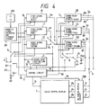
- FIG.4 A still another preferred embodiment of the present invention is illustrated in Fig.4.
- reference numeral 30 denotes a control circuit, i.e. a control circuit 81 having a function to generate characters or figure information to be displayed on the screen
- reference numeral 91 denotes a power supply switch
- 500 denotes an on-screen display circuit
- 3e denotes an on-screen display signal
- 3f denotes control signals of the power supply switches 81 and 91
- Ro, Go and Bo denote a primary color singal including the on-screen information.
- the on-screen display circuit 500 may display the information such as a mode of the playing-back signal 1a during a playing-back operation, for example, in response to the on-screen display signal 3e.
- the control circuit 30 may change over the power supply switches 81 and 91 with the control signal 3f so as to prohibit the power supply from being applied to all the video signal circuits and the croma-video signal circuits 50, 51 and 52 of the NTSC mode, PAL mode and SECAM mode.
- the control circuit 30 may output the on-screen displaying signal 3e to the on-screen displaying circuit 500.
- the on-screen displaying circuit 500 may cause the liquid crystal display device 7 to display in response to the content of the applied on-screen display signal 3e.
- An arrangement position of the on-screen display circuit 500 is not limited to the location shown in Fig. 4, but it may be arranged before or at the middle of or after the NTSC, PAL, SECAM mode video signal circuits 10, 11 and 12 and further it may be arranged at the middle of or after the output of the switch or NTSC, PAL, SECAM croma-video signal circuits 50, 51 and 52, respectively.
- One of the preferred embodiments will be illustrated in Fig. 10 and described later.
- Fig.5 is illustrated one example of a configuration of an active matrix mode displaying device of the liquid crystal displaying device 7.
- Reference numeral 71 denotes a displaying control circuit, 71a a horizontal driving control circuit, 71ba vertical scanning control signal, 72 a polarity alternating circuit, 72a a polarity alternating singal, 73 a horizontal driving circuit, 730 a horizontal driving electrode, 74 a vertical scanning circuit, 740 a vertical scanning electrode, 75 a displaying part, 76 a MOS transistor, 77 a liquid crystal element, 78 a common electrode for applying the same electrical potential to all the liquid crystal elements 77.
- the primary color signals Ro, Go, Bo applied the polarity alternating circuit 72 are reversed at their polarities, and the polarity alternating signals 72a of a positive polarity and a negative polarity are applied to the horizontal driving circuit 73.
- the displaying control circuit 71 may form the horizontal driving signal 71a and the vertical scanning signal 71b in response to the applied displaying control signal, apply them to the horizontal driving circuit 73 and the vertical scanning circuit 74 as as to control their operations.
- the horizontal driving circuit 73 may sample the polarity alternating signal 72a applied in response to the horizontal driving signal 71a and output the sampled voltage to each of the horizontal driving electrodes 730.
- a voltage is applied in sequence to each of the vertical scanning electrodes 740 by the vertical scanning circuit 74 in response to applied vertical scanning signal 71b so as to perform a vertical scanning operation.
- the MOS transistor 76 becomes ON state when a voltage is applied to the gate through the vertical scanning electrodes 740, thereby the display having the applied signal voltage of the horizontal driving electrode 730 written into the liquid crystal 77 is carried out.
- a specified voltage for use in carrying out a display to the primary color signal Bo of the inputs of the polarity alternating circuit 72, and at the same time a specified voltage for preventing the display may be applied to Ro and Go.
- the input primary color singals Ro, Go and Bo of the liquid crystal displaying device 7 may not necessarily be a video signal including the horizontal synchronous signal shown in Fig. 6.
- any of the croma-video signal circuits 50, 51 and 52 of NTSC, PAL and SECAM modes are not necessarily be operated, but a specified voltage may be supplied as the primary color signals Ro, Go and Bo only for a predetermined period of time required for the display from the on-screen display circuit 500 (In case of the aforesaid blue-back display, the specified voltage may always be applied as the primary color signals Ro, Go and Bo.)
- Fig.7 is a configuration figure for showing a still further preferred embodiment of the present invention.
- a different feature of the preferred embodiment shown in Fig.7 from that of the preferred embodiment shown in Fig.4 consists in the fact that a timing signal 71C is supplied from the displaying control circuit 71 to the control circuit 30.
- the displaying control signal outputted from the control circuit 30 for example, there is a method for using the horizontal and vertical synchronous signals.
- an intensity of a tuner (not shown) input electric field is quite weak, it is not possible to get a positive aforesaid horizontal vertical synchronous signal.
- the timing signal 71c is outputted from the displaying control circuit 71 and this is applied to the control circuit 30, thereby the timing of the on-screen displaying information 3e is coincided with the horizontal driving signal 71a and the vertical scanning signal 71b so as to prevent the displayed content from being disturbed.
- 710 denotes a phase comparator
- 711 denotes an LPF
- 712 denotes a VCO
- Vout denotes an output of VCO
- 713 denotes a frequency divider
- Nout denotes an output of the frequency divider
- 714 denotes a timing signal forming circuit.
- phase comparator signal 3CH a horizontal synchronous signal is applied.
- any signal of the NTSC mode, PAL mode and SECAM mode can be displayed as disclosed in the preferred embodiment shown in Fig. 7, it is preferable to set a free run frequency of VCO 712 by coinciding it with any one of the NTSC mode or PAL mode and SECAM mode due to the fact that NTSC mode shows 15.734 kHz, PAL mode and SECAM mode show 15.625 kHz for the different frequencies of the horizontal synchronous signal 3c.
- Fig. 9 there is a method in which two types of VCO 712 and VCO 715 are provided and the aforesaid two types of VCC 712 and 715 are changed over in response to a signal 3cc showing a system of the playing-back signal 1a. In this case, it may be fixed to any one of them (it may be fixed to any VCO).
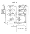
- FIG. 10 A still further preferred embodiment of the present invention is illustrated in Fig. 10.
- a different feature of the preferred embodiment shown in Fig.10 is different from that of Fig.7 consists in the fact that the on-screen information information 3e is not the primary color signals of R, G, B, but is mixed with the complex video signal V. Even in case of the preferred embodiment shown in Fig. 10, the timing signal 71c is outputted to the on-screen display circuit 500, thereby the screen may not be disturbed in case of weak electric field and in case of no signal and then the on-screen display can be performed.
- Fig. 1 the signal distinction corresponding to the signal mode and the recording and playing-back mode is automatically realized by the signal mode distinction circuit 2.
- the aforesaid mode is mechanically specified through a selection of a button or the like.
- the preferred embodiment in this case is shown in Fig. 11.
- reference numeral 20 denotes a signal mode selection switch circuit
- reference numeral 20a denotes a mode distinction signal corresponding to 2a in Fig. 1
- reference numeral 20N denotes a selection switch of NTSC mode signal
- reference numeral 20P denotes a selection switch of PAL mode signal
- reference numeral 20S denotes a selection switch of SECAM mode signal.
- the preferred embodiment is constructed such that the distinction of the signal mode is manually selected by using the signal mode selection switch circuit 20. Even in case of using the configuration shown in Fig. 11, it is possible to perform a changing-over operation between the video signal selection switch 4 and the displaying selection switch 6 in the same manner as that of the preferred embodiments shown in Figs.1 to 10.
- Fig. 11 As regards the mode changing-over operation for SP, LP and EP or the like, the preferred embodiment shown in Fig. 11 can be applied.
- Fig. 12 is a block diagram for showing a still another preferred embodiment of the present invention.
- each of the complex video signals VN, Vp and Vs is directly applied to the NTSC mode, PAL mode and SECAM mode croma-video signal circuits, respectively.
- Applying the circuit shown in Fig. 12 enables the configuration to be simplified more as compared with the case shown in Figs.1 to 11 and at the same time the displaying selection switch 6 is changed over to select the proper signal and to display it.
- Fig.13 is a block diagram for showing a still further preferred embodiment of the present invention and illustrates also the example of the practical configuration of the control circuit 3 shown in Fig. 1.
- reference numeral 31 denotes a controlling part
- 32 denotes a synchronous separating circuit or a synchronous signal forming circuit
- 3d denotes a horizontal synchronous signal
- Vsync denotes a vertical synchronous signal.
- a horizontal synchronous signal is utilized at AGC part or a clamp part, for example, a horizontal synchronous signal is utilized at the clamp part or a burst gate part in case of the croma-video signal circuits 50, 51 and 52, for example, and a horizontal synchronous signal is utilized in the liquid crystal displaying device 7 for use in performing the synchronous scanning operation. Due to this fact, in Fig.
- the aforesaid horizontal synchronous signal is commonly supplied to each of the aforesaid video signal circuits 10, 11, 12 and each of the aforesaid croma-video signal circuits 50, 51, 52 as well as with the aforesaid liquid crystal displaying device 7, thereby each of the aforesaid circuits can be controlled in a substantial same timing and an application of the common circuit enables the configuration to be simplified.
- Fig. 14 is a block diagram for showing a still further preferred embodiment of the present invention and illustrates a practical example of configuration of the control circuit 30 in Fig. 4.
- reference numeral 33 denotes a character and figure information generating circuit.
- the horizontal synchronous signal 3d and the vertical synchronous signal Vsync for use in performing a synchronous scanning are supplied to the liquid crystal displaying device 7 and at the same time applied to the character and figure information generating circuit for use in displaying the on-screen display.
- the liquid crystal displaying device 7 and the character and figure information generating circuit 33 can be operated in a substantial same timing, resulting in that no disturbance in on-screen is found.
- Figs.1 to 14 The preferred embodiments of the present invention have been illustrated in Figs.1 to 14.
- each of the signals 3a, 3b, 3c and 3d has been separately illustrated, and the aforesaid signals 3a, 3b, 3c and 3d may also be combined into one control signal in view of the practical configuration.
- the displaying selection switch 6 has been described as one for changing-over the primary color signals.
- the example of playing-back the video tape of VHS standard has been described and a similar effect can be attained for the case in which signals recorded in the video tape of B standard or 8-mm video standard or other recording media are to be played back.
- the liquid crystal displaying device has been described, and a similar effect can be expected in case that other display devices such as CRT (a cathode ray tube) or a plasma display and the like are used.
- control circuit for controlling an operation of multi-mode video singal recording and playing-back circuit and its output changing-over operation and a control signal can be made in common with the control circuit for controlling a changing-over output of the multi-mode displaying device and the control signal, a size of the circuit can be reduced and at the same time a circuit configuration can be simplified.
- the present invention Since the operation of the circuit not related to the displaying operation can be controlled or stopped by using the common control circuit and the control signal, the present invention has such effects in which the non-required interference can be prevented and the consumption power can be reduced.
Landscapes
- Engineering & Computer Science (AREA)
- Multimedia (AREA)
- Signal Processing (AREA)
- Television Signal Processing For Recording (AREA)
Abstract
Description
- This invention relates to an operation control circuit and an operation control method in a multi-mode displaying device integral with a video signal recording and playback device.
- As described in Japanese Patent Publication No.Sho 64-3391, the prior art device was made such that a multi-mode displaying device was in itself an independent device, a mode discrimination of an input video signal or a changing-over control operation for circuits was performed under a control of an exclusive control circuit provided in the multi-mode displaying device.
- The aforesaid prior art had some problems that there was no arrangement for performing a discrimination of a signal mode again in the multi-mode displaying device, a circuit size was increased and a consumption power was also increased due to the fact that in case of playing-back and displaying a signal recorded in a recording medium under a connection with the multi-mode video signal playing-back device, the aforesaid multi-mode video signal recording and playing-back device discriminated once the mode of signal reproduced from the recording medium and outputted it to the multi-mode displaying device, the aforesaid multi-mode video signal recording and playing-back device and the aforesaid multi-mode displaying device were an independent device, respectively.
- It is an object of the present invention to reduce or simplify a size of a circuit configuration of the aforesaid multi-mode displaying device.
- It is another object of the present invention to reduce a consumption power of the aforesaid multi-mode displaying device.
- In order to accomplish the aforesaid objects, the multi-mode displaying device and the multi-mode video signal recording and playing-back device are made integral to each other, and a circuit for discriminating the video signal modes and various control circuits capable of being commonly utilized are made in common with the aforesaid multi-mode displaying device and the aforesaid multi-mode video signal recording and play-back circuit, respectively.
- In order to accomplish the other objects described above, the multi-mode displaying device and the multi-mode video signal recording and playing-back device are made integral to each other, in which an operation of a circuit not related to the playing-back signal is controlled or stopped by applying a circuit which is common with the aforesaid multi-mode display device and the aforesaid video signal recording and playing-back circuit.
- The multi-mode displaying device and the multi-mode video signal recording and playing-back device are made integral to each other to have a common control circuit, thereby it is not necessary to provide a separate control circuit for each of the aforesaid multi-mode displaying device and the aforesaid multi-mode video signal recording and playing-back circuit and thus a size of the circuit can be reduced. Due to the fact that the common control circuit is utilized, the control signal is commonly applied in the multi-mode displaying device and the multi-mode video signal recording and playing-back circuit so as to simplify the configuration of the device and then the operation modes of the recording and playing-back circuit and the displaying circuit when the playing-back operation is carried out can be positively unified.
- In addition, by applying the aforesaid common control signal to control or stop the operation of non-used circuit, it is possible to reduce a consumption power or eliminate any non-required interference such as beat or the like.
-
- Fig.1 ia a block diagram for showing a multi-mode display device integral with the video signal recording and play-back device acting as one preferred embodiment of the present invention.
- Fig.2 is an illustrative view for showing a recording mode classified by a signal mode in a VHS standard.
- Fig.3 is a block diagram for showing a multi-mode display device integral with a video signal recording and play-back device acting as a second preferred embodiment of the present invention.
- Fig.4 is a block diagram for showing a multi-mode display device integral with a video signal recording and play -back device actiong as a third preferred embodiment of the present invention.
- Fig.5 is a block diagram for showing an example of configuration of a liquid crystal display device in Figs. 1 to 4.
- Fig.6 is a wave-form figure for showing examples of practical wave-forms of primary color signals Ro, Go and Bo in Fig. 4.
- Fig.7 is a block diagram for showing a multi-mode display device integral with a video signal recording and play-back device acting as a fourth preferred embodiment of the present invention.
- Fig.8 is a block diagram for showing an example of a configuration of the displaying control circuit in Fig.7.
- Fig.9 is a block diagram for showing an example of a configuration of the displaying control circuit in Fig.7 which is different from Fig. 8.
- Fig.10 is a block diagram for showing the multi-mode displaying device integral with the video signal recording and play-back device actiong a fifth preferred embodiment of the present invention.
- Figs. 11, 12, 13 and 14 are block diagrams for showing other preferred embodiments of the video signal play-back device of the present invention, respectively.
- Referring now to Fig. 1, one preferred embodiment of the present invention will be described.
- Fig.1 is a block diagram for showing a configuration of a liquid crystal displaying device integral with a video tape recorder (hereinafter called as a liquid crystal displaying device integral with VTR) of the present invention.
- In this figure, in general, a signal processing circuit system before a switch 4 can be considered as a VTR part, and each of the modes of croma-video
signal processing circuits device 7 can be considered as a displaying part, wherein the preferred embodiment shown in Fig.1 illustrates a system in which the aforesaid VTR and the displaying device are substantially made integral to each other. -
Reference numeral 100 denotes a video tape of VHS standard, 1a denotes a playing-back signal of an electrical signal got through a playing-back of a magnetic signal recorded in thevideo tape 100 by a magnetic signal recording and playing-back circuit back signal discriminating circuit signal processing circuits switch 6. 7 denotes a liquid crystal displaying device. - Operation of playing-back and displaying a signal recorded in the
video tape 100 will be described as follows. - A playing-
back signal 1a reproduced from thevideo tape 100 by the magnetic signal recording and playing-back circuit 101 is applied to each of the NTSC mode, PAL mode and SECAM mode videosignal processing circuits discriminating circuit 2. The signal modediscriminating circuit 2 may discriminate the signal as follows, for example. At first, since the NTSC mode has a vertical frequency of 60 Hz, the PAl mode and the SECAM mode have a vertical frequency of 50 Hz, so that a detection of the aforesaid vertical frequency enables a discrimination of whether the mode is an NTSC mode or a PAL mode or an SECAM mode. In addition, the PAL mode and the SECAM mode have different standards for color signals, so that a detection of this difference enables the PAL mode and the SECAM mode to be discriminated. In regards to the VHS standard, each of the NTSC mode, PAL mode and SECAM mode has such a recording mode as one shown in Fig. 2, respectively. The playing-back signal 1a contains information showing which mode of Fig.2 does the aforesaid playing-back signal 1a correspond to. The signal modediscriminating circuit 2 may discriminate the mode of the playing-back signal 1a and output the result of discrimination as adiscriminating signal 2a. - The
discriminating signal 2a is applied to thecontrol circuit 3, and the control circuit may output acontrol signal 3a in response to the aforesaiddiscriminating signal 2a. Each of the videosignal processing circuits back signal 1a in response to thecontrol signal 3a applied so as to otuput a plurality of video signals VN, VP or VS. Operation of the signal processing circuit other than the selected mode at this time may consume not only a non-required electrical power but also cause an interference by a production of non-required signal or an interference of beat, so that it is preferable to terminate the operation of the signal processing circuit other than the selected mode. - The preferred embodiment having this function will be described in detail later in reference to Fig. 2. The aforesaid complex video signals VN, VP and VS are applied to the signal changign-over switch 4. The signal changing-over switch 4 performs a changing-over operation in response to a switch changing-over
signal 3b applied from thecontrol circuit 3 and then any one of the complex video signals VN, VP and VS can be attained as an output complex video signal V of the signal changing-over switch 4. At this time, if the signalmode distinction circuit 2 judges that a playing-back signal 1a is a signal of PA1 mode,thecontrol circuit 3 may apply the changing-oversignal 3b to the signal changing-over switch in response to thedistinction signal 2a indicating the distinction result so as to change-over the signal changing-over switch 4 to enable the complex video signal VP of PAL mode to be attained as the output complex video signal V. - Then, the complex video signal V and the
timing signal 3d are applied to the NTSC mode, PAL mode and SECAM mode croma-video signal circuits video signal circuits video signal circuits video signal circuits switch 6, respectively. The changign-over of the signal changing-overswitch 6 is controlled by the switch changing-oversignal 3b in the same manner as that of the aforesaid signal changing-over switch 4. Accordingly, in case that as described above, the complex video signal VP of PAL mode is got as an output complex video signal V of the signal changing-over switch 4, the changing-over of the signal changing-overswitch 6 is carried out in such a way as the output primary color signals RP, GP, BP of croma-video signal circuits 51 of PAL mode may be attained as an output of the signal changing-overswitch 6. - The output primary color signals R, G, B of the signal changing-over
switch 6 are applied to the liquidcrystal display device 7. Adisplay control signal 3c is simultaneously applied to the aforesaid liquidcrystal display device 7, the liquidcrystal display device 7 may control a display timing in response to the aforesaiddisplay control signal 3c and display in reference to the content of each of the aforesaid primary color signals R, G, and B. - In the above description, the displaying part comprised of a VTR part having as its major part NTSC mode, PAL mode and SF-CAM mode
video signal circuits video signal circuits crystal display device 7 has not an independent separate one to each other, but is a combined one unit, so that a control circuit for use in controlling a changing-over between the signal changing-overswitches 4 and 6 can be used in common between the VTR part and the displaying part, and it is not necessary to provide a control circuit separately for each of the portions, with a result that its configuration can be simplified and at the same time a simple configuration enables a consumption power to be saved. In addition, in case of the PAL mode or SECAM mode where a special playing-back such as a fast feeding search is carried out with a video tape recorded under an LP mode shown in Fig. 2, the colors are not correctly displayed in principle and a quality of display is remarkably deteriorated, so that in case that the aforesaid special playing-back operatino is carried out under the LP mode of PAL or SECAM mode a signal for use in diminishing the colors is outputted as thecontrol signal 3a of an output of thecontrol circuit 3 and then the colors of the displayed image can be diminished and quality of the displayed image can be prevented from being remarkably deteriorated. - Another preferred embodiment of the present invention will be illustrated in Fig. 3. In Fig. 3,
reference numerals - A video signal of PAL mode is recorded in the
video tape 100 and a circuit operation shown in Fig.3 in which the aforesaid PAL video signal is played back will be described. - In Fig. 3, if the signal
mode distinction circuit 2 judges that the playing-back signal 1a applied to the signalmode distinction circuit 2 is a gignal of PAL mode, thecontrol circuit 3 may output the switch changing-oversignal 3b in response to thedistinction signal 2a for indicating the result of distinction. The aforesaid switch changing-oversignal 3b is applied to the signal changing-overswitches 4 and 6 for use in changing-over a complex video signal and a primary color signal to be outputted and also applied to the power supply changing-overswitches signal 3b is applied to the power supply changing-overswitches switches signal 3b is applied to the power supply changing-overswitches switches video signal circuit 11 and the PAL mode croma-video signal circuit 51, respectively. - In case that the replaying-back of the PAL mode video signal is carried out, the power supply is supplied only to the PAL mode
video signal circuit 11 and the PAL mode croma-video signal circuit 51, and then no power supply is supplied to the remaining NTSC mode and SECAM modevideo signal circuits - As described above, since a changing-over of the signal and the power supply changing-over
switches control circuit 3, the configuration can be simplified more as compared with a system in which each of the VTR part and the displaying part is provided with a control circuit and a control signal is supplied for every changing-over switches. - In addition, since the power supply is not supplied to the circuit not requiring any operation, it is possible to reduce the electrical power applied to the VTR part and the displaying part as compared with the case in which all the circuits are operated without being relation to the system of the playing-
back signal 1a. - A still another preferred embodiment of the present invention is illustrated in Fig.4. In Fig.4,
reference numeral 30 denotes a control circuit, i.e. acontrol circuit 81 having a function to generate characters or figure information to be displayed on the screen,reference numeral 91 denotes a power supply switch, 500 denotes an on-screen display circuit, 3e denotes an on-screen display signal, 3f denotes control signals of the power supply switches 81 and 91, and Ro, Go and Bo denote a primary color singal including the on-screen information. The on-screen display circuit 500 may display the information such as a mode of the playing-back signal 1a during a playing-back operation, for example, in response to the on-screen display signal 3e. - In Fig. 4, in case that there is no signal showing no presence of recorded information in the
video tape 100, it is discriminated that no presence of signal is detected by the signalmode distinction circuit 2. Then, the result of distinction is outputted to thecontrol circuit 3 by thedistinction signal 2a. In case that the applieddistinction signal 2a shows no presence of signal, thecontrol circuit 30 may change over the power supply switches 81 and 91 with thecontrol signal 3f so as to prohibit the power supply from being applied to all the video signal circuits and the croma-video signal circuits control circuit 30 may output the on-screen displaying signal 3e to the on-screen displaying circuit 500. The on-screen displaying circuit 500 may cause the liquidcrystal display device 7 to display in response to the content of the applied on-screen display signal 3e. - An arrangement position of the on-
screen display circuit 500 is not limited to the location shown in Fig. 4, but it may be arranged before or at the middle of or after the NTSC, PAL, SECAM modevideo signal circuits video signal circuits - In Fig.5 is illustrated one example of a configuration of an active matrix mode displaying device of the liquid
crystal displaying device 7.Reference numeral 71 denotes a displaying control circuit, 71a a horizontal driving control circuit, 71ba vertical scanning control signal, 72 a polarity alternating circuit, 72a a polarity alternating singal, 73 a horizontal driving circuit, 730 a horizontal driving electrode, 74 a vertical scanning circuit, 740 a vertical scanning electrode, 75 a displaying part, 76 a MOS transistor, 77 a liquid crystal element, 78 a common electrode for applying the same electrical potential to all theliquid crystal elements 77. - In Fig.5, the primary color signals Ro, Go, Bo applied the
polarity alternating circuit 72 are reversed at their polarities, and thepolarity alternating signals 72a of a positive polarity and a negative polarity are applied to thehorizontal driving circuit 73. In turn, the displayingcontrol circuit 71 may form thehorizontal driving signal 71a and thevertical scanning signal 71b in response to the applied displaying control signal, apply them to thehorizontal driving circuit 73 and thevertical scanning circuit 74 as as to control their operations. Thehorizontal driving circuit 73 may sample thepolarity alternating signal 72a applied in response to thehorizontal driving signal 71a and output the sampled voltage to each of thehorizontal driving electrodes 730. A voltage is applied in sequence to each of thevertical scanning electrodes 740 by thevertical scanning circuit 74 in response to appliedvertical scanning signal 71b so as to perform a vertical scanning operation. TheMOS transistor 76 becomes ON state when a voltage is applied to the gate through thevertical scanning electrodes 740, thereby the display having the applied signal voltage of thehorizontal driving electrode 730 written into theliquid crystal 77 is carried out. - In Fig.5, in case that the content of display is not varied in view of time, for example, a so-called blue-back display for displaying a blue color over an entire screen is carried out, a specified voltage for use in carrying out a display to the primary color signal Bo of the inputs of the
polarity alternating circuit 72, and at the same time a specified voltage for preventing the display may be applied to Ro and Go. In this case, the input primary color singals Ro, Go and Bo of the liquidcrystal displaying device 7 may not necessarily be a video signal including the horizontal synchronous signal shown in Fig. 6. That is, in case that only the on-screen display is carried out, any of the croma-video signal circuits - Accordingly, under a condition in which no signal is supplied to the
video tape 100, if the on-screen display is to be carried out, it is not necessary to supply the power to each of the NTSC mode, PAL mode and SECAM modevideo signal circuits video signal circuits - Fig.7 is a configuration figure for showing a still further preferred embodiment of the present invention. A different feature of the preferred embodiment shown in Fig.7 from that of the preferred embodiment shown in Fig.4 consists in the fact that a timing signal 71C is supplied from the displaying
control circuit 71 to thecontrol circuit 30. As the displaying control signal outputted from thecontrol circuit 30, for example, there is a method for using the horizontal and vertical synchronous signals. However, when there is no signal in which no signal is recorded in thevideo tape 100 and when an intensity of a tuner (not shown) input electric field is quite weak, it is not possible to get a positive aforesaid horizontal vertical synchronous signal. Accordingly, it is assumed that in case of performing an on-screen display at these times, a mere output of the on-screen information 3e from thecontrol circuit 30 does not cause a timing of on-screen displaying information to be coincided with a timing between the horizontaldriving control signal 71a and thevertical scanning signal 71b formed by thedisplay control circuit 71 and then the display may be disturbed. - In order to prevent the aforesaid disturbance of display, in case of the preferred embodiment shown in Fig. 7, the
timing signal 71c is outputted from the displayingcontrol circuit 71 and this is applied to thecontrol circuit 30, thereby the timing of the on-screen displaying information 3e is coincided with thehorizontal driving signal 71a and thevertical scanning signal 71b so as to prevent the displayed content from being disturbed. - As a means for forming the timing signals 7a, 7b and 7c required in the displaying
control circuit 71, for example, a method for using PLL circuit shown in Fig. 8. In Fig, 8, 710 denotes a phase comparator, 711 denotes an LPF, 712 denotes a VCO, Vout denotes an output of VCO, 713 denotes a frequency divider, Nout denotes an output of the frequency divider, and 714 denotes a timing signal forming circuit. In Fig. 8, as the phase comparator signal 3CH, a horizontal synchronous signal is applied. In Fig. 8, in case that the horizontal synchronous signal 3CH is applied to thephase comparator 710, phases of the horizontal synchronous signal 3CH is coincided with that of the output Nout of the frequency divider, thereby the phase of the output Vout of VCO is always coincided with the phase of the horizontal synchronous signal 3CH so as to prevent the video image from being disturbed. In turn, in case that there is no signal in which the horizontal synchronous signal 3CH is not applied to thephase comparator 710,VCO 712 is in its free run state, so that a free run oscillation frequency ofVCO 712 is set in advance in such a way as a frequency of the output Nout of the frequency divider is approximately coincided with a frequency of the horizontalsynchronous signal 3c in advance. Provided that if any signal of the NTSC mode, PAL mode and SECAM mode can be displayed as disclosed in the preferred embodiment shown in Fig. 7, it is preferable to set a free run frequency ofVCO 712 by coinciding it with any one of the NTSC mode or PAL mode and SECAM mode due to the fact that NTSC mode shows 15.734 kHz, PAL mode and SECAM mode show 15.625 kHz for the different frequencies of the horizontalsynchronous signal 3c. As shown in Fig. 9, there is a method in which two types ofVCO 712 andVCO 715 are provided and the aforesaid two types ofVCC back signal 1a. In this case, it may be fixed to any one of them (it may be fixed to any VCO). - A still further preferred embodiment of the present invention is illustrated in Fig. 10. A different feature of the preferred embodiment shown in Fig.10 is different from that of Fig.7 consists in the fact that the on-
screen information information 3e is not the primary color signals of R, G, B, but is mixed with the complex video signal V. Even in case of the preferred embodiment shown in Fig. 10, thetiming signal 71c is outputted to the on-screen display circuit 500, thereby the screen may not be disturbed in case of weak electric field and in case of no signal and then the on-screen display can be performed. - In Fig. 1, the signal distinction corresponding to the signal mode and the recording and playing-back mode is automatically realized by the signal
mode distinction circuit 2. However, there is sometimes a case in which the aforesaid mode is mechanically specified through a selection of a button or the like. The preferred embodiment in this case is shown in Fig. 11. In Fig. 11,reference numeral 20 denotes a signal mode selection switch circuit,reference numeral 20a denotes a mode distinction signal corresponding to 2a in Fig. 1,reference numeral 20N denotes a selection switch of NTSC mode signal,reference numeral 20P denotes a selection switch of PAL mode signal and reference numeral 20S denotes a selection switch of SECAM mode signal. - In Fig.11, the preferred embodiment is constructed such that the distinction of the signal mode is manually selected by using the signal mode
selection switch circuit 20. Even in case of using the configuration shown in Fig. 11, it is possible to perform a changing-over operation between the video signal selection switch 4 and the displayingselection switch 6 in the same manner as that of the preferred embodiments shown in Figs.1 to 10. - As regards the mode changing-over operation for SP, LP and EP or the like, the preferred embodiment shown in Fig. 11 can be applied.
- Fig. 12 is a block diagram for showing a still another preferred embodiment of the present invention. In Fig.12, each of the complex video signals VN, Vp and Vs is directly applied to the NTSC mode, PAL mode and SECAM mode croma-video signal circuits, respectively. Applying the circuit shown in Fig. 12 enables the configuration to be simplified more as compared with the case shown in Figs.1 to 11 and at the same time the displaying
selection switch 6 is changed over to select the proper signal and to display it. - Fig.13 is a block diagram for showing a still further preferred embodiment of the present invention and illustrates also the example of the practical configuration of the
control circuit 3 shown in Fig. 1. In Fig. 13,reference numeral 31 denotes a controlling part, 32 denotes a synchronous separating circuit or a synchronous signal forming circuit, 3d denotes a horizontal synchronous signal and Vsync denotes a vertical synchronous signal. - In Fig. 13, in case of the
video signal circuits video signal circuits crystal displaying device 7 for use in performing the synchronous scanning operation. Due to this fact, in Fig. 13, the aforesaid horizontal synchronous signal is commonly supplied to each of the aforesaidvideo signal circuits video signal circuits crystal displaying device 7, thereby each of the aforesaid circuits can be controlled in a substantial same timing and an application of the common circuit enables the configuration to be simplified. - Fig. 14 is a block diagram for showing a still further preferred embodiment of the present invention and illustrates a practical example of configuration of the
control circuit 30 in Fig. 4. In Fig. 14,reference numeral 33 denotes a character and figure information generating circuit. - In Fig. 14, the horizontal
synchronous signal 3d and the vertical synchronous signal Vsync for use in performing a synchronous scanning are supplied to the liquidcrystal displaying device 7 and at the same time applied to the character and figure information generating circuit for use in displaying the on-screen display. With this arrangement, the liquidcrystal displaying device 7 and the character and figureinformation generating circuit 33 can be operated in a substantial same timing, resulting in that no disturbance in on-screen is found. - The preferred embodiments of the present invention have been illustrated in Figs.1 to 14. In Figs.1 to 12, each of the
signals aforesaid signals selection switch 6 has been described as one for changing-over the primary color signals. Even if there is a modification such as a changing-over of a color difference signal (R-Y, G-Y, B-Y) of the NTSC mode, PAL mode and SECAM mode by using the aforesaid displayingselection switch 6, a similar effect as found in the preferred embodiments shown in Figs.1 to 12 can be attained. - In the aforesaid description, the example of playing-back the video tape of VHS standard has been described and a similar effect can be attained for the case in which signals recorded in the video tape of B standard or 8-mm video standard or other recording media are to be played back. As the displaying device, the liquid crystal displaying device has been described, and a similar effect can be expected in case that other display devices such as CRT (a cathode ray tube) or a plasma display and the like are used.
- According to the present invention, since the control circuit for controlling an operation of multi-mode video singal recording and playing-back circuit and its output changing-over operation and a control signal can be made in common with the control circuit for controlling a changing-over output of the multi-mode displaying device and the control signal, a size of the circuit can be reduced and at the same time a circuit configuration can be simplified.
- Since the operation of the circuit not related to the displaying operation can be controlled or stopped by using the common control circuit and the control signal, the present invention has such effects in which the non-required interference can be prevented and the consumption power can be reduced.
Claims (12)
a signal recording and playing-back means composed of a first and a second video signal circuit (10, 11, 12) for playing-back signals recorded on a recording medium (100) and selecting several types of television mode signals played-back from the recording medium (100);
a signal playing-back means composed of a third and a fourth video signal circuit (50, 51, 52) for selecting several types of television mode signals supplied from said signal recording and playing-back means; and
a displaying device (7) for displaying an output signal of said signal playing-back means,
said multi-mode video signal playing-back and displaying device comprising a detection distinction means (2) for detecting a difference in frequencies of synchronous signals contained in the video signal, detecting the television signals having different field frequencies to each other and discriminating them, and a changing-over control circuit (3) for selecting the first and second video signal circuits (10, 11, 12) of said signal recording and playing-back means by the output signal (2a) of said sensing and distinction means (2) and for selecting the third and fourth video signal circuits (50, 51, 52) of said signal playing-back means.
characterized in that
said multi-mode displaying device intergral with the video signal playing-back device comprising a control circuit (3) having a function for terminating an operation of a color signal processing part of said PAL mode or SECAM mode video signal circuit or said croma-video when the signal recorded in an LP mode of the PAL mode in the VHS standard or the SECAM mode, or shielding the output signal and displaying mono-color on the displaying device.
characterized in that
a signal output synchronously separated and detected or synchronously formed is commonly connected with said video signal circuit (10, 11, 12), said croma-video signal circuit (50, 51, 52) and said displaying device (7).
characterized in that
each of the outputs corresponding to each of the signal modes of said several types of video signal circuits (10, 11, 12) is directly connected to several types of croma-video signal circuits (50, 51, 52) having the same signal modes, respectively.
characterized in that
said multi-mode displaying device integral with a video signal playing-back device comprising a scanning control circuit (3, 71) having a function for forming a scanning timing signal (71a, 71b) of said matrix mode displaying device (7) in response to horizontal and vertical synchronous signals (3d, 3CH) and a function for forming a displaying timing signal (71c) of said on-screen displaying circuit (500, 33), wherein said scanning control circuit (3, 71) being commonly connected to said matrix mode displaying device (7) and said on-screen displaying circuit (500, 33).
characterized in that
an on-screen displaying circuit (33, 500) composed of a character and figure information generating circuit (33) and a displaying circuit, and a control circuit (3) having a function for distinguishing an output state of a weak electric field state of said tuner circuit or non-signal state and a function for stopping operations of said video signal circuit (10, 11, 12) and said croma-video signal circuit (50, 51 ,52) are provided, and wherein said matrix displaying device (7) has a scanning timing signal output and said scanning timing signal (71a to 71c) output is connected to said on-screen displaying circuit (500).
Applications Claiming Priority (2)
| Application Number | Priority Date | Filing Date | Title |
|---|---|---|---|
| JP194084/89 | 1989-07-28 | ||
| JP1194084A JP2771266B2 (en) | 1989-07-28 | 1989-07-28 | Multi-system video signal playback and display device |
Publications (2)
| Publication Number | Publication Date |
|---|---|
| EP0410489A2 true EP0410489A2 (en) | 1991-01-30 |
| EP0410489A3 EP0410489A3 (en) | 1992-09-02 |
Family
ID=16318691
Family Applications (1)
| Application Number | Title | Priority Date | Filing Date |
|---|---|---|---|
| EP19900114508 Withdrawn EP0410489A3 (en) | 1989-07-28 | 1990-07-27 | Multi-mode video signal playback and display device |
Country Status (3)
| Country | Link |
|---|---|
| US (1) | US5432612A (en) |
| EP (1) | EP0410489A3 (en) |
| JP (1) | JP2771266B2 (en) |
Cited By (4)
| Publication number | Priority date | Publication date | Assignee | Title |
|---|---|---|---|---|
| EP0488337A2 (en) * | 1990-11-30 | 1992-06-03 | Hitachi, Ltd. | Magnetic recording apparatus |
| EP0533092A2 (en) * | 1991-09-18 | 1993-03-24 | Hitachi, Ltd. | Video camera with switchable aspect ratio |
| EP0687107A2 (en) * | 1994-06-07 | 1995-12-13 | Matsushita Electric Industrial Co., Ltd. | Television receiver incorporating video recording and reproducing apparatus |
| US6463210B1 (en) | 1992-09-11 | 2002-10-08 | Pioneer Corporation | Video disc having an aspect ratio information and video disc player having an aspect ratio converting function |
Families Citing this family (2)
| Publication number | Priority date | Publication date | Assignee | Title |
|---|---|---|---|---|
| JP2003009160A (en) * | 2001-06-27 | 2003-01-10 | Pioneer Electronic Corp | Color format discriminating apparatus and color format discriminating method |
| KR20040067579A (en) * | 2003-01-24 | 2004-07-30 | 삼성전자주식회사 | Back-light driving apparatus of LCD |
Citations (8)
| Publication number | Priority date | Publication date | Assignee | Title |
|---|---|---|---|---|
| US3845237A (en) * | 1973-01-17 | 1974-10-29 | Sony Corp | System for recording and/or reproducing color television signals |
| GB2089167A (en) * | 1980-11-19 | 1982-06-16 | Philips Nv | Television receiver circuit arrangement for identifying the standard |
| FR2543341A1 (en) * | 1983-03-26 | 1984-09-28 | Citizen Watch Co Ltd | TELEVISION RECEIVER USING A LIQUID CRYSTAL MATRIX VIEWING SCREEN |
| US4549224A (en) * | 1982-04-23 | 1985-10-22 | Sony Corporation | Digital video tape recorder that can be used with different television systems |
| US4710826A (en) * | 1985-06-18 | 1987-12-01 | Casio Computer Co., Ltd. | Apparatus with liquid crystal display panel, for recording/playing back television signal by utilizing digital audio tape recorder system |
| JPS63276984A (en) * | 1987-05-08 | 1988-11-15 | Mitsubishi Electric Corp | Character display circuit for character generator of television receiver |
| DE3720353A1 (en) * | 1987-06-19 | 1989-01-05 | Online Tech Datenuebertragungs | Method and circuit arrangement for driving an image reproduction device |
| EP0311442A2 (en) * | 1987-10-08 | 1989-04-12 | Victor Company Of Japan, Limited | Magnetic recording and reproducing apparatus and recording method |
Family Cites Families (8)
| Publication number | Priority date | Publication date | Assignee | Title |
|---|---|---|---|---|
| BE889952A (en) * | 1981-08-12 | 1981-12-01 | Erumba Gotha H | SYSTEM FOR SHARING CIRCUITS FOR TELEVISION AND VIDEOCASSETTE OR VIDEOBAND IN THE SAME HOUSING |
| JPS58139587A (en) * | 1982-02-13 | 1983-08-18 | Mitsubishi Electric Corp | Video reproducer |
| US4694348A (en) * | 1985-06-14 | 1987-09-15 | Citizen Watch Co., Ltd. | Method of driving liquid crystal display panel of TV receiver |
| JPH0719330B2 (en) * | 1985-12-18 | 1995-03-06 | 松下電器産業株式会社 | Video signal recording / reproducing device |
| JPS643391A (en) * | 1987-06-26 | 1989-01-09 | Nippon Kokan Kk | Pipe unit for penetrating to wall |
| JP2638815B2 (en) * | 1987-07-28 | 1997-08-06 | ソニー株式会社 | Disc playback device |
| JP2644797B2 (en) * | 1988-01-25 | 1997-08-25 | 松下電器産業株式会社 | Video tape recorder |
| EP0357080B1 (en) * | 1988-09-02 | 1994-05-11 | Sanyo Electric Co., Ltd. | Phase synchronizing circuit in video signal receiver and method of establishing phase synchronization |
-
1989
- 1989-07-28 JP JP1194084A patent/JP2771266B2/en not_active Expired - Fee Related
-
1990
- 1990-07-27 US US07/558,521 patent/US5432612A/en not_active Expired - Fee Related
- 1990-07-27 EP EP19900114508 patent/EP0410489A3/en not_active Withdrawn
Patent Citations (8)
| Publication number | Priority date | Publication date | Assignee | Title |
|---|---|---|---|---|
| US3845237A (en) * | 1973-01-17 | 1974-10-29 | Sony Corp | System for recording and/or reproducing color television signals |
| GB2089167A (en) * | 1980-11-19 | 1982-06-16 | Philips Nv | Television receiver circuit arrangement for identifying the standard |
| US4549224A (en) * | 1982-04-23 | 1985-10-22 | Sony Corporation | Digital video tape recorder that can be used with different television systems |
| FR2543341A1 (en) * | 1983-03-26 | 1984-09-28 | Citizen Watch Co Ltd | TELEVISION RECEIVER USING A LIQUID CRYSTAL MATRIX VIEWING SCREEN |
| US4710826A (en) * | 1985-06-18 | 1987-12-01 | Casio Computer Co., Ltd. | Apparatus with liquid crystal display panel, for recording/playing back television signal by utilizing digital audio tape recorder system |
| JPS63276984A (en) * | 1987-05-08 | 1988-11-15 | Mitsubishi Electric Corp | Character display circuit for character generator of television receiver |
| DE3720353A1 (en) * | 1987-06-19 | 1989-01-05 | Online Tech Datenuebertragungs | Method and circuit arrangement for driving an image reproduction device |
| EP0311442A2 (en) * | 1987-10-08 | 1989-04-12 | Victor Company Of Japan, Limited | Magnetic recording and reproducing apparatus and recording method |
Non-Patent Citations (2)
| Title |
|---|
| I.E.E.E. TRANSACTIONS ON CONSUMER ELECTRONICS vol. CE-33, no. 3, August 1987, NEW YORK, NY, USA pages 444 - 449; ISHIKUBO ET. AL.: 'LSIs FOR MULTISTANDARD TV RECEIVERS' * |
| PATENT ABSTRACTS OF JAPAN vol. 13, no. 106 (E-726)14 March 1989 & JP-A-63 276 984 ( MITSUBISHI ELECTRIC CORP. ) 15 November 1988 * |
Cited By (11)
| Publication number | Priority date | Publication date | Assignee | Title |
|---|---|---|---|---|
| EP0488337A2 (en) * | 1990-11-30 | 1992-06-03 | Hitachi, Ltd. | Magnetic recording apparatus |
| EP0488337A3 (en) * | 1990-11-30 | 1993-05-19 | Hitachi, Ltd. | Magnetic recording apparatus |
| US5499145A (en) * | 1990-11-30 | 1996-03-12 | Hitachi, Ltd. | Magnetic recording apparatus with capability of recording signals of a plurality of different television systems |
| EP0533092A2 (en) * | 1991-09-18 | 1993-03-24 | Hitachi, Ltd. | Video camera with switchable aspect ratio |
| EP0533092A3 (en) * | 1991-09-18 | 1993-08-25 | Hitachi, Ltd. | Video cameras capable of switching an aspect ratio and view finders for use in the same |
| US5414463A (en) * | 1991-09-18 | 1995-05-09 | Hitachi, Ltd. | Video cameras capable of switching an aspect ratio and view finders for use in the same |
| US6463210B1 (en) | 1992-09-11 | 2002-10-08 | Pioneer Corporation | Video disc having an aspect ratio information and video disc player having an aspect ratio converting function |
| US6968121B2 (en) | 1992-09-11 | 2005-11-22 | Pioneer Electronic Corporation | Video disc having an aspect ratio information and video disc player having an aspect ratio converting function |
| EP0687107A2 (en) * | 1994-06-07 | 1995-12-13 | Matsushita Electric Industrial Co., Ltd. | Television receiver incorporating video recording and reproducing apparatus |
| EP0687107A3 (en) * | 1994-06-07 | 1996-07-31 | Matsushita Electric Ind Co Ltd | Television receiver incorporating video recording and reproducing apparatus |
| CN1086092C (en) * | 1994-06-07 | 2002-06-05 | 松下电器产业株式会社 | TV with recording and playing device |
Also Published As
| Publication number | Publication date |
|---|---|
| JP2771266B2 (en) | 1998-07-02 |
| JPH0360288A (en) | 1991-03-15 |
| EP0410489A3 (en) | 1992-09-02 |
| US5432612A (en) | 1995-07-11 |
Similar Documents
| Publication | Publication Date | Title |
|---|---|---|
| EP0096628B1 (en) | Apparatus for combining a video signal with graphics and text from a computer | |
| EP0096627B1 (en) | Interactive computer-based information display system | |
| US5638485A (en) | Video signal processing apparatus for processing video signals with different aspect ratios | |
| US5432612A (en) | Multi-mode video signal playback and display device | |
| US5502487A (en) | Character signal display for a camcorder using existent synchronization signals for character display | |
| JP3141404B2 (en) | System determination method for input video signal of multi-scan monitor and multi-scan monitor | |
| JP2508610B2 (en) | Automatic white balance adjustment circuit | |
| JP2868366B2 (en) | Back screen display method and apparatus using on-screen signal | |
| JPH05199462A (en) | Video signal processing circuit | |
| JPH0695766B2 (en) | Automatic white balance adjustment circuit | |
| KR960042655A (en) | Reference Frequency Switching Circuit of Multi Video Cassette Recorder | |
| JPS60153289A (en) | Mode display device of video reproducer | |
| KR920001160B1 (en) | On-screen display recording method for vtr | |
| JP3235423B2 (en) | Clogging detection device for magnetic recording and playback devices | |
| JPS63142780A (en) | Character signal generating device | |
| KR19980034756A (en) | Video playback device with color adjustment for OSD (ON-SCREEN DISPLAY) characters | |
| JPH06233235A (en) | Unwanted signal recording blocking device | |
| JPH09139896A (en) | Automatic screen setting circuit | |
| JPH07231406A (en) | Slave screen display circuit with caption moving function | |
| JPS63149978A (en) | Character video signal generator | |
| JPH11113017A (en) | Signal changeover circuit | |
| JPH066714A (en) | Monitoring device | |
| KR19980015720A (en) | How to select the mode according to the video method in multi-video cassette record | |
| JPH04343594A (en) | Reproducing device | |
| KR980011196A (en) | How to display menu of V |
Legal Events
| Date | Code | Title | Description |
|---|---|---|---|
| PUAI | Public reference made under article 153(3) epc to a published international application that has entered the european phase |
Free format text: ORIGINAL CODE: 0009012 |
|
| 17P | Request for examination filed |
Effective date: 19900809 |
|
| AK | Designated contracting states |
Kind code of ref document: A2 Designated state(s): DE FR GB IT |
|
| PUAL | Search report despatched |
Free format text: ORIGINAL CODE: 0009013 |
|
| AK | Designated contracting states |
Kind code of ref document: A3 Designated state(s): DE FR GB IT |
|
| 17Q | First examination report despatched |
Effective date: 19950131 |
|
| GRAG | Despatch of communication of intention to grant |
Free format text: ORIGINAL CODE: EPIDOS AGRA |
|
| STAA | Information on the status of an ep patent application or granted ep patent |
Free format text: STATUS: THE APPLICATION HAS BEEN WITHDRAWN |
|
| 18W | Application withdrawn |
Withdrawal date: 19960514 |