EP0410295A2 - Single-ended chopper stabilized operational amplifier - Google Patents
Single-ended chopper stabilized operational amplifier Download PDFInfo
- Publication number
- EP0410295A2 EP0410295A2 EP90113802A EP90113802A EP0410295A2 EP 0410295 A2 EP0410295 A2 EP 0410295A2 EP 90113802 A EP90113802 A EP 90113802A EP 90113802 A EP90113802 A EP 90113802A EP 0410295 A2 EP0410295 A2 EP 0410295A2
- Authority
- EP
- European Patent Office
- Prior art keywords
- coupled
- chopper
- field effect
- effect transistor
- input
- Prior art date
- Legal status (The legal status is an assumption and is not a legal conclusion. Google has not performed a legal analysis and makes no representation as to the accuracy of the status listed.)
- Granted
Links
- 238000000034 method Methods 0.000 claims abstract description 11
- 230000005669 field effect Effects 0.000 claims description 66
- 230000008878 coupling Effects 0.000 claims description 3
- 238000010168 coupling process Methods 0.000 claims description 3
- 238000005859 coupling reaction Methods 0.000 claims description 3
- 230000000295 complement effect Effects 0.000 description 4
- 230000006641 stabilisation Effects 0.000 description 4
- 238000011105 stabilization Methods 0.000 description 4
- 238000010586 diagram Methods 0.000 description 2
- 239000004065 semiconductor Substances 0.000 description 2
- 230000032683 aging Effects 0.000 description 1
- 230000008859 change Effects 0.000 description 1
- 230000003247 decreasing effect Effects 0.000 description 1
- 238000005516 engineering process Methods 0.000 description 1
- 230000006872 improvement Effects 0.000 description 1
- 238000004519 manufacturing process Methods 0.000 description 1
- 229910044991 metal oxide Inorganic materials 0.000 description 1
- 150000004706 metal oxides Chemical class 0.000 description 1
- 238000012544 monitoring process Methods 0.000 description 1
- 238000012856 packing Methods 0.000 description 1
- 230000009467 reduction Effects 0.000 description 1
- 230000017105 transposition Effects 0.000 description 1
Images
Classifications
-
- H—ELECTRICITY
- H03—ELECTRONIC CIRCUITRY
- H03F—AMPLIFIERS
- H03F1/00—Details of amplifiers with only discharge tubes, only semiconductor devices or only unspecified devices as amplifying elements
- H03F1/30—Modifications of amplifiers to reduce influence of variations of temperature or supply voltage or other physical parameters
- H03F1/303—Modifications of amplifiers to reduce influence of variations of temperature or supply voltage or other physical parameters using a switching device
-
- H—ELECTRICITY
- H03—ELECTRONIC CIRCUITRY
- H03F—AMPLIFIERS
- H03F3/00—Amplifiers with only discharge tubes or only semiconductor devices as amplifying elements
- H03F3/45—Differential amplifiers
- H03F3/45071—Differential amplifiers with semiconductor devices only
- H03F3/45076—Differential amplifiers with semiconductor devices only characterised by the way of implementation of the active amplifying circuit in the differential amplifier
- H03F3/45179—Differential amplifiers with semiconductor devices only characterised by the way of implementation of the active amplifying circuit in the differential amplifier using MOSFET transistors as the active amplifying circuit
- H03F3/45183—Long tailed pairs
- H03F3/45192—Folded cascode stages
-
- H—ELECTRICITY
- H03—ELECTRONIC CIRCUITRY
- H03F—AMPLIFIERS
- H03F3/00—Amplifiers with only discharge tubes or only semiconductor devices as amplifying elements
- H03F3/45—Differential amplifiers
- H03F3/45071—Differential amplifiers with semiconductor devices only
- H03F3/45479—Differential amplifiers with semiconductor devices only characterised by the way of common mode signal rejection
- H03F3/45632—Differential amplifiers with semiconductor devices only characterised by the way of common mode signal rejection in differential amplifiers with FET transistors as the active amplifying circuit
- H03F3/45744—Differential amplifiers with semiconductor devices only characterised by the way of common mode signal rejection in differential amplifiers with FET transistors as the active amplifying circuit by offset reduction
- H03F3/45775—Differential amplifiers with semiconductor devices only characterised by the way of common mode signal rejection in differential amplifiers with FET transistors as the active amplifying circuit by offset reduction by using cross switches
-
- H—ELECTRICITY
- H03—ELECTRONIC CIRCUITRY
- H03F—AMPLIFIERS
- H03F2200/00—Indexing scheme relating to amplifiers
- H03F2200/81—Inputs or outputs are crossed during a first switching time, not crossed during a second switching time
Definitions
- This invention relates in general to the field of chopper stabilized operational amplifiers and, more particularly, to a single ended operational amplifier having an improved offset voltage using new chopper stabilization techniques which reduces noise and improves bandwidth.
- Operational amplifiers are widely used in the electronics industry because of their many excellent circuit characteristics including high open loop gain, high input impedance, and low output impedance.
- General applications of the operational amplifier include circuit configurations such as voltage and current amplifiers, differentiators and integrators, active filters, oscillators, and analog to digital and digital to analog converters.
- operational amplifiers are used in conjunction with positive and or negative feedback in combination with passive and or active elements.
- An operational amplifier is also widely used to function as a voltage comparator, wherein typically, a reference signal is applied to the inverting input and the voltage to be compared is applied to the noninverting input. If the magnitude of the voltage to be compared is greater than the magnitude of the reference signal, the output of the comparator substantially equals the positive supply voltage. If the magnitude of the voltage to be compared is less than the magnitude of the reference voltage, the output of the comparator substantially equals the negative or ground supply voltage.
- An inverted voltage comparator may be provided by simply transposing the signals at the inverting and noninverting inputs. Using the operational amplifier as a voltage comparator requires no external components or feedback, and its output only has two states of high and low.
- the operational amplifier as utilized in the realization of a variety of circuit functions may be manufactured in bipolar or Complementary Metal Oxide Semiconductor (CMOS) technology or some combination thereof.
- CMOS Complementary Metal Oxide Semiconductor
- the CMOS implementation is desirable for its high packing density and low power consumption characteristics.
- operational amplifiers are increasingly being integrated onto chips which merge digital and analog functions together with an increasing number of devices.
- a typical problem associated with operational amplifiers is that of an offset error voltage. This type of error appears as deviations in the expected output due to imbalances in the input stage. This is further due to statistical deviations between the devices of the inverting and noninverting inputs. While this offset error is correctable by null offset adjustment, it requires additional circuitry and adds to the manufacturing time. A secondary problem often associated with null offset adjustment is a resulting decrease in the operational amplifier's input common mode range.
- null offset adjustment was to trim a resistor on the integrated circuit itself by a laser beam while applying input signals and monitoring the output. This method improves the temperature coefficient problem but requires the additional circuitry, expensive laser beam equipment, reduction in input common mode range, adjustment time, and text fixtures. Due to the aging of the semiconductor, null offset adjustments may drift with no means available to readjust.
- an improved method of reducing the null offset error is available by using chopper stabilization techniques.
- This technique uses a chopper at the input of a first fully differential operational amplifier in order to alternate the application of the inverting and noninverting input signals (transpose) to the first fully differential operational amplifier at some frequency which is at least twice the frequency of the input signal frequency.
- the outputs of the first fully differential operational amplifier are input into a second chopper for alternating the application of the output signals to a second fully differential operational amplifier.
- the offset error is reduced because the error is reversed on each transposition of the input and output signals, therein allowing the error due to device mismatches to cancel out. While this technique reduces the offset error, it has the disadvantages of limiting the bandwidth to typically less than 50 kilohertz, introducing switching noise, and requiring fully differential operational amplifiers.
- an operational amplifier having an improved offset voltage, comprising a switching circuit coupled between first and second input signals for alternately transposing the coupling of the first and second input signals to a differential input stage that is coupled to the switching circuit.
- the switching is made at a predetermined frequency being at least twice the frequency of the input signals.
- An output stage of the operational amplifier is coupled to the differential input stage and coupled to an output terminal having first and second currents, wherein the first and second currents are alternately provided at the output terminal at the predetermined frequency by at least one more switching circuit.
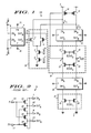
- a single ended, chopper stabilized operational amplifier 20 is shown in FIG. 1 comprising a chopper circuit 9 having input terminals 7 and 8 connected for receiving the input voltages V IN (+) and V IN (-), respectively, at IN A and IN B , respectively.
- the chopper 9 has control terminals 10 and 11 connected for receiving complementary control signals F and F B , respectively, and output nodes 12 and 13 for providing chopper signals OUT A and OUT B respectively.
- the chopper circuit 9 is shown in more detail in FIG. 2.
- the chopper 9 comprises field effect transistors 31,32, 33, and 34 wherein the field effect transistor 31 has a source connected to the input terminal 7, a gate connected to the control terminal 10, and a drain connected to the output node 12.
- the field effect transistor 32 has a source connected to the output node 12, a gate connected to the control terminal 11, and a drain connected to the input terminal 8.
- the field effect transistor 33 has a source connected to the input terminals, a gate connected to the control terminal 10, and a drain connected to the output node 13.
- the field effect transistor 34 has a source connected to the output node 13, a gate connected to the control terminal 11, and a drain connected to the input terminal 7.
- control signal F When the control signal F is high, the control signal F B is low and the field effect transistors 31 and 33 are on, thereby providing a low resistance path between IN A and OUT A , and between IN B and OUT B , respectively.
- the field effect transistors 32 and 33 are off therein isolating IN A from OUT B , and isolating IN B from OUT A .
- control signal F When control signal F is low, the low resistance path is transposed so that the signal at IN A appears at OUT B , and the signal at IN B appears at OUT A .
- a differential input stage 35 includes field effect transistors 3, 4, 5, and 6 with the gates of the differential field effect transistors 3 and 4 providing noninverting and inverting inputs, respectively, and connected to the output nodes 12 and 13, respectively.
- the field effect transistors has a drain connected to the drains of the field effect transistors 3 and 4, and a gate connected for receiving a BIAS2 signal.
- the field effect transistor 6 has a drain connected to a source of the field effect transistor 5, a gate connected for receiving a BIAS1 signal, and a source connected to a supply voltage terminal 2 for receiving the ground supply voltage.
- the chopper circuit 9 causes the input signals V IN (+) and V IN (-) to alternately be applied to the noninverting and inverting inputs of the differential input stage 35.
- Field effect transistors 14 and 15 form a current mirror for providing currents I1 and I2, respectively, responsive to the input signals V IN (+) and V IN (-).
- the source of the field effect transistor 14 is connected to a supply voltage terminal 1 for receiving a positive supply voltage, a gate is connected to a node A, and a drain is connected to the source of the field effect transistor 3.
- the source of the field effect transistor 15 is connected to the supply voltage terminal 1 for receiving the positive supply voltage, a gate is connected to the gate of the field effect transistor 14, and a drain is connected to the source of the field effect transistor 4.
- a chopper 16 has an IN A input connected to the drain of the field effect transistor 14, and an IN A input connected to the drain of the field effect transistor 15.
- the control inputs F and F B are connected for receiving the complementary control signals F and F B .
- the chopper 16 alternately transposes the currents I1 and I2 to first and second current paths formed by the field effect transistors 17 and 21, and 18 and 22, respectively.
- the field effect transistors 17, 18, 21, and 22 form an output stage 36 for providing an output signal, V OUT , at an output terminal 23.
- the field effect transistor 17 has a source connected to an OUT A node of the chopper 16, a gate connected for receiving a BIAS3 signal, and a drain connected to the node A.
- the field effect transistor 18 has a source connected to an OUT B node of the chopper 16, a gate connected for receiving the BIAS3 signal, and a drain connected to the output terminal 23.
- the field effect transistor 21 has a drain connected to the node A and a gate connected for receiving the BIAS2 signal.
- the field effect transistor 22 has a drain connected to the output terminal 23 and a gate connected for receiving the BIAS2 signal.
- a chopper 24 has its inputs IN A and IN B connected to the sources of the field effect transistors 21 and 22, respectively, for again alternately transposing the currents I1 and I2 before reaching a load stage 37 made up of the field effect transistors 25 and 26.
- the chopper 24 has its control terminals F and F B connected for receiving the complementary control signals F and F B , respectively.
- the field effect transistors 25 and 26 have their drains connected to the output nodes OUT A and OUT B respectively of the chopper 24, their gates connected for receiving the BIAS1 signal, and their sources connected to the supply voltage terminal 2.
- the load stage 37 provides the single ended output terminal 23 with a reference point to the ground supply voltage.
- the control signal F Is high (FB is low) the input signals V IN (+) and V IN (-) are applied to the noninverting and inverting inputs (the gates of the field effect transistors 3 and 4, respectively) of the differential input stage 35 which determines the relative magnitudes of the currents Ij and I2 respectively.
- the current I2 flows through the first current path formed by the field effect transistors 17, 21, and 25, and the current I1 flows through the second current path formed by the transistors 18, 22, and 26. This in turn determines the magnitude of the output voltage V OUT .
- the control signals F and F B have a frequency of at least twice the frequency of the input signals V IN (+) and V IN (-) in order to satisfy the Nyquist criteria therein avoiding aliasing problems. It is important that the choppers 9, 16, and 24 switch together but their relative phases may changed (i.e., chopper 9 could have its F and F B inputs transposed).
- the magnitude of the current I1 is now determined by input signal V IN (-) and the magnitude of the current I2 is determined by input signal V IN (+).
- the current 12 now flows through the second current path in the output stage 36 and switches back to the first current path in the load stage 37. Also the current I1 flows through the first current path of the output stage 36 and switches back to the second current path when it reaches the load stage 37.
- the offset error is created by mismatches in the field effect transistor pairs 3 and 4, 14 and 15, 17 and 18, 21 and 22, and 25 and 26.
- the chopper stabilized, single ended operational amplifier 20 not only reduces the offset error, but also provides a further improvement by decreasing the switching noise. This is because the field effect transistors 17, 18, 21, and 22 are not switched by the choppers 9, 16, and 24.
- the largest voltage differential may exist between the node A and the output terminal 23 and it is the switching of these nodes in conventional chopper stabilized operational amplifiers which introduce most of the switching noise.
- This switching noise for example, is typically on the order of 1 millivolt. Because this is avoided, there is substantially less noise introduced and the frequency of operation can be increased.
- the chopper stabilized, single ended operational amplifier 20 has an improved bandwidth, for example, 1 megahertz. It should be noted that switching noise below the chopper frequency, known as flicker or 1/f noise, is cancelled in this and in conventional chopper stabilized operational amplifiers.
Abstract
Description
- This invention relates in general to the field of chopper stabilized operational amplifiers and, more particularly, to a single ended operational amplifier having an improved offset voltage using new chopper stabilization techniques which reduces noise and improves bandwidth.
- Operational amplifiers are widely used in the electronics industry because of their many excellent circuit characteristics including high open loop gain, high input impedance, and low output impedance. General applications of the operational amplifier include circuit configurations such as voltage and current amplifiers, differentiators and integrators, active filters, oscillators, and analog to digital and digital to analog converters. To realize these different circuit configurations, operational amplifiers are used in conjunction with positive and or negative feedback in combination with passive and or active elements.
- An operational amplifier is also widely used to function as a voltage comparator, wherein typically, a reference signal is applied to the inverting input and the voltage to be compared is applied to the noninverting input. If the magnitude of the voltage to be compared is greater than the magnitude of the reference signal, the output of the comparator substantially equals the positive supply voltage. If the magnitude of the voltage to be compared is less than the magnitude of the reference voltage, the output of the comparator substantially equals the negative or ground supply voltage. An inverted voltage comparator may be provided by simply transposing the signals at the inverting and noninverting inputs. Using the operational amplifier as a voltage comparator requires no external components or feedback, and its output only has two states of high and low.
- The operational amplifier as utilized in the realization of a variety of circuit functions may be manufactured in bipolar or Complementary Metal Oxide Semiconductor (CMOS) technology or some combination thereof. The CMOS implementation is desirable for its high packing density and low power consumption characteristics. Also, operational amplifiers are increasingly being integrated onto chips which merge digital and analog functions together with an increasing number of devices.
- A typical problem associated with operational amplifiers is that of an offset error voltage. This type of error appears as deviations in the expected output due to imbalances in the input stage. This is further due to statistical deviations between the devices of the inverting and noninverting inputs. While this offset error is correctable by null offset adjustment, it requires additional circuitry and adds to the manufacturing time. A secondary problem often associated with null offset adjustment is a resulting decrease in the operational amplifier's input common mode range.
- Early operational amplifiers provided additional pins to which a variable resistor could be connected for making a null offset adjustment. This had the disadvantages of requiring additional pins on the operational amplifier integrated circuit therein increasing its cost, requiring the additional resistor or trim potentiometer, and increasing the size of the printed circuit board. Also, the operational amplifier and trim potentiometer had different temperature coefficients and would not track over temperature changes causing the null offset to drift. An improved method of null offset adjustment is to trim a resistor on the integrated circuit itself by a laser beam while applying input signals and monitoring the output. This method improves the temperature coefficient problem but requires the additional circuitry, expensive laser beam equipment, reduction in input common mode range, adjustment time, and text fixtures. Due to the aging of the semiconductor, null offset adjustments may drift with no means available to readjust.
- If fully differential operational amplifiers are available, versus single ended, an improved method of reducing the null offset error is available by using chopper stabilization techniques. This technique uses a chopper at the input of a first fully differential operational amplifier in order to alternate the application of the inverting and noninverting input signals (transpose) to the first fully differential operational amplifier at some frequency which is at least twice the frequency of the input signal frequency. The outputs of the first fully differential operational amplifier are input into a second chopper for alternating the application of the output signals to a second fully differential operational amplifier. The offset error is reduced because the error is reversed on each transposition of the input and output signals, therein allowing the error due to device mismatches to cancel out. While this technique reduces the offset error, it has the disadvantages of limiting the bandwidth to typically less than 50 kilohertz, introducing switching noise, and requiring fully differential operational amplifiers.
- Thus, what is needed is a single ended operational amplifier having an improved offset voltage using chopper stabilization techniques which reduces switching noise and improves bandwidth.
- Accordingly, it is an object of the present invention to provide an improved chopper stabilized, single ended operational amplifier.
- It is further an object of the present invention to provide a chopper stabilized operational amplifier having reduced noise.
- It is yet a further object of the present invention to provide a chopper stabilized operational amplifier having improved bandwidth.
- In carrying out the above and other objects of the invention in one form, there is provided an operational amplifier having an improved offset voltage, comprising a switching circuit coupled between first and second input signals for alternately transposing the coupling of the first and second input signals to a differential input stage that is coupled to the switching circuit. The switching is made at a predetermined frequency being at least twice the frequency of the input signals. An output stage of the operational amplifier is coupled to the differential input stage and coupled to an output terminal having first and second currents, wherein the first and second currents are alternately provided at the output terminal at the predetermined frequency by at least one more switching circuit.
- The above and other objects, features, and advantages of the present invention will be better understood from the following detailed description taken in conjunction with the accompanying drawings.
-
- FIG. 1 is a schematic diagram of the present invention.
- FIG. 2 is a schematic diagram of a chopper circuit.
- A single ended, chopper stabilized
operational amplifier 20 is shown in FIG. 1 comprising achopper circuit 9 havinginput terminals chopper 9 hascontrol terminals output nodes chopper circuit 9 is shown in more detail in FIG. 2. - Referring to FIG. 2, the
chopper 9 comprisesfield effect transistors field effect transistor 31 has a source connected to theinput terminal 7, a gate connected to thecontrol terminal 10, and a drain connected to theoutput node 12. Thefield effect transistor 32 has a source connected to theoutput node 12, a gate connected to thecontrol terminal 11, and a drain connected to theinput terminal 8. Thefield effect transistor 33 has a source connected to the input terminals, a gate connected to thecontrol terminal 10, and a drain connected to theoutput node 13. Thefield effect transistor 34 has a source connected to theoutput node 13, a gate connected to thecontrol terminal 11, and a drain connected to theinput terminal 7. When the control signal F is high, the control signal FB is low and thefield effect transistors field effect transistors - A
differential input stage 35 includesfield effect transistors 3, 4, 5, and 6 with the gates of the differentialfield effect transistors 3 and 4 providing noninverting and inverting inputs, respectively, and connected to theoutput nodes field effect transistors 3 and 4, and a gate connected for receiving a BIAS₂ signal. The field effect transistor 6 has a drain connected to a source of the field effect transistor 5, a gate connected for receiving a BIAS₁ signal, and a source connected to asupply voltage terminal 2 for receiving the ground supply voltage. Thechopper circuit 9 causes the input signals VIN(+) and VIN(-) to alternately be applied to the noninverting and inverting inputs of thedifferential input stage 35. -
Field effect transistors field effect transistor 14 is connected to asupply voltage terminal 1 for receiving a positive supply voltage, a gate is connected to a node A, and a drain is connected to the source of thefield effect transistor 3. The source of thefield effect transistor 15 is connected to thesupply voltage terminal 1 for receiving the positive supply voltage, a gate is connected to the gate of thefield effect transistor 14, and a drain is connected to the source of the field effect transistor 4. Achopper 16 has an INA input connected to the drain of thefield effect transistor 14, and an INA input connected to the drain of thefield effect transistor 15. The control inputs F and FB are connected for receiving the complementary control signals F and FB. Thechopper 16 alternately transposes the currents I₁ and I₂ to first and second current paths formed by thefield effect transistors chopper 16 is equivalent to thechopper 9 with the exception that all of the devices making up thechopper 16 are P-type devices. As a result, when the control signal F is high, OUTA = INB and OUTB = INA in thechopper 16 which is the opposite state of that for thechopper 9. - The
field effect transistors output stage 36 for providing an output signal, VOUT, at anoutput terminal 23. Thefield effect transistor 17 has a source connected to an OUTA node of thechopper 16, a gate connected for receiving a BIAS₃ signal, and a drain connected to the node A. Thefield effect transistor 18 has a source connected to an OUTB node of thechopper 16, a gate connected for receiving the BIAS₃ signal, and a drain connected to theoutput terminal 23. Thefield effect transistor 21 has a drain connected to the node A and a gate connected for receiving the BIAS₂ signal. Thefield effect transistor 22 has a drain connected to theoutput terminal 23 and a gate connected for receiving the BIAS₂ signal. - A
chopper 24 has its inputs INA and INB connected to the sources of thefield effect transistors load stage 37 made up of thefield effect transistors chopper 24 has its control terminals F and FB connected for receiving the complementary control signals F and FB, respectively. Thefield effect transistors chopper 24, their gates connected for receiving the BIAS₁ signal, and their sources connected to thesupply voltage terminal 2. Theload stage 37 provides the single endedoutput terminal 23 with a reference point to the ground supply voltage. - In operation, when the control signal F Is high (FB is low) the input signals VIN(+) and VIN(-) are applied to the noninverting and inverting inputs (the gates of the
field effect transistors 3 and 4, respectively) of thedifferential input stage 35 which determines the relative magnitudes of the currents Ij and I₂ respectively. The current I₂ flows through the first current path formed by thefield effect transistors transistors choppers chopper 9 could have its F and FB inputs transposed). - When the
choppers output stage 36 and switches back to the first current path in theload stage 37. Also the current I₁ flows through the first current path of theoutput stage 36 and switches back to the second current path when it reaches theload stage 37. The offset error is created by mismatches in the field effect transistor pairs 3 and 4, 14 and 15, 17 and 18, 21 and 22, and 25 and 26. By transposing the input signals VIN(+) and VIN(-) and the currents I₁ and I₂ the offset error caused by the field effect transistor pairs 3 and 4,14 and 15, and 25 and 26 cancel each other out. The offset error introduced by the field effect transistor pairs 17 and 18, and 21 and 22 still exists, but it is well known that these devices produce a much smaller error, for example, approximately 50 microvolts. - The chopper stabilized, single ended
operational amplifier 20 not only reduces the offset error, but also provides a further improvement by decreasing the switching noise. This is because thefield effect transistors choppers output terminal 23 and it is the switching of these nodes in conventional chopper stabilized operational amplifiers which introduce most of the switching noise. This switching noise, for example, is typically on the order of 1 millivolt. Because this is avoided, there is substantially less noise introduced and the frequency of operation can be increased. The chopper stabilized, single endedoperational amplifier 20 has an improved bandwidth, for example, 1 megahertz. It should be noted that switching noise below the chopper frequency, known as flicker or 1/f noise, is cancelled in this and in conventional chopper stabilized operational amplifiers. - By now it should be appreciated that there has been provided a single ended operational amplifier having an improved offset voltage using chopper stabilization techniques which reduces noise and improves bandwidth.
Claims (10)
an output terminal (23);
a differential input stage (35) having noninverting and inverting inputs coupled for receiving first and second input signals;
first switching means (9) coupled between said differential input stage and the first and second input signals for alternately transposing the coupling of the first and second input signals to said differential input stage at a predetermined frequency; and
output means (14, 15, 16, 24, 36, 37) coupled to said differential input stage and coupled to said output terminal having first and second currents wherein the first and second currents are alternately provided at said output terminal at the predetermined frequency.
a first field effect transistor (31) having a source coupled for receiving the first input signal, a gate coupled for receiving a chopper signal, and a drain coupled to the noninverting input of said differential input stage;
a second field effect transistor (32) having a source coupled to the noninverting input of said differential input stage, a gate coupled for receiving an inverted chopper signal, and a drain coupled for receiving the second input signal;
a third field effect transistor (33) having a source coupled for receiving the second input signal, a gate coupled to the gate of the first field effect transistor, and a drain coupled to the inverting input of said differential input stage; and
a fourth field effect transistor (34) having a source coupled to the inverting input of said differential input stage, a gate coupled to the gate of said second field effect transistor, and a drain coupled for receiving the first input signal.
current mirror means (14, 15) coupled to said differential input stage for providing the first and second currents;
second switching means (16) coupled to said current mirror means for alternately transposing the first and second currents at said output terminal;
single ended output stage (36) coupled to said second switching means and coupled to said output terminal for providing an output signal;
third switching means (24) coupled to said single ended output stage for receiving the first and second currents and alternately transposing the first and second currents; and
load stage (37) coupled to said third switching means for receiving the first and second currents and for providing a reference to the output signal.
a first input terminal (7) for receiving a first input signal;
a second input terminal (8) for receiving a second input signal;
an output terminal (23);
first chopper means (9) coupled to said first and second input terminals, said first chopper means having first and second states wherein the first state allows the first and second input signals to pass through unchanged, and the second state transposes the coupling of the first and second input signals;
a differential input stage (35) having inverting and noninverting inputs coupled to said first chopper means for receiving the first and second input signals; and
output means (14, 15, 16, 24, 35, 37) coupled to said differential input stage and coupled to said output terminal for providing an output signal, said output means having first and second current paths and further having first and second currents responsive to the first and second input signals, wherein the first and second currents are alternately transposed in said first and second current paths.
a first field effect transistor (31) having a source coupled to said first input terminal, a gate coupled for receiving a chopper signal, and having a drain coupled to the noninverting input of said differential input stage;
a second field effect transistor (32) having a source coupled to the noninverting input of said differential input stage, a gate coupled for receiving an inverted chopper signal, and having a drain coupled to said second input terminal;
a third field effect transistor (33) having a source coupled to said second input terminal, a gate coupled to the gate of said first field effect transistor, and a drain coupled to the inverting input of said differential input stage; and
a fourth field effect transistor (34) having a source coupled to the inverting input of said differential input stage, a gate coupled to the gate of said second field effect transistor, and a drain coupled to said first input terminal.
current mirror means (14, 15) coupled to said differential input stage for providing the first and second currents;
second chopper means (16) coupled to said current mirror means and coupled to said first and second current paths, said second chopper means having first and second states for alternately transposing the first and second currents between said first and second current paths;
third chopper means (24) coupled to said first and second current paths for receiving the first and second currents, said third chopper having first and second states for alternately transposing the first and second currents; and
load means (37) coupled to said third chopper means for providing a reference to the output signal.
an output terminal (23);
first chopper means (9) coupled to said first and second input terminals for receiving the first and second input signals, and having first and second chopper nodes wherein the first and second input signals are coupled to the first and second chopper nodes, respectively, when said first chopper means is in a first state, and the first and second input signals are coupled to the second and first chopper nodes, respectively, when said first chopper means is in a second state, the first and second states being controlled by the chopper signal;
a differential input stage (35) having noninverting and inverting inputs coupled to the first and second chopper nodes, respectively, for receiving the first and second input signals;
current mirror means (14, 15) coupled to said differential input stage for providing first and second currents having magnitudes responsive to the first and second input signals;
second chopper means (16) coupled to said current mirror means for receiving the first and second currents, and having first and second chopper nodes wherein the first and second currents are coupled to the second and first chopper nodes, respectively, when said second chopper means is in a first state, and the first and second currents are coupled to the first and second chopper nodes, respectively, when said second chopper means is in a second state, the first and second states being controlled by the chopper signal;
single ended output means (36) coupled to said second chopper means for receiving the first and second currents and coupled to said output terminal for providing an output signal;
third chopper means (24) coupled to said single ended output means for receiving the first and second currents, and having first and second chopper nodes wherein the first and second currents are coupled to the first and second chopper nodes, respectively, when said third chopper means is in a first state, and the first and second currents are coupled to the second and first chopper nodes, respectively, when said third chopper means is in a second state, the first and second states being controlled by the chopper signal; and
load means (37) coupled to said third chopper means for receiving the first and second currents for providing a reference from a ground supply voltage to the output signal.
a first field effect transistor (31) having a source coupled to said first input terminal, a gate coupled for receiving a chopper signal, and having a drain coupled to the noninverting input of said differential input stage;
a second field effect transistor (32) having a source coupled to the noninverting input of said differential input stage, a gate coupled for receiving an inverted chopper signal, and having a drain coupled to said second input terminal;
a third field effect transistor (33) having a source coupled to said second input terminal, a gate coupled to the gate of said first field effect transistor, and a drain coupled to the inverting input of said differential input stage; and
a fourth field effect transistor (34) having a source coupled to the inverting input of said differential input stage, a gate coupled to the gate of said second field effect transistor, and a drain coupled to said first input terminal.
a fifth field effect transistor (6) having a source coupled to a ground supply voltage, a gate coupled for receiving a first bias voltage, and having a drain;
a sixth field effect transistor (5) having a source coupled to the drain of said fifth field effect transistor, a gate coupled for receiving a second bias voltage, and having a drain;
a seventh field effect transistor (3) having a drain coupled to the drain of said sixth field effect transistor, a gate coupled to the first chopper node of said first chopper means, and a drain coupled to said current mirror means; and
an eighth field effect transistor (4) having a drain coupled to the drain of said sixth field effect transistor, a gate coupled to the second chopper node of said first chopper means, and a drain coupled to said current mirror means.
a ninth field effect transistor (14) having a source coupled for receiving a positive supply voltage, a gate coupled to said single ended output means, and a drain coupled to the source of said seventh field effect transistor and to said second chopper means for providing the first current; and
a tenth field effect transistor (15) having a source coupled for receiving the positive supply voltage, a gate coupled to the gate of said ninth field effect transistor, and a drain coupled to the source of said eighth field effect transistor and to said second chopper means for providing the second current.
Applications Claiming Priority (2)
| Application Number | Priority Date | Filing Date | Title |
|---|---|---|---|
| US07/386,060 US4947135A (en) | 1989-07-28 | 1989-07-28 | Single-ended chopper stabilized operational amplifier |
| US386060 | 1995-02-07 |
Publications (3)
| Publication Number | Publication Date |
|---|---|
| EP0410295A2 true EP0410295A2 (en) | 1991-01-30 |
| EP0410295A3 EP0410295A3 (en) | 1991-10-23 |
| EP0410295B1 EP0410295B1 (en) | 1996-04-10 |
Family
ID=23524001
Family Applications (1)
| Application Number | Title | Priority Date | Filing Date |
|---|---|---|---|
| EP90113802A Expired - Lifetime EP0410295B1 (en) | 1989-07-28 | 1990-07-19 | Single-ended chopper stabilized operational amplifier |
Country Status (3)
| Country | Link |
|---|---|
| US (1) | US4947135A (en) |
| EP (1) | EP0410295B1 (en) |
| DE (1) | DE69026435T2 (en) |
Cited By (2)
| Publication number | Priority date | Publication date | Assignee | Title |
|---|---|---|---|---|
| WO2005081398A1 (en) | 2004-01-22 | 2005-09-01 | Nokia Corporation | Mixer circuit |
| KR100719390B1 (en) * | 2006-07-20 | 2007-05-18 | 노키아 코포레이션 | Mixer circuit |
Families Citing this family (8)
| Publication number | Priority date | Publication date | Assignee | Title |
|---|---|---|---|---|
| US5136255A (en) * | 1991-06-28 | 1992-08-04 | Texas Instruments Incorporated | Amplifier circuit |
| US5206602A (en) * | 1992-04-30 | 1993-04-27 | Hewlett-Packard Company | Biomedical amplifier circuit |
| US5959498A (en) * | 1997-03-03 | 1999-09-28 | National Semiconductor Corporation | Chopper-stabilized operational amplifier including low-noise chopper switch |
| US6125272A (en) * | 1998-09-25 | 2000-09-26 | Motorola, Inc. | Method and apparatus providing improved intermodulation distortion protection |
| DE60233818D1 (en) * | 2001-10-25 | 2009-11-05 | Nxp Bv | OPERATIONAL AMPLIFIER WITH LOCKED INPUT TRANSISTOR PAIR |
| JP4662698B2 (en) * | 2003-06-25 | 2011-03-30 | ルネサスエレクトロニクス株式会社 | Current source circuit and current setting method |
| US7683701B2 (en) * | 2005-12-29 | 2010-03-23 | Cypress Semiconductor Corporation | Low power Bandgap reference circuit with increased accuracy and reduced area consumption |
| JP6399486B2 (en) * | 2014-07-14 | 2018-10-03 | 株式会社エイアールテック | Operational amplifier circuit |
Citations (4)
| Publication number | Priority date | Publication date | Assignee | Title |
|---|---|---|---|---|
| FR2419610A1 (en) * | 1978-03-10 | 1979-10-05 | Cit Alcatel | Low distortion transistor powered amplifier - has three, four-transistor chopper circuits fed by logic AND=gates |
| GB2022951A (en) * | 1978-06-01 | 1979-12-19 | Intersil Inc | Commutating signal level translator |
| US4360784A (en) * | 1980-08-13 | 1982-11-23 | Automation Systems, Inc. | Transformer coupled isolation amplifier |
| GB2100087A (en) * | 1981-06-10 | 1982-12-15 | Intersil Inc | Chopper-stabilized amplifier |
Family Cites Families (1)
| Publication number | Priority date | Publication date | Assignee | Title |
|---|---|---|---|---|
| US4829263A (en) * | 1988-04-12 | 1989-05-09 | Zdzislaw Gulczynski | High speed instrumentation amplifier with minimized offset voltage and drift |
-
1989
- 1989-07-28 US US07/386,060 patent/US4947135A/en not_active Expired - Lifetime
-
1990
- 1990-07-19 EP EP90113802A patent/EP0410295B1/en not_active Expired - Lifetime
- 1990-07-19 DE DE69026435T patent/DE69026435T2/en not_active Expired - Fee Related
Patent Citations (4)
| Publication number | Priority date | Publication date | Assignee | Title |
|---|---|---|---|---|
| FR2419610A1 (en) * | 1978-03-10 | 1979-10-05 | Cit Alcatel | Low distortion transistor powered amplifier - has three, four-transistor chopper circuits fed by logic AND=gates |
| GB2022951A (en) * | 1978-06-01 | 1979-12-19 | Intersil Inc | Commutating signal level translator |
| US4360784A (en) * | 1980-08-13 | 1982-11-23 | Automation Systems, Inc. | Transformer coupled isolation amplifier |
| GB2100087A (en) * | 1981-06-10 | 1982-12-15 | Intersil Inc | Chopper-stabilized amplifier |
Cited By (3)
| Publication number | Priority date | Publication date | Assignee | Title |
|---|---|---|---|---|
| WO2005081398A1 (en) | 2004-01-22 | 2005-09-01 | Nokia Corporation | Mixer circuit |
| US8023923B2 (en) | 2004-01-22 | 2011-09-20 | Nokia Corporation | Mixer circuit |
| KR100719390B1 (en) * | 2006-07-20 | 2007-05-18 | 노키아 코포레이션 | Mixer circuit |
Also Published As
| Publication number | Publication date |
|---|---|
| EP0410295B1 (en) | 1996-04-10 |
| EP0410295A3 (en) | 1991-10-23 |
| US4947135A (en) | 1990-08-07 |
| DE69026435T2 (en) | 1996-10-31 |
| DE69026435D1 (en) | 1996-05-15 |
Similar Documents
| Publication | Publication Date | Title |
|---|---|---|
| US5187448A (en) | Differential amplifier with common-mode stability enhancement | |
| EP1096671B1 (en) | A differential operational amplifier | |
| EP0663719B1 (en) | Analog filter circuit and semiconductor integrated circuit device using the same | |
| EP1794882B1 (en) | Programmable low noise amplifier and method | |
| KR100299740B1 (en) | Filter circuit | |
| EP0320471B1 (en) | Common mode sensing and control in balanced amplifier chains | |
| WO1991007814A1 (en) | Fully differential cmos power amplifier | |
| EP0037406B1 (en) | Cmos operational amplifier with reduced power dissipation | |
| US7999612B2 (en) | Operational amplifier having DC offset cancellation capability | |
| US20100283527A1 (en) | Analog Switch | |
| EP3736978A1 (en) | Operational amplifier and chip | |
| EP0996996B1 (en) | A high speed and high gain operational amplifier | |
| US7295068B2 (en) | Increasing the linearity of a transconductance cell | |
| US4947135A (en) | Single-ended chopper stabilized operational amplifier | |
| US20080169847A1 (en) | Driver and driver/receiver system | |
| US6819170B1 (en) | Apparatus for sensing differential voltages with high common-mode levels | |
| US4933643A (en) | Operational amplifier having improved digitally adjusted null offset | |
| US6642788B1 (en) | Differential cascode amplifier | |
| Nauta et al. | Analog line driver with adaptive impedance matching | |
| US4868417A (en) | Complementary voltage comparator | |
| EP0655831B1 (en) | High performance transconductance operational amplifier, of the CMOS integrated type | |
| US6542018B1 (en) | Current mode step attenuation control circuit with digital technology | |
| US4706036A (en) | Differential amplifier having ratioed load devices | |
| Caiulo et al. | Video CMOS power buffer with extended linearity | |
| EP1392195B1 (en) | Integrated low-corner frequency high pass filter circuit |
Legal Events
| Date | Code | Title | Description |
|---|---|---|---|
| PUAI | Public reference made under article 153(3) epc to a published international application that has entered the european phase |
Free format text: ORIGINAL CODE: 0009012 |
|
| AK | Designated contracting states |
Kind code of ref document: A2 Designated state(s): DE FR GB IT |
|
| PUAL | Search report despatched |
Free format text: ORIGINAL CODE: 0009013 |
|
| AK | Designated contracting states |
Kind code of ref document: A3 Designated state(s): DE FR GB IT |
|
| 17P | Request for examination filed |
Effective date: 19911104 |
|
| 17Q | First examination report despatched |
Effective date: 19940103 |
|
| GRAA | (expected) grant |
Free format text: ORIGINAL CODE: 0009210 |
|
| GRAH | Despatch of communication of intention to grant a patent |
Free format text: ORIGINAL CODE: EPIDOS IGRA |
|
| AK | Designated contracting states |
Kind code of ref document: B1 Designated state(s): DE FR GB IT |
|
| PG25 | Lapsed in a contracting state [announced via postgrant information from national office to epo] |
Ref country code: IT Free format text: LAPSE BECAUSE OF FAILURE TO SUBMIT A TRANSLATION OF THE DESCRIPTION OR TO PAY THE FEE WITHIN THE PRE;WARNING: LAPSES OF ITALIAN PATENTS WITH EFFECTIVE DATE BEFORE 2007 MAY HAVE OCCURRED AT ANY TIME BEFORE 2007. THE CORRECT EFFECTIVE DATE MAY BE DIFFERENT FROM THE ONE RECORDED.SCRIBED TIME-LIMIT Effective date: 19960410 Ref country code: FR Effective date: 19960410 |
|
| REF | Corresponds to: |
Ref document number: 69026435 Country of ref document: DE Date of ref document: 19960515 |
|
| EN | Fr: translation not filed | ||
| PLBE | No opposition filed within time limit |
Free format text: ORIGINAL CODE: 0009261 |
|
| STAA | Information on the status of an ep patent application or granted ep patent |
Free format text: STATUS: NO OPPOSITION FILED WITHIN TIME LIMIT |
|
| 26N | No opposition filed | ||
| PGFP | Annual fee paid to national office [announced via postgrant information from national office to epo] |
Ref country code: GB Payment date: 20000614 Year of fee payment: 11 |
|
| PG25 | Lapsed in a contracting state [announced via postgrant information from national office to epo] |
Ref country code: GB Free format text: LAPSE BECAUSE OF NON-PAYMENT OF DUE FEES Effective date: 20010719 |
|
| GBPC | Gb: european patent ceased through non-payment of renewal fee |
Effective date: 20010719 |
|
| PGFP | Annual fee paid to national office [announced via postgrant information from national office to epo] |
Ref country code: DE Payment date: 20060731 Year of fee payment: 17 |
|
| PG25 | Lapsed in a contracting state [announced via postgrant information from national office to epo] |
Ref country code: DE Free format text: LAPSE BECAUSE OF NON-PAYMENT OF DUE FEES Effective date: 20080201 |