EP0409906B1 - Device for applying solder - Google Patents
Device for applying solder Download PDFInfo
- Publication number
- EP0409906B1 EP0409906B1 EP89906912A EP89906912A EP0409906B1 EP 0409906 B1 EP0409906 B1 EP 0409906B1 EP 89906912 A EP89906912 A EP 89906912A EP 89906912 A EP89906912 A EP 89906912A EP 0409906 B1 EP0409906 B1 EP 0409906B1
- Authority
- EP
- European Patent Office
- Prior art keywords
- solder
- support sheet
- weakness
- line
- arms
- Prior art date
- Legal status (The legal status is an assumption and is not a legal conclusion. Google has not performed a legal analysis and makes no representation as to the accuracy of the status listed.)
- Expired - Lifetime
Links
- 229910000679 solder Inorganic materials 0.000 title claims abstract description 100
- 239000000463 material Substances 0.000 claims abstract description 27
- 239000000853 adhesive Substances 0.000 claims description 19
- 230000001070 adhesive effect Effects 0.000 claims description 19
- 239000011248 coating agent Substances 0.000 claims description 4
- 238000000576 coating method Methods 0.000 claims description 4
- 230000004907 flux Effects 0.000 claims description 4
- 239000004020 conductor Substances 0.000 abstract description 26
- 239000012858 resilient material Substances 0.000 description 5
- 238000009434 installation Methods 0.000 description 3
- 238000000034 method Methods 0.000 description 3
- 239000004642 Polyimide Substances 0.000 description 2
- 239000004820 Pressure-sensitive adhesive Substances 0.000 description 2
- 238000007598 dipping method Methods 0.000 description 2
- 229920001971 elastomer Polymers 0.000 description 2
- 229920001721 polyimide Polymers 0.000 description 2
- 238000003825 pressing Methods 0.000 description 2
- ATJFFYVFTNAWJD-UHFFFAOYSA-N Tin Chemical compound [Sn] ATJFFYVFTNAWJD-UHFFFAOYSA-N 0.000 description 1
- 230000002411 adverse Effects 0.000 description 1
- 230000000694 effects Effects 0.000 description 1
- 239000000806 elastomer Substances 0.000 description 1
- 238000011065 in-situ storage Methods 0.000 description 1
- 238000007373 indentation Methods 0.000 description 1
- 238000009413 insulation Methods 0.000 description 1
- 239000012774 insulation material Substances 0.000 description 1
- 238000003475 lamination Methods 0.000 description 1
- 238000004519 manufacturing process Methods 0.000 description 1
- 229920002379 silicone rubber Polymers 0.000 description 1
- 239000004945 silicone rubber Substances 0.000 description 1
- 238000005476 soldering Methods 0.000 description 1
- 238000003466 welding Methods 0.000 description 1
Images

Classifications
-
- B—PERFORMING OPERATIONS; TRANSPORTING
- B23—MACHINE TOOLS; METAL-WORKING NOT OTHERWISE PROVIDED FOR
- B23K—SOLDERING OR UNSOLDERING; WELDING; CLADDING OR PLATING BY SOLDERING OR WELDING; CUTTING BY APPLYING HEAT LOCALLY, e.g. FLAME CUTTING; WORKING BY LASER BEAM
- B23K3/00—Tools, devices, or special appurtenances for soldering, e.g. brazing, or unsoldering, not specially adapted for particular methods
- B23K3/06—Solder feeding devices; Solder melting pans
Definitions
- the present invention relates to a device for applying solder to one or more faces of an object, particularly to two opposite faces of an object, in a predetermined location.
- pretinning When it is desired to make a solder connection to an object, it is common first to apply a coating of solder to the object. This process is often referred to as pretinning.
- the object When the connection is to be made to the end of the object, the object may be pretinned by dipping in molten solder, for example as described in the "Soldering Manual" published by the American Welding Society May 1964 page 66. While this method of pretinning has the advantage of being quick and easily controlled, it suffers from the disadvantage that it requires that there be sufficient space around the object for a container for the molten solder. Such space is not always available.
- the object may comprise an electrical conductor which might be fixed at one end and not be sufficiently flexible to be inserted into a container of molten solder.
- the conductor may be a component of a piece of electrical or electronic apparatus.
- the present invention provides a device for applying solder to a face of an object in a predetermined location relative to an edge of the object, without the need for sufficient space around the object for a container for molten solder.
- the invention provides a device for applying solder to a face of an object towards an edge thereof, comprising:
- the device of the invention allows solder to be applied to an object in a predetermined location relative to an edge of the object by engagement of the line of weakness with the said edge.
- the device is particularly applicable to thin objects in which case the line of weakness allows the support sheet to be folded to adopt a U-shape, especially when the arms of the sheet extend substantially parallel away from the line of weakness. In this case, the device will be positioned with one arm of the support sheet on each side of the object.
- the device of the invention is suitable for applying solder to a flat object. It is particularly well suited to applying solder to an array of electrical conductors, especially to the stripped conductors of a multi-conductor electrical cable.
- the conductors of the cable are flat conductors, by which is meant that they have a square or especially rectangular cross-section.
- the device is provided with a quantity of solder on a face of each of the arms of the support sheet.
- a device By folding the support sheet into a U-shape, such a device may be used to apply solder to each of two opposite surfaces of an object.
- the object comprises an array of conductors
- surface tension effects may be relied on to provide solder on more than just the faces of the conductors that are contacted by the device.
- the conductors are flat conductors that are relatively thin, for example less than 0.5 mm thick, it is possible to obtain a solder coating around the entire periphery of each conductor.
- the arrangement of the solder on the two arms of the support sheet is symmetrical so that the arrangement on one of the arms is a mirror-image of that on the other arm.
- the solder may be provided in the form of a continuous tape.
- the tape extends substantially parallel to the line of weakness so that the device can conveniently provide a strip of solder parallel to an edge of the object.
- the solder strip it can be advantageous to have the solder strip arranged at an angle to the edge of the object, in which case the solder tape will extend at an angle of between 0° and 90° to the line of weakness.
- solder When it is desired to provide solder on a face of an object at points which differ in distance from the edge thereof, the solder may be provided on the surface of the support sheet in an appropriate pattern of discrete quantities.
- the solder may be provided on the support sheet by lamination, this being especially preferred when the solder is provided as a continuous strip.
- the solder may however be provided by other techniques such as by printing. This being especially preferred when the solder is provided in a pattern of discrete quantities.
- the solder provided on the support sheet preferably includes an appropriate flux. This has the advantage that the quantity and type of flux for use in a particular application can be controlled, thereby removing the possibility of error during installation. This is not possible when tinning is achieved by dipping in a pot of molten solder when it is necessary to apply a flux as a separate operation.
- the device of the invention preferably includes a quantity of adhesive located in the same face of the support sheet as the quantity of solder between the quantity of solder and the free end of the arm on which the solder is provided.
- the adhesive serves to hold the device in place when it is heated to cause the solder to flow.
- the adhesive may also serve as the means for controlling the flow of solder in a direction perpendicular to the line of weakness in the support sheet.
- a quantity of adhesive may be provided on each of the arms of the support sheet. This enables the device to be located on the object securely. It is particularly preferred when the device is to be folded so that one arm extends along each of the opposite faces of an object, for example to provide solder on both top and bottom surfaces of an array of stripped conductors.
- the adhesive will preferably be a pressure-sensitive adhesive which allows the device of the invention to be attached temporarily to an object while solder is applied to the object, but which then allows the device to be removed.
- the use of such an adhesive also facilitates handling of the device prior to use since the device can be mounted on an appropriate support having a release surface, such as a sheet of release paper.
- the adhesive when present, may serve to control flow of solder
- the use of a resiliently deformable material ensures that the strip conforms to the surface of the object when pressure is applied in order to provide an effective seal.
- the dimensions of the strip will preferably be selected so that the depth of the solder applied to the object can be controlled, thereby allowing the amount of solder applied to be controlled which is important for reliable connection.
- the strip preferably extends substantially parallel to the line of weakness in the support sheet, for a preferred configuration of applied solder.
- a strip for controlling solder flow may be provided on the support sheet on one or both sides of the or each quantity of solder depending on the direction of the solder flow that is to be controlled. It is preferred that a strip is provided at least between the or each quantity of solder and the free end of the arm of the support sheet on which the solder is located. This allows flow of solder in a direction away from the line of weakness in the support sheet to be controlled. In the case of an electrical conductor to which solder is to be applied, solder is prevented from flowing along the conductor away from its free end towards insulation material which encloses the conductor.
- a strip of resilient material may also be provided between the or each quantity of solder and the line of weakness on the support sheet, in use to control flow of solder on the surface of the object towards the free end thereof. Such control may also be provided by the folded support sheet itself, since by appropriate positioning and clamping, solder can be arranged to flow along the object, towards the free end thereof, where it will encounter the fold in the support sheet.
- the strip of resilient material preferably comprises an elastomer such as a rubber, especially a silicone rubber.
- the device When the device includes a strip of resilient material in addition to a quantity of adhesive, it is preferred that there be a portion of the support sheet between the resilient material and the adhesive. This allows pressure to be applied to the resilient material to make a seal to the object while ensuring that no pressure is applied to the adhesive coated portion of the support sheet, which could lead to adhesive being left on the object when the device is removed therefrom. In some circumstances, it is important for no adhesive to be left on the object; for example when solder additional to that provided by the device is to be applied to an object it is important that the initial quantity of solder that is provided by the device is not contaminated by other materials such as an adhesive.
- the line of weakness in the support sheet is preferably such that when the sheet is folded into a U-shape, the arms extend substantially parallel from the line of weakness.
- the line of weakness may be provided, for example, by a U-shaped groove in the support sheet which can be considered as two sub-lines of weakness, at or towards the base of the U.
- a U-shaped support sheet with parallel arms has the advantage that, cooperating with a strip of resiliently deformable material when present, the support sheet is able to provide a mold in which the solder can flow on the surface of the object, and thus to control the thickness of the solder that is applied to the object.
- the support sheet may comprise a single sheet in which a line of weakness is cut or otherwise provided.
- a line of weakness is cut or otherwise provided.
- the bridging sheet may be of the same material as the stiff sheets, and simply have a smaller thickness.
- the sheets may be attached to one another by means of an adhesive. In this connection, the straight edges of the sheets of stiff material, together with the sheet of flexible material, define a U-shaped groove in the support sheet.
- the support sheet may comprise several sheets that are laminated together, some of which bear solder and some of which bear a quantity of adhesive.
- the line of weakness may be provided in another manner, for example by a line of perforations or indentations.
- the material selected for the support sheet will depend on the solder material that is to be used since it is necessary that the support sheet is not affected adversely when the device is heated to cause the solder to fuse.
- the solder comprises 65% by weight tin and 35% by weight lead, it is preferred to use a polyimide for the support sheet.
- the distance from the line of weakness to the means for controlling the flow of solder, especially when it is provided by a strip of resiliently deformable material is at least about 3mm, more preferably at least about 6mm; preferably the distance is less than about 15mm, more preferably less than about 10mm.
- the strip of resiliently deformable material when present stands at least about 0.2mm proud of the support sheet, more preferably from about 0.4mm to 0.6mm.
- the width of the tape is preferably at least about 2.5mm, more preferably at least about 4mm; preferably the width is less than about 10mm, more preferably less than about 7mm.
- the height of the strip is preferably from about 10 to about 50 micrometers, more preferably from about 30 to about 40 micrometers.
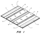
- figure 1 shows a device for applying solder to two opposite faces of a thin object such as to the stripped end portions of the conductors of a multiconductor flat cable, especially when the conductors themselves are rectangular in cross-section.
- the device comprises a support sheet 1 of a polyimide material which has a line of weakness 3 along which the sheet can be folded to define two arms 5 each having a free end 7.
- the line of weakness is U-shaped in cross-section.
- a quantity of solder in the form of a continuous strip 9 is provided on a face of each of the arms 5.
- a strip 11 of a resiliently deformable material is also provided on each of the faces of the arms 5 between the strip of solder and the respective free end. The strip 11 provides a seal between the support sheet 1 and a surface of the object on which the solder is to be provided to control flow of the solder in a direction perpendicular to the line of weakness 3.
- a coating 13 of a pressure sensitive adhesive is provided, for forming a bond between the support sheet and an object to which solder is to be applied, for locating the device on the object.
- An uncoated portion 15 of the support sheet is provided between the strip 11 of resiliently deformable material and the portion of the sheet that is coated with adhesive.
- Figure 2 shows a tool 30 for applying pressure to the device shown in Figure 1.
- the tool comprises two hinged arms 31, each having a portion 33 for applying pressure, and a cavity 35.
- the tool is positioned so that pressure is applied by the pressure applying portions 33 to the portions of the support sheet 1 that bear the strips 11 of resiliently deformable material and that no pressure is applied to the portion of the support sheet that bear solder. This ensures that flow of solder when heated is not affected by the application of pressure to the device.
- the tool may be incorporated into a heater, or may itself be arranged to provide heat to cause the solder to fuse. Otherwise, the tool together with the device and the object may be heated by an external source of heat.
- Figure 3 shows the device shown in Figure 1 positioned relative to a flat cable 21.
- the insulation has been removed from an end portion of the cable to expose the conductors 23 to which solder is to be applied.
- the support sheet 1 is folded along its line of weakness.
- the U-shape of the line of weakness 3 ensures that when the sheet is folded, the arms 5 extend from the line of weakness 3 substantially parallel to one another.
- the cable 21 is positioned within the folded support sheet 1 so that the ends of the conductors 23 abut the support sheet 1 at the line of weakness 3.
- the dimensions of the stripped portion of the cable and of the device are such that the strips 11 of resiliently deformable material contact the exposed conductors 23, and that the stripped portion of the cable extends part way along the uncoated portion 15 of the support sheet 1.
- the tool 30 is positioned around the device and the object so that the pressure applying portions 33 of the tool are positioned against the portions of the support sheet 1 that bear the strips 11 of resiliently deformable material, and so that the portions of the support sheet that bear the solder are within the cavity 35 in the tool.
- Pressure is applied to the device by means of the pressure applying portions 33 of the tool so that a seal is formed between the support sheet 1 and the conductors 23 by means of the strips 11 of resiliently deformable material.
- the seals control the flow of solder away from the ends of the conductors and, together with the folded support sleet itself, define a mold in which the solder can flow when heated.
- the assembly of the device, the cable and the tool is then heated to cause the solder 9 to fuse and to flow on the surface of the conductors 23.
Abstract
Description
- The present invention relates to a device for applying solder to one or more faces of an object, particularly to two opposite faces of an object, in a predetermined location.
- When it is desired to make a solder connection to an object, it is common first to apply a coating of solder to the object. This process is often referred to as pretinning. When the connection is to be made to the end of the object, the object may be pretinned by dipping in molten solder, for example as described in the "Soldering Manual" published by the American Welding Society May 1964 page 66. While this method of pretinning has the advantage of being quick and easily controlled, it suffers from the disadvantage that it requires that there be sufficient space around the object for a container for the molten solder. Such space is not always available. For example, the object may comprise an electrical conductor which might be fixed at one end and not be sufficiently flexible to be inserted into a container of molten solder. In another example, the conductor may be a component of a piece of electrical or electronic apparatus. During assembly or more especially during repair, it may be desirable to pretin the conductor without removing it from the apparatus. Lack of space around or within the apparatus may preclude the introduction of a container of molten solder, and furthermore, it may be desirable to introduce large quantities of molten solder into such an environment because of the possibility of loose solder forming short circuits. Yet further, particularly during repair in situ, it might not be possible to maintain a large quantity of solder in a molten space because of the lack of a suitable heat or power source.
- The present invention provides a device for applying solder to a face of an object in a predetermined location relative to an edge of the object, without the need for sufficient space around the object for a container for molten solder.
- Accordingly, in a first aspect, the invention provides a device for applying solder to a face of an object towards an edge thereof, comprising:
- (a) a support sheet having a line of weakness along which the sheet can be folded to define two arms, each having a free end;
- (b) a quantity of solder located on a face of one of the arms of the support sheet such that by folding the support sheet into a U-shape solder is applied to the surface of an object contained within the arms; and
- (c) flow control means such that flow of heated solder in a direction perpendicular to the said line of weakness is controlled.
- The device of the invention allows solder to be applied to an object in a predetermined location relative to an edge of the object by engagement of the line of weakness with the said edge. The device is particularly applicable to thin objects in which case the line of weakness allows the support sheet to be folded to adopt a U-shape, especially when the arms of the sheet extend substantially parallel away from the line of weakness. In this case, the device will be positioned with one arm of the support sheet on each side of the object.
- The device of the invention is suitable for applying solder to a flat object. It is particularly well suited to applying solder to an array of electrical conductors, especially to the stripped conductors of a multi-conductor electrical cable. Preferably, the conductors of the cable are flat conductors, by which is meant that they have a square or especially rectangular cross-section.
- Preferably, the device is provided with a quantity of solder on a face of each of the arms of the support sheet. By folding the support sheet into a U-shape, such a device may be used to apply solder to each of two opposite surfaces of an object. When the object comprises an array of conductors, surface tension effects may be relied on to provide solder on more than just the faces of the conductors that are contacted by the device. When the conductors are flat conductors that are relatively thin, for example less than 0.5 mm thick, it is possible to obtain a solder coating around the entire periphery of each conductor.
- Preferably the arrangement of the solder on the two arms of the support sheet is symmetrical so that the arrangement on one of the arms is a mirror-image of that on the other arm.
- The solder may be provided in the form of a continuous tape. Preferably the tape extends substantially parallel to the line of weakness so that the device can conveniently provide a strip of solder parallel to an edge of the object. For some applications, it can be advantageous to have the solder strip arranged at an angle to the edge of the object, in which case the solder tape will extend at an angle of between 0° and 90° to the line of weakness.
- When it is desired to provide solder on a face of an object at points which differ in distance from the edge thereof, the solder may be provided on the surface of the support sheet in an appropriate pattern of discrete quantities.
- The solder may be provided on the support sheet by lamination, this being especially preferred when the solder is provided as a continuous strip. The solder may however be provided by other techniques such as by printing. This being especially preferred when the solder is provided in a pattern of discrete quantities.
- The solder provided on the support sheet preferably includes an appropriate flux. This has the advantage that the quantity and type of flux for use in a particular application can be controlled, thereby removing the possibility of error during installation. This is not possible when tinning is achieved by dipping in a pot of molten solder when it is necessary to apply a flux as a separate operation.
- The device of the invention preferably includes a quantity of adhesive located in the same face of the support sheet as the quantity of solder between the quantity of solder and the free end of the arm on which the solder is provided. The adhesive serves to hold the device in place when it is heated to cause the solder to flow. The adhesive may also serve as the means for controlling the flow of solder in a direction perpendicular to the line of weakness in the support sheet.
- A quantity of adhesive may be provided on each of the arms of the support sheet. This enables the device to be located on the object securely. It is particularly preferred when the device is to be folded so that one arm extends along each of the opposite faces of an object, for example to provide solder on both top and bottom surfaces of an array of stripped conductors.
- The adhesive will preferably be a pressure-sensitive adhesive which allows the device of the invention to be attached temporarily to an object while solder is applied to the object, but which then allows the device to be removed. The use of such an adhesive also facilitates handling of the device prior to use since the device can be mounted on an appropriate support having a release surface, such as a sheet of release paper.
- While the adhesive, when present, may serve to control flow of solder, it is preferred to use a strip of resiliently deformable material mounted on the same face of the support sheet as the quantity of solder. The use of a resiliently deformable material ensures that the strip conforms to the surface of the object when pressure is applied in order to provide an effective seal. The dimensions of the strip will preferably be selected so that the depth of the solder applied to the object can be controlled, thereby allowing the amount of solder applied to be controlled which is important for reliable connection.
- The strip preferably extends substantially parallel to the line of weakness in the support sheet, for a preferred configuration of applied solder.
- A strip for controlling solder flow may be provided on the support sheet on one or both sides of the or each quantity of solder depending on the direction of the solder flow that is to be controlled. It is preferred that a strip is provided at least between the or each quantity of solder and the free end of the arm of the support sheet on which the solder is located. This allows flow of solder in a direction away from the line of weakness in the support sheet to be controlled. In the case of an electrical conductor to which solder is to be applied, solder is prevented from flowing along the conductor away from its free end towards insulation material which encloses the conductor.
- A strip of resilient material may also be provided between the or each quantity of solder and the line of weakness on the support sheet, in use to control flow of solder on the surface of the object towards the free end thereof. Such control may also be provided by the folded support sheet itself, since by appropriate positioning and clamping, solder can be arranged to flow along the object, towards the free end thereof, where it will encounter the fold in the support sheet. The strip of resilient material preferably comprises an elastomer such as a rubber, especially a silicone rubber.
- When the device includes a strip of resilient material in addition to a quantity of adhesive, it is preferred that there be a portion of the support sheet between the resilient material and the adhesive. This allows pressure to be applied to the resilient material to make a seal to the object while ensuring that no pressure is applied to the adhesive coated portion of the support sheet, which could lead to adhesive being left on the object when the device is removed therefrom. In some circumstances, it is important for no adhesive to be left on the object; for example when solder additional to that provided by the device is to be applied to an object it is important that the initial quantity of solder that is provided by the device is not contaminated by other materials such as an adhesive.
- For use with thin objects, the line of weakness in the support sheet is preferably such that when the sheet is folded into a U-shape, the arms extend substantially parallel from the line of weakness. Such a configuration may require appropriate clamping. The line of weakness may be provided, for example, by a U-shaped groove in the support sheet which can be considered as two sub-lines of weakness, at or towards the base of the U. A U-shaped support sheet with parallel arms has the advantage that, cooperating with a strip of resiliently deformable material when present, the support sheet is able to provide a mold in which the solder can flow on the surface of the object, and thus to control the thickness of the solder that is applied to the object.
- The support sheet may comprise a single sheet in which a line of weakness is cut or otherwise provided. To simplify manufacturing, it is preferred to use two sheets of material, each having a straight edge which is held adjacent, and substantially parallel, to the straight edge of the other sheet by a relatively flexible bridging sheet. The bridging sheet may be of the same material as the stiff sheets, and simply have a smaller thickness. The sheets may be attached to one another by means of an adhesive. In this connection, the straight edges of the sheets of stiff material, together with the sheet of flexible material, define a U-shaped groove in the support sheet.
- The support sheet may comprise several sheets that are laminated together, some of which bear solder and some of which bear a quantity of adhesive.
- The line of weakness may be provided in another manner, for example by a line of perforations or indentations.
- The material selected for the support sheet will depend on the solder material that is to be used since it is necessary that the support sheet is not affected adversely when the device is heated to cause the solder to fuse. For example, when the solder comprises 65% by weight tin and 35% by weight lead, it is preferred to use a polyimide for the support sheet.
- Preferably the distance from the line of weakness to the means for controlling the flow of solder, especially when it is provided by a strip of resiliently deformable material, is at least about 3mm, more preferably at least about 6mm; preferably the distance is less than about 15mm, more preferably less than about 10mm.
- Preferably the strip of resiliently deformable material when present stands at least about 0.2mm proud of the support sheet, more preferably from about 0.4mm to 0.6mm.
- When the solder is in the form of a tape, the width of the tape is preferably at least about 2.5mm, more preferably at least about 4mm; preferably the width is less than about 10mm, more preferably less than about 7mm. The height of the strip is preferably from about 10 to about 50 micrometers, more preferably from about 30 to about 40 micrometers.
- The invention will now be described by way of example with reference to the accompanying drawings, in which:
- Figure 1 is an isometric view of a device according to the invention prior to installation;
- Figure 2 is an isometric view of a tool for installing the device shown in Figure 1; and
- Figure 3 is a cross-section through the device shown in Figure 1 and the tool shown in Figure 2 positioned for installation on an end of a multiconductor cable.
- Referring to the drawings, figure 1 shows a device for applying solder to two opposite faces of a thin object such as to the stripped end portions of the conductors of a multiconductor flat cable, especially when the conductors themselves are rectangular in cross-section. The device comprises a support sheet 1 of a polyimide material which has a line of
weakness 3 along which the sheet can be folded to define twoarms 5 each having afree end 7. The line of weakness is U-shaped in cross-section. - A quantity of solder in the form of a
continuous strip 9 is provided on a face of each of thearms 5. Astrip 11 of a resiliently deformable material is also provided on each of the faces of thearms 5 between the strip of solder and the respective free end. Thestrip 11 provides a seal between the support sheet 1 and a surface of the object on which the solder is to be provided to control flow of the solder in a direction perpendicular to the line ofweakness 3. - At the
free end 7 of each of thearms 5, acoating 13 of a pressure sensitive adhesive is provided, for forming a bond between the support sheet and an object to which solder is to be applied, for locating the device on the object. - An
uncoated portion 15 of the support sheet is provided between thestrip 11 of resiliently deformable material and the portion of the sheet that is coated with adhesive. - Figure 2 shows a
tool 30 for applying pressure to the device shown in Figure 1. The tool comprises two hingedarms 31, each having aportion 33 for applying pressure, and acavity 35. The tool is positioned so that pressure is applied by thepressure applying portions 33 to the portions of the support sheet 1 that bear thestrips 11 of resiliently deformable material and that no pressure is applied to the portion of the support sheet that bear solder. This ensures that flow of solder when heated is not affected by the application of pressure to the device. - The tool may be incorporated into a heater, or may itself be arranged to provide heat to cause the solder to fuse. Otherwise, the tool together with the device and the object may be heated by an external source of heat.
- Figure 3 shows the device shown in Figure 1 positioned relative to a
flat cable 21. The insulation has been removed from an end portion of the cable to expose theconductors 23 to which solder is to be applied. To install the device, the support sheet 1 is folded along its line of weakness. The U-shape of the line ofweakness 3 ensures that when the sheet is folded, thearms 5 extend from the line ofweakness 3 substantially parallel to one another. Thecable 21 is positioned within the folded support sheet 1 so that the ends of theconductors 23 abut the support sheet 1 at the line ofweakness 3. The dimensions of the stripped portion of the cable and of the device are such that thestrips 11 of resiliently deformable material contact the exposedconductors 23, and that the stripped portion of the cable extends part way along theuncoated portion 15 of the support sheet 1. - The
tool 30 is positioned around the device and the object so that thepressure applying portions 33 of the tool are positioned against the portions of the support sheet 1 that bear thestrips 11 of resiliently deformable material, and so that the portions of the support sheet that bear the solder are within thecavity 35 in the tool. - Pressure is applied to the device by means of the
pressure applying portions 33 of the tool so that a seal is formed between the support sheet 1 and theconductors 23 by means of thestrips 11 of resiliently deformable material. The seals control the flow of solder away from the ends of the conductors and, together with the folded support sleet itself, define a mold in which the solder can flow when heated. - The assembly of the device, the cable and the tool is then heated to cause the
solder 9 to fuse and to flow on the surface of theconductors 23.
Claims (16)
- A device for applying solder to a face of an object towards an edge thereof, comprising:(a) a support sheet (1) having a line of weakness (3) along which the sheet can be folded to define two arms (5), each having a free end (7);(b) a quantity of solder (9) located on a face of one of the arms (5) of the support sheet (1) such that by folding the support sheet into a U-shape solder is applied to the surface of an object contained within the arms; and(c) flow control means (11) such that flow of heated solder in a direction perpendicular to the said line of weakness is controlled.
- A device as claimed in claim 1, in which a quantity of solder (9) is provided on a face of each of the arms (5) of the support sheet (1).
- A device as claimed in claim 2, in which the arrangement of the solder (9) on the two arms (5) of the support sheet (1) is symmetrical so that the arrangement on one of the arms is a mirror-image of that on the other arm.
- A device as claimed in any one of claims 1 to 3, which includes a quantity of adhesive (13) located on the same face of the support sheet (1) as the quantity of solder (9), between the quantity of solder and the free end (7) of the respective arm (5).
- A device as claimed in claim 4, in which the quantity of adhesive (13) is provided in the form of a coating on a strip-like portion of the face of the support sheet (1) at the free end (7) of the arm (5).
- A device as claimed in claim 4 or claim 5, which includes a quantity of adhesive (9) on each of the arms (5) of the support sheet (1).
- A device as claimed in any one of claims 1 to 6, in which the means (11) for controlling flow of the solder (9) comprises a strip of resiliently deformable materials mounted on the same face of the support sheet (1) as the quantity of solder.
- A device as claimed in claim 7, in which the strip of resiliently deformable material (11) extends substantially parallel to the line of weakness (3) in the support sheet (1).
- A device as claimed in claim 7 or claim 8, in which the strip of resiliently deformable material (11) is located between the quantity of solder (9) and the free end (7) of the respective arm (1).
- A device as claimed in any one of claims 1 to 9, in which the line of weakness (3) is such that when the sheet (1) is folded into a U-shape, the arms (5) extend substantially parallel from the line of weakness.
- A device as claimed in claim 10, in which the line of weakness (3) is provided by a substantially U-shaped groove in the support sheet (1).
- A device as claimed in claim 11, in which the support sheet (1) comprises two sheets of stiff material, each having a straight edge which is held adjacent, and substantially parallel, to the straight edge of the other sheet by a sheet of relatively flexible material, the straight edges of the sheets of stiff material together with the sheet of flexible material defining the U-shaped groove.
- A device as claimed in any one of claims 1 to 12, in which the line of weakness (3) is provided by a line of perforation.
- A device as claimed in any one of claims 1 to 13, in which the quantity of solder (4) is in the form of a tape.
- A device as claimed in claim 14, in which the tape extends substantially parallel to the line of weakness.
- A device as claimed in any one of claims 1 to 15, which includes flux associated with the quantity of solder (9).
Applications Claiming Priority (3)
| Application Number | Priority Date | Filing Date | Title |
|---|---|---|---|
| US07/200,998 US4807799A (en) | 1988-06-01 | 1988-06-01 | Device for applying solder |
| US200998 | 1988-06-01 | ||
| PCT/US1989/002392 WO1989011940A1 (en) | 1988-06-01 | 1989-06-01 | Device for applying solder |
Publications (2)
| Publication Number | Publication Date |
|---|---|
| EP0409906A1 EP0409906A1 (en) | 1991-01-30 |
| EP0409906B1 true EP0409906B1 (en) | 1994-05-25 |
Family
ID=22744058
Family Applications (1)
| Application Number | Title | Priority Date | Filing Date |
|---|---|---|---|
| EP89906912A Expired - Lifetime EP0409906B1 (en) | 1988-06-01 | 1989-06-01 | Device for applying solder |
Country Status (8)
| Country | Link |
|---|---|
| US (1) | US4807799A (en) |
| EP (1) | EP0409906B1 (en) |
| JP (1) | JPH03504574A (en) |
| KR (1) | KR900701458A (en) |
| AT (1) | ATE106031T1 (en) |
| CA (1) | CA1317758C (en) |
| DE (1) | DE68915543T2 (en) |
| WO (1) | WO1989011940A1 (en) |
Families Citing this family (6)
| Publication number | Priority date | Publication date | Assignee | Title |
|---|---|---|---|---|
| US5040717A (en) * | 1990-03-27 | 1991-08-20 | Metcal, Inc. | Solder delivery system |
| US5360158A (en) * | 1993-07-15 | 1994-11-01 | The S.A. Day Mfg. Co., Inc. | Method for joining aluminum alloy tubes |
| DE10084996B8 (en) * | 1999-09-20 | 2009-01-29 | Nas Interplex Industries Inc. | Solder-carrying body for use in soldering operations |
| US7754979B2 (en) * | 1999-09-20 | 2010-07-13 | Teka Interconnections Systems, Inc. | Solder-bearing wafer for use in soldering operations |
| US6900393B1 (en) * | 1999-09-20 | 2005-05-31 | Teka Interconnections Systems, Inc. | Solder-bearing wafer for use in soldering operations |
| DE102014005494A1 (en) * | 2014-03-19 | 2015-09-24 | Few Fahrzeugelektrikwerk Gmbh & Co. Kg | Method and device for uniform coating of a metallic or metallized industrial hose |
Family Cites Families (7)
| Publication number | Priority date | Publication date | Assignee | Title |
|---|---|---|---|---|
| DE2018810A1 (en) * | 1970-04-20 | 1971-11-04 | Rau Fa G | Soldering template and manufacturing process for this |
| SU625890A1 (en) * | 1977-04-15 | 1978-09-30 | Киевский Ордена Ленина Политехнический Институт Им.50-Летия Великой Октябрьской Социалистической Революции | Welding clamp |
| SU698741A1 (en) * | 1978-01-16 | 1979-11-25 | Киевский Ордена Ленина Политехнический Институт Им.50-Летия Великой Октябрьской Социалистической Революции | Hold-down device for welding thin-sheet articles |
| GB2113134B (en) * | 1981-12-08 | 1986-01-15 | Raychem Corp | Device for connecting electrical conductors |
| SU1021544A1 (en) * | 1982-01-21 | 1983-06-07 | Научно-Производственное Объединение По Технологии Машиностроения "Цниитмаш" | Method of manufacturing specimen for investigating welding connection properties |
| JPS61985A (en) * | 1984-06-12 | 1986-01-06 | Nec Corp | Microfloppy disc device |
| US4728022A (en) * | 1986-09-19 | 1988-03-01 | Hughes Aircraft Company | Mask and solder form |
-
1988
- 1988-06-01 US US07/200,998 patent/US4807799A/en not_active Expired - Fee Related
-
1989
- 1989-06-01 EP EP89906912A patent/EP0409906B1/en not_active Expired - Lifetime
- 1989-06-01 DE DE68915543T patent/DE68915543T2/en not_active Expired - Fee Related
- 1989-06-01 JP JP1506498A patent/JPH03504574A/en active Pending
- 1989-06-01 WO PCT/US1989/002392 patent/WO1989011940A1/en active IP Right Grant
- 1989-06-01 AT AT89906912T patent/ATE106031T1/en not_active IP Right Cessation
- 1989-06-01 CA CA000601431A patent/CA1317758C/en not_active Expired - Fee Related
-
1990
- 1990-02-01 KR KR1019900700207A patent/KR900701458A/en not_active Application Discontinuation
Also Published As
| Publication number | Publication date |
|---|---|
| KR900701458A (en) | 1990-12-03 |
| CA1317758C (en) | 1993-05-18 |
| EP0409906A1 (en) | 1991-01-30 |
| DE68915543D1 (en) | 1994-06-30 |
| DE68915543T2 (en) | 1995-01-05 |
| US4807799A (en) | 1989-02-28 |
| JPH03504574A (en) | 1991-10-09 |
| WO1989011940A1 (en) | 1989-12-14 |
| ATE106031T1 (en) | 1994-06-15 |
Similar Documents
| Publication | Publication Date | Title |
|---|---|---|
| US4489487A (en) | Electronic component and adhesive strip combination, and method of attachment of component to a substrate | |
| US3964666A (en) | Bonding contact members to circuit boards | |
| US4775917A (en) | Thermal compensated circuit board interconnect apparatus and method of forming the same | |
| US4541034A (en) | Electrical terminal and method of securing same in circuit substrate thru-hole | |
| CA1067613A (en) | Hermetically sealed film resistor | |
| EP0160345A2 (en) | Pre-patterned device substrate device-attach adhesive transfer system | |
| JPS6243784B2 (en) | ||
| EP0206619A2 (en) | Self-soldering, flexible circuit connector | |
| EP0409906B1 (en) | Device for applying solder | |
| EP0303873B1 (en) | Conductive lead arrangement | |
| US5198391A (en) | Method for bonding llccc-components using a leadframe | |
| EP0250045A1 (en) | Method of mounting refined contact surfaces on a substrate and substrate provided with such contact surfaces | |
| CA1179837A (en) | Method for constructing an electrical interconnection circuit and apparatus for realising the method | |
| JP3948680B2 (en) | Method of providing metal terminals for surface mountable electrical components and electrical components | |
| US4728022A (en) | Mask and solder form | |
| FI93911C (en) | A pin that is attached to the circuit board by soldering | |
| JP4188831B2 (en) | Replaceable surface mount element clip | |
| GB2113134A (en) | Device for connecting electrical conductors | |
| EP1147573B1 (en) | Collapsible electrical leads for engaging a substrate | |
| JP2001291541A (en) | Structure and method for connecting flat wire harness | |
| EP0611064B1 (en) | Solder pad configuration for wave soldering | |
| GB2392862A (en) | Soldering and repair of flat wires | |
| JPH07111897B2 (en) | Method of connecting electrode formed on conductive film and lead wire | |
| JPH08203577A (en) | Connection of flat cable and printed wiring board | |
| JPH0365670B2 (en) |
Legal Events
| Date | Code | Title | Description |
|---|---|---|---|
| PUAI | Public reference made under article 153(3) epc to a published international application that has entered the european phase |
Free format text: ORIGINAL CODE: 0009012 |
|
| 17P | Request for examination filed |
Effective date: 19901115 |
|
| AK | Designated contracting states |
Kind code of ref document: A1 Designated state(s): AT BE CH DE FR GB IT LI NL SE |
|
| 17Q | First examination report despatched |
Effective date: 19920812 |
|
| GRAA | (expected) grant |
Free format text: ORIGINAL CODE: 0009210 |
|
| AK | Designated contracting states |
Kind code of ref document: B1 Designated state(s): AT BE CH DE FR GB IT LI NL SE |
|
| PG25 | Lapsed in a contracting state [announced via postgrant information from national office to epo] |
Ref country code: IT Free format text: LAPSE BECAUSE OF FAILURE TO SUBMIT A TRANSLATION OF THE DESCRIPTION OR TO PAY THE FEE WITHIN THE PRE;WARNING: LAPSES OF ITALIAN PATENTS WITH EFFECTIVE DATE BEFORE 2007 MAY HAVE OCCURRED AT ANY TIME BEFORE 2007. THE CORRECT EFFECTIVE DATE MAY BE DIFFERENT FROM THE ONE RECORDED.SCRIBED TIME-LIMIT Effective date: 19940525 Ref country code: CH Effective date: 19940525 Ref country code: NL Effective date: 19940525 Ref country code: BE Effective date: 19940525 Ref country code: LI Effective date: 19940525 Ref country code: AT Effective date: 19940525 Ref country code: SE Free format text: THE PATENT HAS BEEN ANNULLED BY A DECISION OF A NATIONAL AUTHORITY Effective date: 19940525 |
|
| REF | Corresponds to: |
Ref document number: 106031 Country of ref document: AT Date of ref document: 19940615 Kind code of ref document: T |
|
| REF | Corresponds to: |
Ref document number: 68915543 Country of ref document: DE Date of ref document: 19940630 |
|
| ET | Fr: translation filed | ||
| REG | Reference to a national code |
Ref country code: CH Ref legal event code: PL |
|
| NLV1 | Nl: lapsed or annulled due to failure to fulfill the requirements of art. 29p and 29m of the patents act | ||
| PLBE | No opposition filed within time limit |
Free format text: ORIGINAL CODE: 0009261 |
|
| STAA | Information on the status of an ep patent application or granted ep patent |
Free format text: STATUS: NO OPPOSITION FILED WITHIN TIME LIMIT |
|
| 26N | No opposition filed | ||
| PGFP | Annual fee paid to national office [announced via postgrant information from national office to epo] |
Ref country code: GB Payment date: 19970523 Year of fee payment: 9 |
|
| PGFP | Annual fee paid to national office [announced via postgrant information from national office to epo] |
Ref country code: DE Payment date: 19970606 Year of fee payment: 9 |
|
| PGFP | Annual fee paid to national office [announced via postgrant information from national office to epo] |
Ref country code: FR Payment date: 19970610 Year of fee payment: 9 |
|
| PG25 | Lapsed in a contracting state [announced via postgrant information from national office to epo] |
Ref country code: GB Free format text: LAPSE BECAUSE OF NON-PAYMENT OF DUE FEES Effective date: 19980601 |
|
| GBPC | Gb: european patent ceased through non-payment of renewal fee |
Effective date: 19980601 |
|
| PG25 | Lapsed in a contracting state [announced via postgrant information from national office to epo] |
Ref country code: FR Free format text: LAPSE BECAUSE OF NON-PAYMENT OF DUE FEES Effective date: 19990226 |
|
| PG25 | Lapsed in a contracting state [announced via postgrant information from national office to epo] |
Ref country code: DE Free format text: LAPSE BECAUSE OF NON-PAYMENT OF DUE FEES Effective date: 19990401 |
|
| REG | Reference to a national code |
Ref country code: FR Ref legal event code: ST |