EP0408534A2 - Phasengeschalteter Leistungsregler - Google Patents
Phasengeschalteter Leistungsregler Download PDFInfo
- Publication number
- EP0408534A2 EP0408534A2 EP90850269A EP90850269A EP0408534A2 EP 0408534 A2 EP0408534 A2 EP 0408534A2 EP 90850269 A EP90850269 A EP 90850269A EP 90850269 A EP90850269 A EP 90850269A EP 0408534 A2 EP0408534 A2 EP 0408534A2
- Authority
- EP
- European Patent Office
- Prior art keywords
- power controller
- full wave
- output
- source
- power
- Prior art date
- Legal status (The legal status is an assumption and is not a legal conclusion. Google has not performed a legal analysis and makes no representation as to the accuracy of the status listed.)
- Withdrawn
Links
Images


Classifications
-
- H—ELECTRICITY
- H02—GENERATION; CONVERSION OR DISTRIBUTION OF ELECTRIC POWER
- H02M—APPARATUS FOR CONVERSION BETWEEN AC AND AC, BETWEEN AC AND DC, OR BETWEEN DC AND DC, AND FOR USE WITH MAINS OR SIMILAR POWER SUPPLY SYSTEMS; CONVERSION OF DC OR AC INPUT POWER INTO SURGE OUTPUT POWER; CONTROL OR REGULATION THEREOF
- H02M5/00—Conversion of AC power input into AC power output, e.g. for change of voltage, for change of frequency, for change of number of phases
- H02M5/02—Conversion of AC power input into AC power output, e.g. for change of voltage, for change of frequency, for change of number of phases without intermediate conversion into DC
- H02M5/04—Conversion of AC power input into AC power output, e.g. for change of voltage, for change of frequency, for change of number of phases without intermediate conversion into DC by static converters
- H02M5/22—Conversion of AC power input into AC power output, e.g. for change of voltage, for change of frequency, for change of number of phases without intermediate conversion into DC by static converters using discharge tubes with control electrode or semiconductor devices with control electrode
- H02M5/25—Conversion of AC power input into AC power output, e.g. for change of voltage, for change of frequency, for change of number of phases without intermediate conversion into DC by static converters using discharge tubes with control electrode or semiconductor devices with control electrode using devices of a thyratron or thyristor type requiring extinguishing means
- H02M5/257—Conversion of AC power input into AC power output, e.g. for change of voltage, for change of frequency, for change of number of phases without intermediate conversion into DC by static converters using discharge tubes with control electrode or semiconductor devices with control electrode using devices of a thyratron or thyristor type requiring extinguishing means using semiconductor devices only
- H02M5/2573—Conversion of AC power input into AC power output, e.g. for change of voltage, for change of frequency, for change of number of phases without intermediate conversion into DC by static converters using discharge tubes with control electrode or semiconductor devices with control electrode using devices of a thyratron or thyristor type requiring extinguishing means using semiconductor devices only with control circuit
-
- G—PHYSICS
- G05—CONTROLLING; REGULATING
- G05F—SYSTEMS FOR REGULATING ELECTRIC OR MAGNETIC VARIABLES
- G05F1/00—Automatic systems in which deviations of an electric quantity from one or more predetermined values are detected at the output of the system and fed back to a device within the system to restore the detected quantity to its predetermined value or values, i.e. retroactive systems
- G05F1/10—Regulating voltage or current
- G05F1/12—Regulating voltage or current wherein the variable actually regulated by the final control device is AC
- G05F1/40—Regulating voltage or current wherein the variable actually regulated by the final control device is AC using discharge tubes or semiconductor devices as final control devices
- G05F1/44—Regulating voltage or current wherein the variable actually regulated by the final control device is AC using discharge tubes or semiconductor devices as final control devices semiconductor devices only
- G05F1/45—Regulating voltage or current wherein the variable actually regulated by the final control device is AC using discharge tubes or semiconductor devices as final control devices semiconductor devices only being controlled rectifiers in series with the load
- G05F1/455—Regulating voltage or current wherein the variable actually regulated by the final control device is AC using discharge tubes or semiconductor devices as final control devices semiconductor devices only being controlled rectifiers in series with the load with phase control
-
- H—ELECTRICITY
- H05—ELECTRIC TECHNIQUES NOT OTHERWISE PROVIDED FOR
- H05B—ELECTRIC HEATING; ELECTRIC LIGHT SOURCES NOT OTHERWISE PROVIDED FOR; CIRCUIT ARRANGEMENTS FOR ELECTRIC LIGHT SOURCES, IN GENERAL
- H05B41/00—Circuit arrangements or apparatus for igniting or operating discharge lamps
- H05B41/14—Circuit arrangements
- H05B41/36—Controlling
- H05B41/38—Controlling the intensity of light
- H05B41/39—Controlling the intensity of light continuously
- H05B41/392—Controlling the intensity of light continuously using semiconductor devices, e.g. thyristor
- H05B41/3921—Controlling the intensity of light continuously using semiconductor devices, e.g. thyristor with possibility of light intensity variations
- H05B41/3924—Controlling the intensity of light continuously using semiconductor devices, e.g. thyristor with possibility of light intensity variations by phase control, e.g. using a triac
Definitions
- This invention relates to the field of AC power controllers and in particular to a phase-triggered control operable to apply power to a load during a controllable portion of each power half-cycle.
- the objective is the same in each case, namely to determine by preferably-variable means the precise point at which the triac will be turned on, applying current to the load at substantially the full supply voltage until the next zero crossing when, unless again triggered, the change in voltage polarity will turn the triac off.
- “on” and “off” denote the conducting and non-conducting states of the triac, respectively.
- the Tolmie reference employs two comparators, one for sensing the point of zero crossing on the supply voltage, and the other adjustably determining the phase delay until triggering of the triac.
- a series regulated power supply is provided to obtain a fixed DC voltage to power the comparators, i.e., high gain operational amplifiers. This accurate voltage supply is also used to provide an accurate voltage reference for detecting zero crossings in a full wave rectified signal derived form the power line.
- Coats et al discloses a controller which can be operated by computer outputs and the like, using timing elements including unijunction and field-effect transistors.
- the objective is detecting zero crossings in the supply power, and timing the interval to a point at which a triac will be turned on.
- Coats' controller like Tolmie's controller, is a complicated and expensive device which requires precise DC voltage regulation for its respective elements.
- a series of zener diodes are provided for accurately regulating the supply voltage to the timing elements.
- a series regulator is used in Tolmie.
- Precise DC voltage control is normally considered necessary for supplying integrated circuit timers, unijunction transistor timers and the like. Without good supply voltage regulation, accurate results are normally expected. Supply voltage is typically regulated using a series power transistor with a zener diode reference, directly or indirectly controlling the conductance of the series transistor. In addition to the cost of these components, a good series regulator generates some overhead in terms of heat sinks and the like, which would be avoided if there were routinely possible.
- the result of the control is that the RMS power applied to the load is adjustable, while the peak voltage of the supply is not reduced in the power applied to the load. This renders the control especially applicable for adjusting lighting systems, for example with fluorescent bulbs, wherein it is desirable that the supply voltage reach the peak voltage, at least for a time during a half cycle.
- a power control for an incandescent lamp is disclosed in U.S. Patent No. 4,549,116-Andrews. Thyristor controls with triacs or SCRs are also useful in connection with other types of devices, for example, electric motors.
- An SCR-triggered control is U.S. Patent No. 3,447,057-Brown et al.
- thyristor controls can be used at frequencies or voltage levels other than that of the conventional utility or generation driven power lines.
- U.S. Patent No. 4,623,824-Scolari et al discloses an SCR-switched power control for a DC/AC inverter and voltage multiplier.
- a comparator senses zero crossings by comparing a fully wave rectified periodic signal with a low-pass filtered full wave rectified signal, the comparator also being powered by this filtered signal, notwithstanding the lack of series regulation.
- Timers having RC timing elements adjustably determine the phase delay and provide a pulse for triggering the triac during each half cycle.
- the timers are also powered by the filtered full wave rectified signal.
- a recision potentiometer is employed in the RC network for the timer determining the phase delay. This potentiometer may be a multi-turn pot with a numeric indicator for precise control.
- the apparatus is especially applicable to fluorescent lighting control and can be packaged as a unit operable to control one or more circuits.
- phase switched power controller which connects a load to an alternating current source for a controllable proportion of each half cycle, as selected by the user.
- a first full wave rectifier is connected to the voltage source and produces an output signal varying between zero and a predetermined peak.
- a low pass filtered full wave rectified signal is preferably obtained from a second full wave rectifier and a controllable DC reference voltage is obtained therefrom.
- the output of the first rectifier and the reference voltage are input into a voltage comparator, the output of which triggers a triac which connects the load to the power source during a predetermined portion of the cycle beginning or ending at a time defined by the output of the comparator.
- one embodiment of the invention includes a timing circuit for generating a timed override signal which triggers the triac for all of the cycles of the power supply. When the override signal is removed, the triac fires dependent upon the output of the comparator.
- Fig. 1 is a schematic illustration of a power controller according to the invention. Alternating current power along supply lines 22 is to be applied to load 24 during an adjustable portion of each half cycle on the power lines 22. This is accomplished by timing the triggering of a thyristor, for example, triac 70, which is in series with load 24 and connected across the AC supply lines 22. A bypass switch 26 is connected in parallel with triac 70, such that full power can be applied to load 24 when desired, bridging the control means.
- a thyristor for example, triac 70
- Transformer 28 steps down the voltage supplied on lines 22 to levels appropriate for integrated circuit components, for example, 5 to 12 volts, etc.
- the voltage on the supply side at lines 22 can be any appropriate voltage for load 24, for example 110, 220, 477 (for lighting circuits), or the like.
- the frequency of the power can vary, for example, 50, 60 or 440 hertz.
- a convenient switch or jumper panel is provided to enable the installer to connect the supply side of the transformer 28 to any of the standard supply voltages, the transformer having windings form 120, 240 or 480 VAC, for example. Other available voltages and frequencies can be used as well.
- transformer 28 The voltage level on either side of transformer 28 is a sine wave, as shown in Fig. 2.
- a full wave rectifier 32 converts the sine wave voltage into a full wave rectified voltage, as shown in Fig. 3.
- Rectifier 32 is provided by diodes 34, one or the other of which conducts during positive and negative excursions of the power, respectively.
- Transformer 28 can be a center-tapped transformer on the secondary side.
- Comparator 60 is a high gain operational amplifier. Whenever the voltage at the non-inverting input exceeds the voltage at the inverting input, the output of comparator 60 will be high. When the voltage at the inverting input exceeds the voltage at the non-inverting input, then the comparator output will change state. Comparator 60 is powered by a full wave rectified and filtered voltage, for example, the filtered output 42 of a full wave bridge rectifier 40, generally designated as "+V".
- a low pass filter 50 is defined by parallel storage capacitor 52, together with the series resistance of the diodes in the bridge rectifier 40.
- An additional series resistor can be included if desired between bridge rectifier 40 and DC voltage supply 42 to lower the low pass frequency.
- the DC voltage at point 42 designated as "IV" is substantially a DC signal, but also has substantial ripple, as shown in Fig. 4, due to the lack of a series regulator.
- the voltage at the input to the comparator is reduced substantially by series resistance 56, but still has a good bit of ripple. Nevertheless, whenever the full wave rectified signal (Fig. 3) crosses the reduced supply voltage (Fig. 4) used as a reference input, the output of comparator 60 will change state, i.e., during every half cycle.
- Resistor 56 setting the level of the second input to comparator 60, is large enough that the DC level at the input to the comparator is very low, for example, 0.8-1.0 V or just low enough to accommodate the forward biased voltage drop across diodes 34. IN this manner, comparator 60 will reduce a square wave pulse substantially corresponding to the zero crossings in the AC signal.
- Timer 82 is a standard integrated circuit timer, for example one of two timers on dual timer model NE556, marketed by Texas Instruments. When triggered, the timer 82 produces a pulse output whose width is determined by an RC network connected thereto.
- Capacitor 84 and potentiometer 86 are connected to the timing inputs to timer 82, whereby adjusting potentiometer sets the pulse length of the output of timer 82. The values of capacitor 84 and resistor 86 are set such that timer 82 will time out at a selected point following the zero crossing as detected by comparator 60.
- timer 82 The output of timer 82 is differentiated by series capacitor 92, i.e., the low going transistor on the output of timer 82 produces a low going pulse on the input to timer 112.
- the normal level of the input at timer 112 is pulled up by resistor 94 such that the input to timer 112 is normally high, but a low going pulse occurs when timer 82 times out.
- Timer 112 is then triggered.
- Timer 112 has a shorter pulse width, determined by an RC network 114 thereon.
- the output of timer 112 is a high going pulse which causes drive transistor 116 to conduct, thereby placing a pulse on gate 72 to triac 70 and causing the triac to begin conducting.
- Triac 70 continues to conduct until the next zero crossing, apply to load 24 a voltage substantially equal to the voltage across lines 22 on the AC supply.
- a further timer 132 can be provided, having an integrating input rather than a differentiating input as does timer 112.
- the input RC network to timer 132 will further delay the output pulse to the associated drive transistor 116.
- the delay will be equal to the time required for the input to timer 132 to rise above its logical threshold, as the parallel capacitor on the input charges through the series resistor.
- the power applied to load 24 will be substantially as shown in Fig. 5.
- a delay during which the voltage is zero occurs after each zero crossing, until triac 70 is triggered via a pulse from timer 112, occurring at a time defined by timer 82. Accordingly, the peak voltage is equal to the peak voltage at the input, but the RMS value of the power supply to lead 24 is less than would be available if the power control was bypassed, for example, by switch 26.
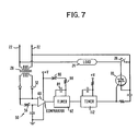
- FIG. 7 A simplified alternative embodiment of the invention is shown in Fig. 7. This embodiment is similar to that of Fig. 1, however, the same full wave rectifier 32 is used to produce both inputs to comparator 60.
- One input is connected to the raw full wave rectified output from rectifier 32 and the other is connected thereto through a low pass filter 50, including a series resistor and parallel capacitor.
- the series resistor 56 applied to the second input to comparator 60 is variable, thereby allowing the user to adjust the level at which comparator 60 will be triggered.
- This is another method of adjusting the phase delay, and results in comparator 60 changing state earlier or later after the zero crossing on the AC power line as defined by the full wave rectified signal crossing the set threshold. Accordingly, comparator 60 will be sensitive to a voltage occurring somewhere between the maximum and minimum of the full wave rectified signal. Should the comparator 60 be arranged to trigger at a later point after a zero crossing, then the time value for timer 82 can be reduced accordingly.
- timer 82 is provided with a timing network including a capacitor and two resistors through which the capacitor is charged to determine the pulse width of the timer.
- a fixed resistor 90 together with a variable resistor 86 is provided.
- Fixed resistor 90 can be of an appropriate value together with the timing capacitor 84 such that when variable resistor 86 is zero, the delay between triggering of timer 82 and timing out of timer 82 is exactly long enough to coincide with the next successive zero crossing.
- comparator 60 senses a zero crossing (or other threshold level) during one half cycle, and uses this to trigger a pulse from timer 112 during a next or succeeding one of the half cycles.
- Potentiometer 86 may be a precision multi-turn potentiometer, as shown in Fig. 6.
- a numeric indicator 88 is provided. The user can precisely set the desired level using the precision potentiometer.
- the resistance of potentiometer 86 is arranged such that over its span from 00 to 999, the resulting delay varies from 0 to a complete half cycle on the power line.
- Fig. 8 illustrates specific preferred circuit design according to the invention, including specific component identifications.
- the components are arranged to show which are included on the same circuit card and which are external to the circuit card, packaged in the unit.
- Switch 160 is provided for changing the windings on transformer 28 to accommodate different voltage levels, for example, 120 or 240 volts AC.
- Red and green LED indicators 162, 164 reflect the output of the pulse timers, and the extent of their illumination generally reflects the proportionate power control setting at the time.
- a fuse 166 is preferably included on the supply side of transformer 28, for safety purposes.
- a lamp 168 can be provided on show the "on" state of the incoming power, or to likewise reflect application of power to the load 24, lamp 168 being in that case connected parallel to load 24.
- the elements external to the printed circuit card are placed externally such that they will be accessible or visible on an external housing, or with respect to triac 70, so that the triac can be mounted to a heat sink.
- the other elements of the circuit do not dissipate a great deal of current, and stay moderately cool during operation.
- the apparatus is preferably mounted in a heavy duty junction box of the same type used for circuit breakers at the service supply panel.
- This junction box can be immediately associated with a breaker box (e.g., mounted next to it) and wired such that circuits in the establishment leading to the lighting equipment are controlled by the apparatus.
- the housing can be an indoor/outdoor enclosure, sealed such that dirt, dust, oil, rain, moisture and dripping water are excluded.
- the variable electronic control of the invention power consumption of the lighting circuits is reduced for lighting loads.
- the electronic control is especially useful for fluorescent lighting, including lamps and ballasts for mercury and metal halide lamps, high or low pressure sodium lamps, other fluorescent lamps, mercury vapor lamps, etc.
- the apparatus is preferably configured to control a number of such lamps.
- the preferred commercial models, for example, are configured for 120/240/480 volts AC, and 50 or 100 Amps (46 KW or 96 KW).
- the invention which includes many such modifications and improvements, is characterized as a power controller operable to connect a load 24 to a source 22 of periodically varying electric power for a user-selected interval during each cycle thereof.
- the power controller has at least one full wave rectifier 32, 40 connectable to power from the source 22, 28, the full wave rectifier 34 producing an unfiltered output signal "III" varying between zero and a predetermined peak.
- a low pass filter 50 is connected to the at least one full wave rectifier 32.
- the low pass filter is connected to the at least one full wave rectifier 34, the low pass filter 50 having an output voltage "IV" substantially equal to a predetermined DC voltage, the output signal of the full wave rectifier 32 varying periodically to cross said DC voltage at regular times during each cycle of the periodically varying power.
- a comparator 60 is operable to compare the unfiltered output signal III and the output voltage IV of the low pass filter 50, to sense said regular times.
- Switch means 70 are responsive to an output of comparator 60, the switch means 70 connecting the source 22 and the load 24 during a predetermined portion of the cycle beginning or ending at a time defined by the output of the comparator 60. Means 86, 82 are included for varying one of the beginning and the ending.
- a timer 82 is preferably responsive to the output of the comparator 60, whereby one of the beginning and ending is defined by the timer 82 timing out, the other of the beginning and the ending is defined by a zero crossing on the AC signal.
- the switch means preferably comprises a thyristor 70, whereby the switch means once triggered remains operable to connect the source 22 to the load 24 until a reversal of polarity of the electric power.
- Timer 82 preferably begins timing at a reversal of polarity (i.e., a zero crossing) of the electric power and the switch means 70 is triggered when the timer 82 times out.
- the means for varying one of the beginning and ending of the triggering cycle preferably includes a manually variable potentiometer 86, which can be connected in an RC circuit 84, 86 at an input to the timer 82 defining a timer interval length between zero crossing and a triggering of the switch means 70,
- a potentiometer may be connected to an input to the comparator 60, for adjusting a relative proportion of one of the unfiltered output of the full wave rectifier and the output signal of the low pass filter, thereby adjusting the initiation of timing by a timer 82.
- the potentiometer is a multi-turn precision potentiometer, including a numerical digital indicator 88.
- the timer interval can be greater than an interval of a half cycle of the source, whereby the timer is triggered in a first half cycle and times out in a later half cycle.
- the device is applicable to power sources of alternating current electric power, for example at standard frequencies of 50, 60 and 440 hertz.
- the source may be alternating current domestic electric power at one of 110, 220, 440 volts AC (120/240/480), or at other power levels.
- the device is mounted in a housing and additional power controllers may be included in the housing for controlling additional loads. In this connection, the power controllers may control loads at different voltages.
- Fig. 11 is a schematic showing another embodiment of the invention.
- the 120 or 240 volt AC power supply is connected to step down transformer 310. Coupled across AC power supply is load 312. This configuration is similar to that shown in Fig. 1.
- Transformer 310 is a step down transformer and further isolates the AC power supply to the balance of the controller circuit.
- the transformer output is fed to a full wave rectifier configured as diodes 314 and 316. This full wave rectifier rectifies the step down, AC signal to a signal similar to that shown in Fig. 12 and identified in Fig. 11 by A.
- the signal is then applied to a filter consisting of resistors 318 and 320 and a capacitor 322. Resistors 318 and 320 act in part as a voltage divider network.
- resistors 318 and 320 and capacitor 322 are configured as a high pass filter for signal A (Fig. 12).
- This modified signal is fed to input 324 of comparator 326.
- the output of comparator 326 is generally represented by signal B, as shown in Fig. 13.
- the comparator fires when signal A (Fig. 12) reaches a controllable DC reference voltage identified as level D in Fig. 12.
- Controllable DC reference voltage is applied to input 328 of comparator 326.
- the output of the comparator is fed to an RC filter configured as capacitor 330 and resistor 332.
- Resistor 334 is used to feed back certain voltage into comparator 326 based upon the manufacturer's specification for the integrated circuit containing the comparator.
- the output of the RC filter consisting of capacitor 330 and resistor 332 is fed to the base of a transistor switch 340.
- signal B shown in Fig. 13 would be affected by the RC filter, capacitor 330 and resistor 332 and the signal would change based upon the charging and discharging of capacitor 330.
- the output of comparator 326 drives transistor 340 which in turn makes transistor 340 conduct to fire triac 350 connected to the circuit via resistor 352.
- Resistor 352 simply sets the voltage level for the gate on the triac.
- the circuit includes a full wave bridge rectifier 360 connected on one side to transformer 310 and connected to a low pass filter consisting of capacitor 362 and the resistance present in the diodes comprising bridge rectifier 360.
- the low pass filter (a portion of bridge rectifier 360 and capacitor 362) is fed through a resistor 364 to a variable resistor 366.
- the other end of variable resistor 366 is coupled to a further variable resistor 368 and ultimately to ground.
- the controllable output line of resistor 366 that is line 370, carries the controllable DC reference voltage to comparator 326. Accordingly, the level of the controllable DC reference voltage is set by the position of variable resistor 366.
- Variable resistor 366 is comparable to the potentiometers which set the firing of the comparators in Figs. 1 and 7.
- the resistance in bridge rectifier 360 and capacitor 362 in combination with variable resistor 366 is a low pass filter means which generates the controllable DC reference voltage.
- the switch means, triac 350, is responsive to the output of comparator 326.
- variable resistor 366 can be set based upon the particular load attached to the controller and to the power supply line. For example, based upon previous testing of fluorescent ballast lighting circuits, it is known that it takes about two minutes for the load to reach a stable power consumption level. This occurs due to the heating of the internal elements. In another instance, a high intensity discharge lamp may take up to 20 minutes to reach a stable power consumption level. Variable resistor 366 may be set by the operator dependent upon the type of load coupled to the AC power source and dependent upon the data gathered for that particular type of load.
- variable resistor 366 may wish to set the position of variable resistor 366 and, hence, control the level of the DC reference voltage applied on line 370 and fed to comparator 326.
- a load set circuit 400 that generates a timed override signal which essentially is applied to triac 350 such that the triac is closed during all of the cycle of the Ac power supply.
- Fig. 15 is a schematic illustrating load set circuit 40.
- the load set circuit can be removably coupled or decoupled from the balance of the circuit via jacks 412 and 414.
- jacks 412 and 414 Of course, it is not necessary to include these jacks since, as will be explained later, the load set circuit generates an override signal only during the initial start up of the device. Switches can replace jacks 414 and 412 such that the operator could switch out the load set circuit after variable resistor 366 has been set for maximum power savings.
- the load set circuit illustrated in Fig. 15 includes a low pass filter 418, consisting of resistor 420 and diode 422 and capacitor 424.
- the low pass filter 418 is preferably configured as a ripple filter and is connected to input line 426 that is ultimately connected to bridge rectifier 360 and capacitor 362, that is, the second full wave rectifier and the low pass filter in Fig. 11.
- the output of low pass filter 414 is carried by line 430 to the input of timer 432.
- the power supplied to timer 432 by lines 434 and also that power signal is applied to the reset pin 436 of timer 432.
- timer 432 is a monostable, multi-vibrator (MMV) which is generally designated as an integrated circuit number 555(A) or (E).
- MMV monostable, multi-vibrator
- Timer 432 generates the timed override signal on line 438.
- the timed override signal is shown in Fig. 14.
- Resistor 440 simply sets the voltage level for the gate of transistor 442.
- transistor 442 is activated and the override signal C shown in Fig. 14 is applied to jack 414, resistor 352 (Fig. 11 and ultimately to the gate of triac 350.
- the MMV timer 432 has a pulse which is set by pulse set circuit 460 as well as capacitor 462.
- pulse set circuit 460 is a single resistor which, in combination with capacitor 462, establishes an RC network which is a time delay which in turn establishes the width of the pulse at output line 438 and hence the activation of transistor 442 and the pulse width of override signal C as shown in Fig. 14.
- pulse set circuit 460 can be a variable resistor or a bank of resistors which are switched in such that different pulse widths are obtained varying, for example, between one minute up to 20 minutes.
- the load set circuit In operation, the load set circuit generates a timed override signal and applies that signal to the gate of triac 350.
- triac 350 In the absence of the timed override signal, triac 350 is solely responsive to comparator 326, that is, the triac is fired during a predetermined portion of the cycle of the AC power supply beginning or ending at a time defined by the output of the comparator. Since the MMV timer 432 has the power connected to reset input 436, the timer only fires when the power is initially applied to the controller circuit. Accordingly, timer 432 is a time out circuit that is activated by the presence of a first output of the low pass filter consisting of bridge rectifier 360 and capacitor 362.
Landscapes
- Engineering & Computer Science (AREA)
- Power Engineering (AREA)
- Physics & Mathematics (AREA)
- Electromagnetism (AREA)
- General Physics & Mathematics (AREA)
- Radar, Positioning & Navigation (AREA)
- Automation & Control Theory (AREA)
- Rectifiers (AREA)
- Control Of Electrical Variables (AREA)
Applications Claiming Priority (4)
| Application Number | Priority Date | Filing Date | Title |
|---|---|---|---|
| US07/378,855 US4935691A (en) | 1989-07-12 | 1989-07-12 | Phase switched power controller |
| US53826190A | 1990-06-14 | 1990-06-14 | |
| US538261 | 1990-06-14 | ||
| US378855 | 1995-01-25 |
Publications (2)
| Publication Number | Publication Date |
|---|---|
| EP0408534A2 true EP0408534A2 (de) | 1991-01-16 |
| EP0408534A3 EP0408534A3 (en) | 1991-04-10 |
Family
ID=27008373
Family Applications (1)
| Application Number | Title | Priority Date | Filing Date |
|---|---|---|---|
| EP19900850269 Withdrawn EP0408534A3 (en) | 1989-07-12 | 1990-07-11 | Phase switched power controller |
Country Status (1)
| Country | Link |
|---|---|
| EP (1) | EP0408534A3 (de) |
Cited By (3)
| Publication number | Priority date | Publication date | Assignee | Title |
|---|---|---|---|---|
| EP0516008A3 (en) * | 1991-05-29 | 1993-01-07 | Abb Patent Gmbh | Electrical apparatus for continuous load regulation |
| EP2104401A1 (de) | 2008-03-17 | 2009-09-23 | Universal Lighting Technologies, Inc. | Nulldurchgangserkennung von Leitungsspannung/-strom unterschiedlicher Amplitude |
| CN110926037A (zh) * | 2019-12-12 | 2020-03-27 | 中山市上航电子有限公司 | 兼容emc的大功率水器的调压控制方法 |
Family Cites Families (3)
| Publication number | Priority date | Publication date | Assignee | Title |
|---|---|---|---|---|
| US3447057A (en) * | 1966-07-14 | 1969-05-27 | Cutler Hammer Inc | Solid state power controller for a.c. load devices |
| GB1323441A (en) * | 1969-06-20 | 1973-07-18 | Matsushita Electric Industrial Co Ltd | Converter for changing alternating current into direct current |
| US4506177A (en) * | 1982-12-06 | 1985-03-19 | Raab Herman P | Function generator with means for selectively changing the discharge time constant |
-
1990
- 1990-07-11 EP EP19900850269 patent/EP0408534A3/en not_active Withdrawn
Cited By (3)
| Publication number | Priority date | Publication date | Assignee | Title |
|---|---|---|---|---|
| EP0516008A3 (en) * | 1991-05-29 | 1993-01-07 | Abb Patent Gmbh | Electrical apparatus for continuous load regulation |
| EP2104401A1 (de) | 2008-03-17 | 2009-09-23 | Universal Lighting Technologies, Inc. | Nulldurchgangserkennung von Leitungsspannung/-strom unterschiedlicher Amplitude |
| CN110926037A (zh) * | 2019-12-12 | 2020-03-27 | 中山市上航电子有限公司 | 兼容emc的大功率水器的调压控制方法 |
Also Published As
| Publication number | Publication date |
|---|---|
| EP0408534A3 (en) | 1991-04-10 |
Similar Documents
| Publication | Publication Date | Title |
|---|---|---|
| US4935691A (en) | Phase switched power controller | |
| AU678579B2 (en) | Energy saving power control system | |
| US8872438B2 (en) | LED light dimming with a target brightness | |
| US4689548A (en) | Phase controlled regulator | |
| US6724157B2 (en) | Energy savings device and method for a resistive and/or an inductive load | |
| US5592062A (en) | Controller for AC induction motors | |
| JP2001508228A (ja) | 照明システムの電力制御装置 | |
| JP2866893B2 (ja) | フィールド照明装置 | |
| EP0418253A4 (en) | Regulating a.c. power controller and method | |
| US4965492A (en) | Lighting control system and module | |
| US4311956A (en) | Zero crossing phase fired controller | |
| CA2801470C (en) | Determine a setting of a triac dimmer through induced relaxation oscillation | |
| US7795820B2 (en) | Emulation circuit | |
| EP0408534A2 (de) | Phasengeschalteter Leistungsregler | |
| WO2002082870A1 (en) | Illumination regulator | |
| US6836080B2 (en) | Energy savings device and method for a resistive and/or an inductive load and/or a capacitive load | |
| KR950014758B1 (ko) | 유도전동기의 제어회로 및 제어방법 | |
| SU922680A1 (ru) | Пропорциональный регул тор | |
| JPH0211924B2 (de) | ||
| JPS59895A (ja) | 調光装置 | |
| JPH11161347A (ja) | 位相制御装置の制御回路 | |
| JPS61218099A (ja) | 放電灯調光装置 | |
| JPS5853187A (ja) | 器具内蔵型自動調光装置 | |
| JPH04101618A (ja) | 突入電流防止制御回路 |
Legal Events
| Date | Code | Title | Description |
|---|---|---|---|
| PUAI | Public reference made under article 153(3) epc to a published international application that has entered the european phase |
Free format text: ORIGINAL CODE: 0009012 |
|
| AK | Designated contracting states |
Kind code of ref document: A2 Designated state(s): DE ES FR GB IT |
|
| PUAL | Search report despatched |
Free format text: ORIGINAL CODE: 0009013 |
|
| AK | Designated contracting states |
Kind code of ref document: A3 Designated state(s): DE ES FR GB IT |
|
| STAA | Information on the status of an ep patent application or granted ep patent |
Free format text: STATUS: THE APPLICATION IS DEEMED TO BE WITHDRAWN |
|
| 18D | Application deemed to be withdrawn |
Effective date: 19911011 |