EP0407639B1 - Method of preadjusting electronic circuits - Google Patents
Method of preadjusting electronic circuits Download PDFInfo
- Publication number
- EP0407639B1 EP0407639B1 EP89112816A EP89112816A EP0407639B1 EP 0407639 B1 EP0407639 B1 EP 0407639B1 EP 89112816 A EP89112816 A EP 89112816A EP 89112816 A EP89112816 A EP 89112816A EP 0407639 B1 EP0407639 B1 EP 0407639B1
- Authority
- EP
- European Patent Office
- Prior art keywords
- procedure according
- parameter
- circuit
- resistance
- processor
- Prior art date
- Legal status (The legal status is an assumption and is not a legal conclusion. Google has not performed a legal analysis and makes no representation as to the accuracy of the status listed.)
- Expired - Lifetime
Links
Images
Classifications
-
- G—PHYSICS
- G06—COMPUTING OR CALCULATING; COUNTING
- G06F—ELECTRIC DIGITAL DATA PROCESSING
- G06F11/00—Error detection; Error correction; Monitoring
- G06F11/006—Identification
-
- G—PHYSICS
- G01—MEASURING; TESTING
- G01D—MEASURING NOT SPECIALLY ADAPTED FOR A SPECIFIC VARIABLE; ARRANGEMENTS FOR MEASURING TWO OR MORE VARIABLES NOT COVERED IN A SINGLE OTHER SUBCLASS; TARIFF METERING APPARATUS; MEASURING OR TESTING NOT OTHERWISE PROVIDED FOR
- G01D18/00—Testing or calibrating apparatus or arrangements provided for in groups G01D1/00 - G01D15/00
-
- G—PHYSICS
- G01—MEASURING; TESTING
- G01R—MEASURING ELECTRIC VARIABLES; MEASURING MAGNETIC VARIABLES
- G01R35/00—Testing or calibrating of apparatus covered by the other groups of this subclass
- G01R35/005—Calibrating; Standards or reference devices, e.g. voltage or resistance standards, "golden" references
-
- G—PHYSICS
- G06—COMPUTING OR CALCULATING; COUNTING
- G06F—ELECTRIC DIGITAL DATA PROCESSING
- G06F3/00—Input arrangements for transferring data to be processed into a form capable of being handled by the computer; Output arrangements for transferring data from processing unit to output unit, e.g. interface arrangements
- G06F3/05—Digital input using the sampling of an analogue quantity at regular intervals of time, input from a/d converter or output to d/a converter
Definitions
- the invention relates to a method for setting electronic circuits which contain one or more resistors and one or more processors.
- the invention is based on the object of enabling inexpensive and flexible programming even when only using fixed program memories, such as mask-programmable ROMs.
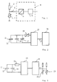
- Fig. 1 shows a circuit for performing the method.
- resistors 1 and 2 form a voltage divider whose output voltage on line 3 is passed on to a processor 5 for reading in via an analog / digital converter 4.
- Advantages compared to a direct adjustment of the electronic circuit can also be achieved if a complex iterative adjustment process is omitted by a formal consideration of the set parameters, or if an expensive adjustment using a trimming capacitor can be replaced by the resistance adjustment.
- the comparison can only take place via an iterative process; This means that the measuring capacitance must be filled alternately with media of different dielectric constants and in each case an adjustment of the capacitor 17 in the presence of a low dielectric constant and the resistance trimmer 18 in the presence of a medium with a high dielectric constant must be set until such time as no significant improvement the setting can be achieved more.
- the method according to the invention is used.
- the trimming capacitor 17 (FIG. 2) can be omitted and the trimming resistor 18 (FIG. 2) can be converted into a fixed resistor 21.
- the adjustment is now carried out in such a way that one frequency measurement is carried out with a medium with a low dielectric constant (e.g. air) and a second measurement with a medium with a particularly high dielectric constant.
- the result of the frequency measurement is entered into the processor by trimming two resistors 22 and 23, so that it can then compensate for the series spread in future operation by taking into account a corresponding formula.
- the method on which the invention is based can also be used very advantageously in order to adapt each copy of a series to the specific application. For example, a selection of output characteristics can be made by coding with different analog values.
- an individually programmable module can be saved for programming a serial number, batch number, a product type identification or for implementing software protection by setting the parameters again by means of resistance trimming and making them available to the processor via A / D converters.
- hybrid circuits can be integrated particularly advantageously into the housing of sensors, which are compensated for by the type variation and e.g. Adaptation of the output characteristic of the sensor by the processor to the specific application to provide an immediately reusable signal.
Landscapes
- Engineering & Computer Science (AREA)
- Physics & Mathematics (AREA)
- General Physics & Mathematics (AREA)
- Theoretical Computer Science (AREA)
- General Engineering & Computer Science (AREA)
- Quality & Reliability (AREA)
- Human Computer Interaction (AREA)
- Semiconductor Integrated Circuits (AREA)
- Analogue/Digital Conversion (AREA)
- Measurement Of Resistance Or Impedance (AREA)
Description
Die Erfindung bezieht sich auf ein Verfahren zur Einstellung von elektronischen Schaltungen, welche einen oder mehrere Widerstände und einen oder mehrere Prozessoren enthalten.The invention relates to a method for setting electronic circuits which contain one or more resistors and one or more processors.
Bei zahlreichen elektronischen Schaltungen ist für jedes produzierte Exemplar ein separater Abgleich zur Korrektur von Bauteiltoleranzen oder auch zur Abstimmung auf spezifische Anforderungen notwendig. Zu diesem Zweck wird häufig ein Abgleich von einem oder mehreren elektronischen Bauteilen, wie z.B. Kondensatoren, vorgenommen.With numerous electronic circuits, a separate adjustment is necessary for the correction of component tolerances or for adjustment to specific requirements for each copy produced. For this purpose, a comparison of one or more electronic components, e.g. Capacitors.
Bei elektronischen Schaltungen, die einen Prozessor enthalten, kann der Aufwand durch Verwendung von elektronisch programmierbaren Bausteinen, wie z.B. PROM oder EPROM, reduziert werden (siehe z.B. GB-A-2 197 957), indem die Anpassung jedes Exemplars durch Einprogrammieren von entsprechenden Parametern durchgeführt wird (Band-Ende-Programmierung). Dies erfordert allerdings das Vorhandensein solcher einzeln programmierbarer Bausteine, deren Kosten deutlich über denen eines z.B. maskenprogrammierten Bausteins liegen.For electronic circuits that contain a processor, the effort can be reduced by using electronically programmable modules, such as PROM or EPROM, can be reduced (see e.g. GB-A-2 197 957) by adapting each item by programming the appropriate parameters (end-of-tape programming). However, this requires the existence of such individually programmable modules, the costs of which are significantly higher than those of e.g. mask-programmed block.
Aus GB-A-2 054 301 ist eine Anordnung bekannt, in der ein einstellbarer Widerstandswert über einen ADU laufend in einen Prozessor eingelesen wird, um Einstellungen vorzunehmen.From GB-A-2 054 301 an arrangement is known in which an adjustable resistance value is continuously read into a processor via an ADC in order to make settings.
Der Erfindung liegt die Aufgabe zugrunde, eine kostengünstige und flexible Programmierung auch bei ausschließlicher Verwendung von festen Programmspeichern, wie maskenprogrammierbaren ROMs, zu ermöglichen.The invention is based on the object of enabling inexpensive and flexible programming even when only using fixed program memories, such as mask-programmable ROMs.
Diese Aufgabe wird durch die Merkmale des Anspruchs 1 gelöst.This object is solved by the features of
Aufgrund des besonders einfachen Widerstandsabgleichs ist eine "Programmierunq" von Parametern möglich, auf die der Prozessor ähnlich wie bei der PROM-Lösung zugreifen kann.Due to the particularly simple resistance adjustment, a "programming" of parameters is possible, which the processor can access similar to the PROM solution.
Ausführungsbeispiele der Erfindung werden nachfolgend anhand der Zeichnungen beschrieben.Embodiments of the invention are described below with reference to the drawings.
Fig. 1 zeigt eine Schaltung zur Durchführung des Verfahrens.Fig. 1 shows a circuit for performing the method.
Fig. 2 und 3 zeigen Schaltungen zur Messung der Dielektrizitätszahl eines unbekannten Mediums.2 and 3 show circuits for measuring the dielectric constant of an unknown medium.
Wie Fig. 1 zeigt, wird von Widerständen 1 und 2 ein Spannungsteiler gebildet, dessen Ausgangsspannung auf Leitung 3 über einen Analog/Digital-Umsetzer 4 einem Prozessor 5 zum Einlesen weitergegeben wird.As shown in FIG. 1,
Besondere Vorteile bezüglich der kostengünstigen Realisierung sind erreichbar, wenn der Analog/Digital-Umsetzer 4 mit dem Prozessor 5 zusammen in einem Mikro-Controller 6 integriert ist.Particular advantages with regard to the cost-effective implementation can be achieved if the analog / digital converter 4 and the
Vorteile gegenüber einem direkten Abgleich der elektronischen Schaltung lassen sich auch erzielen, wenn durch eine formelmäßige Berücksichtigung der eingestellten Farameter ein aufwendiger iterativer Einstellvorgang entfällt, oder wenn hierdurch eine aufwendige Einstellung mittels Trimmkondensator durch den Widerstandsabgleich ersetzt werden kann.Advantages compared to a direct adjustment of the electronic circuit can also be achieved if a complex iterative adjustment process is omitted by a formal consideration of the set parameters, or if an expensive adjustment using a trimming capacitor can be replaced by the resistance adjustment.
Beispielsweise ist in Figur 2 eine Schaltung zur Messung der Dielektrizitätszahl eines unbekannten Mediums dargestellt, wobei das Medium das Dielektrikum 11 eines Kondensators 12 bildet, der das frequenzbestimmende Glied in einem RC-Schwingkreis 13 ist. Bedingt durch Fertigungsstreuungen schwankt sowohl die von der Dielektrizitätszahl abhängige Kapazität 12 als auch die von der Dielektrizitätszahl unabhängige parasitäre Kapazität 14. Um nun einen Abgleich der Ausgangsfrequenz auf Leitung 15, die einer Weiterverarbeitungsschaltung 16 zugeführt wird, über den gesamten Meßbereich vornehmen zu können, ist ein Abgleich mit Hilfe von zwei einstellbaren Komponenten, nämlich einem Parallelkondensator 17 und einem Trimmwiderstand 18, erforderlich. Der Abgleich kann nur über einen iterativen Prozess erfolgen; das bedeutet, daß die Meßkapazität wechselweise mit Medien verschiedener Dielektrizitätszahl befüllt werden muß und jeweils ein Abgleich des Kondensators 17 bei Vorhandensein einer niedrigen Dielektrizitätszahl und der Widerstandstrimmer 18 bei Vorhandensein eines Mediums mit hoher Dielektrizitätszahl eingestellt werden muß, und zwar so lange, bis keine deutliche Verbesserung der Einstellung mehr erzielt werden kann.For example, FIG. 2 shows a circuit for measuring the dielectric constant of an unknown medium, the medium forming the dielectric 11 of a
In der Ausführungsform gemäß Figur 3 kommt das Verfahren gemäß der Erfindung zur Anwendung. Hierbei kann der Trimmkondensator 17 (Fig. 2) entfallen und der Trimmwiderstand 18 (Fig. 2) in einen Festwiderstand 21 umgewandelt werden. Der Abgleich erfolgt nun in der Weise, daß einmal eine Frequenzmessung mit einem Medium niedriger Dielektrizitätszahl (z.B. Luft) und eine zweite Messung mit einem Medium besonders hoher Dielektrizitätszahl durchgeführt wird. Das Ergebnis der Frequenzmessung wird durch Trimmung von zwei Widerständen 22 und 23 dem Prozessor eingegeben, so daß er dann bei zukünftigem Betrieb durch eine entsprechende formelmäßige Berücksichtigung eine Kompensation der Serienstreuung vornehmen kann.In the embodiment according to FIG. 3, the method according to the invention is used. The trimming capacitor 17 (FIG. 2) can be omitted and the trimming resistor 18 (FIG. 2) can be converted into a
Für die Großserienfertigung sind besondere Vorteile erzielbar durch den Einsatz eines Widerstands-Laser-Trimmverfahrens, das bei der konventionellen Technik aus zwei Gründen nicht eingesetzt werden könnte. Zum einen gibt es keine sinnvolle Möglichkeit, einen Kondensator durch Lasertrimmung abzugleichen, und zum anderen ist verfahrensbedingt bei der Lasertrimmung ein iterativer Abgleich nicht möglich (Abgleich durch teilweises Wegbrennen der Widerstandsbahnen).For large-scale production, special advantages can be achieved by using a resistance laser trimming process, which could not be used in conventional technology for two reasons. On the one hand, there is no sensible way to adjust a capacitor by laser trimming, and on the other hand, due to the process, laser trimming is an iterative process Adjustment not possible (adjustment due to partial burning away of the resistance tracks).
Ebenfalls sehr vorteilhaft kann das der Erfindung zugrunde liegende Verfahren verwendet werden, um für jedes Exemplar einer Serie eine Anpassung an den spezifischen Anwendungsfall vorzunehmen. So kann z.B. durch Kodieren mit verschiedenen Analogwerten eine Auswahl von Ausgangskennlinien vorgenommen werden.The method on which the invention is based can also be used very advantageously in order to adapt each copy of a series to the specific application. For example, a selection of output characteristics can be made by coding with different analog values.
Weiterhin läßt sich ein einzeln programmierbarer Baustein einsparen für eine Programmierung einer Seriennummer, Chargennummer, einer Produkttypenkennzeichnung oder für die Realisierung eines Softwareschutzes, indem die Parameter wiederum durch Widerstandstrimmung eingestellt und über A/D-Umsetzer dem Prozessor zur Verfügung gestellt werden.Furthermore, an individually programmable module can be saved for programming a serial number, batch number, a product type identification or for implementing software protection by setting the parameters again by means of resistance trimming and making them available to the processor via A / D converters.
Besonders vorteilhaft ist der Einsatz dieser gesamten Verfahren in der Hybridtechnik, wo insbesondere die Lasertrimmung zum Tragen kommt. Solche Hybridschaltungen können besonders vorteilhaft in die Gehäuse von Sensoren integriert werden, die durch Kompensation der Typenstreuung und z.B. Anpassung der Ausgangskennlinie des Sensors durch den Prozessor an die spezifische Anwendung ein unmittelbar weiterverwendbares Signal zur Verfügung stellen.It is particularly advantageous to use these entire processes in hybrid technology, where laser trimming is particularly important. Such hybrid circuits can be integrated particularly advantageously into the housing of sensors, which are compensated for by the type variation and e.g. Adaptation of the output characteristic of the sensor by the processor to the specific application to provide an immediately reusable signal.
Claims (7)
- A procedure for adjusting electronic measuring circuits which contain at least one adjustable resistance and at least one processor, characterised by the procedural steps that the resistance is adjusted to a predeterminable value of the quantity to measured in subsequent operation, that by means of an analogue-digital converter the adjusted resistance value corresponding to a parameter of measurement in subsequent operation of the circuit is permanently available to the processor for reading in, and that the adjusted resistance value is read in and taken into consideration during measurements of unknown values of the quantity to be measured in subsequent operation of the circuit for the correction of the output signal of the measuring circuit.
- A procedure according to claim 1, characterised in that at least one parameter is used for the compensation of production tolerances.
- A procedure according to claim 1, characterised in that at least one parameter is used for adapting to different applications.
- A procedure according to claim 1, characterised in that at least one parameter is used for the identification of the circuit, e.g. of the serial number, the batch number, the product type or the software protection.
- A procedure according to any one of claims 1-4, characterised in that the adjustment of at least one resistance is effected by laser trimming.
- A procedure according to any one of claims 1-5, characterised in that at least one parameter is processed according to a formula.
- A procedure according to any one of claims 1-6, characterised in that the electronic circuit is accommodated in a common housing with a measured value sensor.
Priority Applications (4)
| Application Number | Priority Date | Filing Date | Title |
|---|---|---|---|
| EP89112816A EP0407639B1 (en) | 1989-07-13 | 1989-07-13 | Method of preadjusting electronic circuits |
| DE58909651T DE58909651D1 (en) | 1989-07-13 | 1989-07-13 | Method of setting electronic circuits |
| JP2179722A JPH03116861A (en) | 1989-07-13 | 1990-07-09 | Method of adjusting electronic circuit |
| US07/551,175 US5103075A (en) | 1989-07-13 | 1990-07-11 | Process for the adjustment of electronic circuits |
Applications Claiming Priority (1)
| Application Number | Priority Date | Filing Date | Title |
|---|---|---|---|
| EP89112816A EP0407639B1 (en) | 1989-07-13 | 1989-07-13 | Method of preadjusting electronic circuits |
Publications (2)
| Publication Number | Publication Date |
|---|---|
| EP0407639A1 EP0407639A1 (en) | 1991-01-16 |
| EP0407639B1 true EP0407639B1 (en) | 1996-04-10 |
Family
ID=8201615
Family Applications (1)
| Application Number | Title | Priority Date | Filing Date |
|---|---|---|---|
| EP89112816A Expired - Lifetime EP0407639B1 (en) | 1989-07-13 | 1989-07-13 | Method of preadjusting electronic circuits |
Country Status (4)
| Country | Link |
|---|---|
| US (1) | US5103075A (en) |
| EP (1) | EP0407639B1 (en) |
| JP (1) | JPH03116861A (en) |
| DE (1) | DE58909651D1 (en) |
Families Citing this family (1)
| Publication number | Priority date | Publication date | Assignee | Title |
|---|---|---|---|---|
| US6875950B2 (en) * | 2002-03-22 | 2005-04-05 | Gsi Lumonics Corporation | Automated laser trimming of resistors |
Family Cites Families (7)
| Publication number | Priority date | Publication date | Assignee | Title |
|---|---|---|---|---|
| US4284872A (en) * | 1978-01-13 | 1981-08-18 | Burr-Brown Research Corporation | Method for thermal testing and compensation of integrated circuits |
| GB2054301B (en) * | 1979-06-19 | 1982-09-02 | Gec Elliott Automation Ltd | Generating digital signals adc with nonvolatile input |
| US4381441A (en) * | 1980-10-30 | 1983-04-26 | Western Electric Company, Inc. | Methods of and apparatus for trimming film resistors |
| JPS58115547A (en) * | 1981-12-29 | 1983-07-09 | Fujitsu Ltd | Operation mode setting system for microprocessor |
| FR2587515B1 (en) * | 1985-09-17 | 1989-09-08 | Esswein Sa | DEVICE FOR ENTERING DATA IN A MICRO-PROCESSOR |
| DE3610170A1 (en) * | 1986-03-26 | 1987-10-01 | Bosch Gmbh Robert | Method for calibrating a measurement circuit |
| GB2197957B (en) * | 1986-11-22 | 1990-10-17 | Motorola Ltd | Sensor systems |
-
1989
- 1989-07-13 DE DE58909651T patent/DE58909651D1/en not_active Expired - Fee Related
- 1989-07-13 EP EP89112816A patent/EP0407639B1/en not_active Expired - Lifetime
-
1990
- 1990-07-09 JP JP2179722A patent/JPH03116861A/en active Pending
- 1990-07-11 US US07/551,175 patent/US5103075A/en not_active Expired - Lifetime
Also Published As
| Publication number | Publication date |
|---|---|
| JPH03116861A (en) | 1991-05-17 |
| DE58909651D1 (en) | 1996-05-15 |
| EP0407639A1 (en) | 1991-01-16 |
| US5103075A (en) | 1992-04-07 |
Similar Documents
| Publication | Publication Date | Title |
|---|---|---|
| DE10156027B4 (en) | Adjustable filter circuit | |
| DE69216554T2 (en) | Method and device for the automatic tuning calibration of electronically tuned filters | |
| DE69425160T2 (en) | DEVICE FOR MEASURING MATERIAL PROPERTY | |
| WO2008064500A2 (en) | System for measuring a physical variable | |
| DE4313390A1 (en) | Capacitive detector for vehicle occupants - forms capacitor from ground and seat electrodes and senses failure of electrodes, processor and input signal processor using capacitance of input switching part. | |
| DE3704624A1 (en) | METHOD FOR MEASURING IMPEDANCES, SPECIFICALLY SMALL CAPACITIES | |
| DE3822407A1 (en) | OSCILLATOR CIRCUIT WITH DIGITAL TEMPERATURE COMPENSATION | |
| EP0377782B1 (en) | Method for the determination of the alcohol content and/or the calorific value of fuels | |
| DE4326373C2 (en) | Device for detecting the alcohol content of a liquid | |
| DE69006740T2 (en) | CAPACITIVE PRESSURE SENSOR SYSTEM. | |
| DE1498819C3 (en) | Device for determining a characteristic property of a material | |
| EP0407639B1 (en) | Method of preadjusting electronic circuits | |
| EP0464391B1 (en) | Measuring device and method for putting it into operation | |
| DE10121517A1 (en) | Method and device for setting an active filter | |
| DE4109914A1 (en) | TIMELY STABLE HF FILTER | |
| DE3887916T2 (en) | Circuit for automatically controlling the gain-bandwidth product of operational amplifiers. | |
| DE2702815C3 (en) | Temperature measuring device | |
| DE2002168C3 (en) | Dielectric humidity measuring device | |
| WO2013164152A1 (en) | Circuit arrangement for measuring a sensor element capacitance | |
| DE3519390C2 (en) | ||
| EP0532781B1 (en) | Integrated circuit comprising an analog circuit | |
| EP0561054A1 (en) | Apparatus and procedure for measuring the time-constant of an electrical displacement transducer | |
| DE2933840C2 (en) | Circuit arrangement for checking and controlling the coefficients of an analog adaptive equalizer | |
| EP0042881B1 (en) | Method and apparatus for testing a metallic test piece | |
| EP0057368A2 (en) | Digital length or angle position measuring device |
Legal Events
| Date | Code | Title | Description |
|---|---|---|---|
| PUAI | Public reference made under article 153(3) epc to a published international application that has entered the european phase |
Free format text: ORIGINAL CODE: 0009012 |
|
| AK | Designated contracting states |
Kind code of ref document: A1 Designated state(s): DE FR GB IT SE |
|
| 17P | Request for examination filed |
Effective date: 19901224 |
|
| 17Q | First examination report despatched |
Effective date: 19930812 |
|
| GRAH | Despatch of communication of intention to grant a patent |
Free format text: ORIGINAL CODE: EPIDOS IGRA |
|
| GRAA | (expected) grant |
Free format text: ORIGINAL CODE: 0009210 |
|
| AK | Designated contracting states |
Kind code of ref document: B1 Designated state(s): DE FR GB IT SE |
|
| PG25 | Lapsed in a contracting state [announced via postgrant information from national office to epo] |
Ref country code: IT Free format text: LAPSE BECAUSE OF FAILURE TO SUBMIT A TRANSLATION OF THE DESCRIPTION OR TO PAY THE FEE WITHIN THE PRE;WARNING: LAPSES OF ITALIAN PATENTS WITH EFFECTIVE DATE BEFORE 2007 MAY HAVE OCCURRED AT ANY TIME BEFORE 2007. THE CORRECT EFFECTIVE DATE MAY BE DIFFERENT FROM THE ONE RECORDED.SCRIBED TIME-LIMIT Effective date: 19960410 |
|
| REF | Corresponds to: |
Ref document number: 58909651 Country of ref document: DE Date of ref document: 19960515 |
|
| GBT | Gb: translation of ep patent filed (gb section 77(6)(a)/1977) |
Effective date: 19960507 |
|
| PGFP | Annual fee paid to national office [announced via postgrant information from national office to epo] |
Ref country code: GB Payment date: 19960625 Year of fee payment: 8 |
|
| ET | Fr: translation filed | ||
| PGFP | Annual fee paid to national office [announced via postgrant information from national office to epo] |
Ref country code: FR Payment date: 19960705 Year of fee payment: 8 |
|
| PG25 | Lapsed in a contracting state [announced via postgrant information from national office to epo] |
Ref country code: SE Effective date: 19960710 |
|
| PLBE | No opposition filed within time limit |
Free format text: ORIGINAL CODE: 0009261 |
|
| STAA | Information on the status of an ep patent application or granted ep patent |
Free format text: STATUS: NO OPPOSITION FILED WITHIN TIME LIMIT |
|
| 26N | No opposition filed | ||
| PG25 | Lapsed in a contracting state [announced via postgrant information from national office to epo] |
Ref country code: GB Free format text: LAPSE BECAUSE OF NON-PAYMENT OF DUE FEES Effective date: 19970713 |
|
| GBPC | Gb: european patent ceased through non-payment of renewal fee |
Effective date: 19970713 |
|
| PG25 | Lapsed in a contracting state [announced via postgrant information from national office to epo] |
Ref country code: FR Free format text: LAPSE BECAUSE OF NON-PAYMENT OF DUE FEES Effective date: 19980331 |
|
| REG | Reference to a national code |
Ref country code: FR Ref legal event code: ST |
|
| PGFP | Annual fee paid to national office [announced via postgrant information from national office to epo] |
Ref country code: DE Payment date: 20040720 Year of fee payment: 16 |
|
| PG25 | Lapsed in a contracting state [announced via postgrant information from national office to epo] |
Ref country code: DE Free format text: LAPSE BECAUSE OF NON-PAYMENT OF DUE FEES Effective date: 20060201 |