EP0405857A2 - Waveguide type photoswitch with a short coupling region - Google Patents
Waveguide type photoswitch with a short coupling region Download PDFInfo
- Publication number
- EP0405857A2 EP0405857A2 EP90306852A EP90306852A EP0405857A2 EP 0405857 A2 EP0405857 A2 EP 0405857A2 EP 90306852 A EP90306852 A EP 90306852A EP 90306852 A EP90306852 A EP 90306852A EP 0405857 A2 EP0405857 A2 EP 0405857A2
- Authority
- EP
- European Patent Office
- Prior art keywords
- coupling region
- electrodes
- waveguide paths
- waveguide
- photoswitch
- Prior art date
- Legal status (The legal status is an assumption and is not a legal conclusion. Google has not performed a legal analysis and makes no representation as to the accuracy of the status listed.)
- Granted
Links
Images
Classifications
-
- G—PHYSICS
- G02—OPTICS
- G02F—OPTICAL DEVICES OR ARRANGEMENTS FOR THE CONTROL OF LIGHT BY MODIFICATION OF THE OPTICAL PROPERTIES OF THE MEDIA OF THE ELEMENTS INVOLVED THEREIN; NON-LINEAR OPTICS; FREQUENCY-CHANGING OF LIGHT; OPTICAL LOGIC ELEMENTS; OPTICAL ANALOGUE/DIGITAL CONVERTERS
- G02F1/00—Devices or arrangements for the control of the intensity, colour, phase, polarisation or direction of light arriving from an independent light source, e.g. switching, gating or modulating; Non-linear optics
- G02F1/29—Devices or arrangements for the control of the intensity, colour, phase, polarisation or direction of light arriving from an independent light source, e.g. switching, gating or modulating; Non-linear optics for the control of the position or the direction of light beams, i.e. deflection
- G02F1/31—Digital deflection, i.e. optical switching
- G02F1/313—Digital deflection, i.e. optical switching in an optical waveguide structure
- G02F1/3132—Digital deflection, i.e. optical switching in an optical waveguide structure of directional coupler type
Definitions
- the present invention relates to a photoswitch of the type electrically switching over the direction in which an optical signal is propagated through a waveguide path.
- a waveguide type photoswitch has been proposed in various forms in, for example, JOURNAL OF LIGHTWAVE TECHNOLOGY, LT-4 [9], pp. 1324-1327, 1986-1989 (hereinafter referred to as document 1), Nishihara et al "Optical Integrated Circuit", Ist Edition, Ohm-Sha, pp. 304-307, Feburary 25, 1985, (hereinafter referred to as document 2), and Japanese Patent Application No. 295872/1987 (hereinafter referred to as document 3).
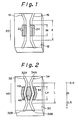
- FIG. 1 shows a specific structure of a conventional waveguide type photoswitch adopting a directional coupler system, as disclosed in the document 1.
- the photoswitch has a substrate 12 exhibiting an electrooptical effect, a pair of waveguide paths 14 and 16 formed on the substrate 12 in close proximity to each other, and electrodes 22 and 24 provided in a coupling region 20 which couples waveguide paths 14 and 16.
- the refractive indexes n0 of the waveguide paths 14 and 16 are controlled by an operating voltage vo which is applied between the electrodes 22 and 24.
- the coupling region 20 has a length l
- the electrodes 22 and 24 each has a length l e which is smaller than the length l .
- the length l of the coupling region 20 is selected such that while the operating voltage vo is not applied, light entering the waveguide path 14 or 16 is outputted from the waveguide path 16 or 14, i. e. in a cross condition.
- the refractive index difference ⁇ n0 mentioned above is proportional to the operating voltage vo, while the electrode capacitance decreases with the decrease of l e of the individual electrodes 22 and 24. It follows that the smaller the left member, 2 ⁇ n0 l e/ ⁇ , of the Eq. (1), i. e. , the smaller the value of ⁇ n0 l e, the lower the operating voltage vo is. This is successful in reducing the electrode capacitance and thereby enhancing high-speed operation.
- the waveguide paths 14 and 16 will be brought into a bar condition if the refractive index difference ⁇ n0 has a particular value expressed as:
- the result of the Eq. (2) sequentially approaches ⁇ and may, therefore, be made smaller than the result of the Eq. (1). More specifically, the product ⁇ n0 l e is smaller in the Eq. (2) than in the Eq. (1).
- a problem with the prior art photoswitch having the above structure is as follows. Assuming that the refractive index difference ⁇ n0 is constant, a decrease in the length l e of the individual electrodes 22 and 24 results in an increase in the length l of the coupling region 20. Specifically, the refractive index difference ⁇ n0 and the length l of the coupling region 20 are related as:
- the value of the left member increases as the value of l e/ l included in the right member is reduced toward zero. More specifically, assuming that the refractive index difference ⁇ n0 is constant, the length l of the coupling region 20 increases with the decrease in the length l e of the electrodes 22 and 24. This is acceptable so long as the waveguide type photoswitch is used alone. However, when such a photoswitch is integrated in a plurality of stages on a semiconductor substrate, for example, the coupling region 20 having a greater length would undesirably add to the required area of the substrate.
- the document 2 teaches a waveguide type photoswitch elaborated to eliminate the above-discussed problem particular to the photoswitch of the document 1.
- the switch of the document 3 has two waveguide paths arranged side by side on a substrate which exhibits an electrooptical effect. Electrodes are disposed in the coupling region of the two waveguide paths. The distance between the waveguide paths sequentially increases from opposite ends toward the center of the coupling region. In such a switch configuration, the coupling coefficient of the two waveguide paths decreases with the increase in the distance between the waveguide paths. Hence, reducing the coupling coefficient in the position where the two waveguide paths are greatly spaced from each other allows the length of the coupling region to be reduced and the operating voltage to be lowered. Such an approach, however, is not fully satisfactory because it cannot lower the operating voltage beyond a certain level or increase the operating speed to a sufficient degree.
- a waveguide type photoswitch of the present invention comprises a substrate, a plurality of waveguide paths formed on the substrate side by side, and a plurality of electrodes arranged in a coupling region of the waveguide paths.
- the waveguide paths are configured such that the distance between the paths is greater at the center of the coupling region than at opposite ends of the coupling region.
- the electrodes extend along the waveguide paths and each has a length smaller than that of the coupling region.
- a waveguide type photoswitch embodying the present invention is shown. Also shown in the figure is a parameter ⁇ representative of a distance as measured from the center of a coupling region 40 which will be described.
- the photoswitch has a substrate 30 implemented with a lithium niobate (LiNbO3) monocrystal which has an electrooptical effect.
- Two waveguide paths 32 and 34 are formed on the substrate 30 in close proximity to each other.
- the waveguide path 32 has an input port 32A and output port 32B, while the waveguide path 34 has an input port 34A and an output port 34B.
- the distance between the waveguide paths 32 and 34 is reduced at opposite ends of the coupling region 40 in order to couple optically between the waveguide paths 32 and 34, and it is sequentially increased toward the center of the coupling region 40.
- Electrodes 42 and 44 are positioned in the coupling region 40 to extend along the outer side end of the waveguide paths 32 and 34, respectively.
- An electrode 46 is also located in the coupling region 40 between the inner side end of the waveguide paths 32 and 34.
- the coupling region 40 has a length L while the electrodes 42, 44 and 46 each has a length Le which is smaller than the length L.
- the length L of the coupling region 40 is selected such that while no voltage is applied between the electrodes 42, 44 an 46, light entered the input port 32A or 34A is emitted via the output port 34B or 32B in a cross condition.
- the operation of the photoswitch constructed as shown in FIG. 2 may be represented by an equation, as follows: where ⁇ is the complex amplitude ratio, ⁇ is the parameter representative of the distance as measured from the center of the coupling region 40, ⁇ is the difference in propagation constant between the waveguide paths 32 and 34, and ⁇ ( ⁇ ) is the coupling coefficient.
- ⁇ is equal to 2 ⁇ n/ ⁇ , where ⁇ n and ⁇ are the difference in refractive index electrically induced between the waveguide paths 32 and 34 and the waveform of light in vacuum, respectively.
- the value of ⁇ ( ⁇ ) L included in the Eq. (4) may be represented by a ratio R of the minimum coupling coefficient ⁇ min to the maximum coupling coefficient ⁇ max , with no regard to the formation of the function. It is to be noted that the minimum and maximum coupling coefficients ⁇ min and ⁇ max are respectively the values measured at the center and opposite ends of the coupling region 40.
- the length L of the coupling region 40 is selected to be an odd multiple of the coupling length L0.
- L is selected to be equal to L0.
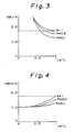
- FIG. 3 shows a product ⁇ L characteristic and indicates the values of ⁇ L/ ⁇ and Le/L on its ordinate and abscissa, respectively.
- sequentially reducing the length Le of the individual electrodes 42, 44 and 46 while maintaining the voltage (i. e. ⁇ ) constant causes the length L of the coupling region 40 to increase.
- FIG. 4 shows a product ⁇ Le characteristics and indicates the values of ⁇ Le/ ⁇ and Le/L on its ordinate and abscissa, respectively.
- the value of ⁇ Le/ ⁇ further decreases when the length Le of the individual electrodes 42, 44 and 46 is reduced.
- the above system is caused into a cross condition when the phase difference is ⁇ and ⁇ into a bar state when it is 2 ⁇ .
- the coupling constant ⁇ is zero at and in the vicinity of the center of the coupling region 40 and can be provided with a sufficiently large value at opposite ends of the coupling region 40, compared to the value ⁇ .
- the produce ⁇ L sequentially decreases. Therefore, assuming that the voltage (i. e. ⁇ ) is constant, the length L of the coupling region 40 decreases as the distance between the waveguide paths 32 and 34 increases ( ⁇ ⁇ decreases toward zero).
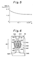
- FIG. 6 shows an alternative embodiment of the present invention.
- the same components are designated by like reference numerals, and redundant description will be avoided for simplicity.
- the embodiment of FIG. 6 differs from that of FIG. 2 concerning the configuration of the three electrodes 42, 44 and 46.
- electrodes 42B, 44B and 46B shown in FIG. 6 are substantially identical in configuration with the electrodes 42, 44 and 46 of FIG. 2, each of them is made up of three segments, as illustrated. Specifically, electrodes 42A, 44A and 46A and electrodes 42C, 44C and 46C are positioned on the substrate 30 at opposite sides of the electrodes 42B, 44B and 46B, respectiely.
- a bar condition is set up when a positive drive voltage +V or a negative drive voltage -V is applied between the electrodes 42B and 44B.
- the switch of FIG. 6 is capable of setting up a cross condition more accurately than the switch of FIG. 2 by having the bias voltage finely adjusted, thereby further improving the ratio of light propagated crosswise in a bar condition.
- the present invention provides a waveguide type photoswitch which is operable with a lower drive voltage and, therefore, with a relatively short coupling region.
- This unprecedented advantage is derived from a unique configuration wherein the distance between nearby waveguides is gradually increased from opposite ends toward the center of the coupling region.
- the photoswitch is provided with electrodes each being shorter than the coupling region, the drive voltage is noticeably reduced and high-speed operation is enhanced.
- the electrodes 42 and 44 shown in FIG. 2 may be configured to overlap the waveguide paths 32 and 34, respectively.
- the intermediate electrode 46 may be configured to overlap the waveguide paths 32 and 34.
- the electrode 46 intervening between the electrodes 42 and 44 as shown in FIG. 2 may be omitted in which case the electrodes 42 and 44 will be extended to overlap the waveguides 32 and 34, respectively.
- a bar condition will be set up when a positive or a negative drive voltage is applied to the electrode 44 or 42 with the electrode 42 or 44 being connected to ground, while a cross condition will be set up when such a drive voltage is not applied.
- the waveguide paths 32 and 34 may each be provided with an arcuate or similar shape other than the angled shape shown and described. Then, the electrodes may also be provided with a particular configuration complementary to the waveguide paths.
- the substrate 30 may be implemented as a monocrystalline substrate of LiTaO3 or similar compound, a substrate of InGaAsP, GaAlAs or similar compound semiconductor, etc.
Abstract
Description
- The present invention relates to a photoswitch of the type electrically switching over the direction in which an optical signal is propagated through a waveguide path.
- A waveguide type photoswitch has been proposed in various forms in, for example, JOURNAL OF LIGHTWAVE TECHNOLOGY, LT-4 [9], pp. 1324-1327, 1986-1989 (hereinafter referred to as document 1), Nishihara et al "Optical Integrated Circuit", Ist Edition, Ohm-Sha, pp. 304-307, Feburary 25, 1985, (hereinafter referred to as document 2), and Japanese Patent Application No. 295872/1987 (hereinafter referred to as document 3).
- FIG. 1 shows a specific structure of a conventional waveguide type photoswitch adopting a directional coupler system, as disclosed in the
document 1. The photoswitch has asubstrate 12 exhibiting an electrooptical effect, a pair ofwaveguide paths substrate 12 in close proximity to each other, andelectrodes coupling region 20 whichcouples waveguide paths coupling region 20, the refractive indexes n₀ of thewaveguide paths electrodes coupling region 20 has a length l, theelectrodes coupling region 20 is selected such that while the operating voltage vo is not applied, light entering thewaveguide path waveguide path - The operating voltage vo applied between the
electrodes waveguide paths waveguide path individual electrodes waveguide path same waveguide path waveguide paths 
- The refractive index difference Δn₀ mentioned above is proportional to the operating voltage vo, while the electrode capacitance decreases with the decrease of le of the
individual electrodes - When the
electrodes waveguide paths 
- As the value of le/l included in the right member of the Eq. (2) is sequentially decreased toward zero, the result of the Eq. (2) sequentially approaches π and may, therefore, be made smaller than the result of the Eq. (1). More specifically, the product Δn₀le is smaller in the Eq. (2) than in the Eq. (1).
- It has been customary to provide electrodes each having a small length le in the
coupling region 20 so as to lower the operating voltage vo and to thereby enhance high-speed operation. - A problem with the prior art photoswitch having the above structure is as follows. Assuming that the refractive index difference Δn₀ is constant, a decrease in the length le of the
individual electrodes coupling region 20. Specifically, the refractive index difference Δn₀ and the length l of thecoupling region 20 are related as:
- In the above Eq. (3), the value of the left member increases as the value of le/l included in the right member is reduced toward zero. More specifically, assuming that the refractive index difference Δn₀ is constant, the length l of the
coupling region 20 increases with the decrease in the length le of theelectrodes coupling region 20 having a greater length would undesirably add to the required area of the substrate. - The document 2 teaches a waveguide type photoswitch elaborated to eliminate the above-discussed problem particular to the photoswitch of the
document 1. The switch of the document 3 has two waveguide paths arranged side by side on a substrate which exhibits an electrooptical effect. Electrodes are disposed in the coupling region of the two waveguide paths. The distance between the waveguide paths sequentially increases from opposite ends toward the center of the coupling region. In such a switch configuration, the coupling coefficient of the two waveguide paths decreases with the increase in the distance between the waveguide paths. Hence, reducing the coupling coefficient in the position where the two waveguide paths are greatly spaced from each other allows the length of the coupling region to be reduced and the operating voltage to be lowered. Such an approach, however, is not fully satisfactory because it cannot lower the operating voltage beyond a certain level or increase the operating speed to a sufficient degree. - It is therefore an object of the present invention to provide a waveguide type photoswitch which reduces the length of the coupling region of waveguide paths.
- It is another object of the present invention to provide a waveguide type photoswitch which is operable with a far lower operating voltage than the prior art.
- It is yet another object of the present invention to provide a waveguide type photoswitch which is operable at a sufficiently high speed.
- A waveguide type photoswitch of the present invention comprises a substrate, a plurality of waveguide paths formed on the substrate side by side, and a plurality of electrodes arranged in a coupling region of the waveguide paths. The waveguide paths are configured such that the distance between the paths is greater at the center of the coupling region than at opposite ends of the coupling region. The electrodes extend along the waveguide paths and each has a length smaller than that of the coupling region.
- The objects and features of the present invention will become more apparent from the consideration of the following detailed description taken in conjunction with the accompanying drawings in which:
- FIG. 1 is a perspective view of a prior art waveguide type photoswitch;
- FIG. 2 is a perspective view of a waveguide type photoswitch embodying the present invention;
- FIG. 3 is a graph representative of a product ΔβL characteristic particular to the switch shown in FIG. 2;
- FIG. 4 is a graph showing a product ΔβLe characteristic also particular to the switch of FIG. 2;
- FIG. 5 is a graph showing a product ΔβLe characteristic of the illustrative embodiment which holds in a condition of L = Le; and
- FIG. 6 is a perspective view showing an alternative embodiment of the present invention.
- Referring to FIG. 2, a waveguide type photoswitch embodying the present invention is shown. Also shown in the figure is a parameter τ representative of a distance as measured from the center of a
coupling region 40 which will be described. - In FIG. 2, the photoswitch has a
substrate 30 implemented with a lithium niobate (LiNbO₃) monocrystal which has an electrooptical effect. Twowaveguide paths substrate 30 in close proximity to each other. Thewaveguide path 32 has aninput port 32A andoutput port 32B, while thewaveguide path 34 has aninput port 34A and anoutput port 34B. In thecoupling region 40 of thewaveguides waveguide paths coupling region 40 in order to couple optically between thewaveguide paths coupling region 40. -
Electrodes coupling region 40 to extend along the outer side end of thewaveguide paths electrode 46 is also located in thecoupling region 40 between the inner side end of thewaveguide paths coupling region 40 has a length L while theelectrodes coupling region 40 is selected such that while no voltage is applied between theelectrodes input port output port - In the above configuration, assume that the
electrode 46 is connected to ground, and a positive voltage +V or a negative voltage -V is applied between theelectrodes substrate 40 to destroy the resonance condition of the twowaveguides input port associated output port electrodes waveguide paths - The operation of the photoswitch constructed as shown in FIG. 2 may be represented by an equation, as follows:

coupling region 40, Δβ is the difference in propagation constant between thewaveguide paths - In the above Eq. (4), Δβ is equal to 2πΔn/λ, where Δn and λ are the difference in refractive index electrically induced between the
waveguide paths coupling region 40. - The structure and characteristics of the photoswitch of FIG. 2 in which the distance d between the
waveguide paths coupling region 40 will be analyzed by using the Eq. (4). - The coupling coefficient χ (τ) is produced by:
χ (τ) = χ₀ exp (-γd) Eq. (5)
where χ₀ and γ are constants. - The differential Eq. (4) is solved as follows:


- The value of L obtained by solving the Eq. (7) for m = 0 is the coupling length L₀ as represented by:

- The length L of the
coupling region 40 is selected to be an odd multiple of the coupling length L₀. In the illustrative embodiment, L is selected to be equal to L₀. - The value of χ (τ) L is produced by:

- Regarding Δβ, it has a value only when the absolute value of τ is smaller than the ratio Le/L.
- The results of analysis are represented by curves in FIGS. 3, 4 and 5. Specifically, FIG. 3 shows a product ΔβL characteristic and indicates the values of ΔβL/π and Le/L on its ordinate and abscissa, respectively. In FIG. 3, a curve R=1 indicates a case wherein the distance between the
waveguide paths coupling region 40. In this case, sequentially reducing the length Le of theindividual electrodes coupling region 40 to increase. On the other hand, when the distance between thewaveguide paths - FIG. 4 shows a product ΔβLe characteristics and indicates the values of βLe/π and Le/L on its ordinate and abscissa, respectively. As FIG. 4 indicates, the value of ΔβLe/π is smaller when the distance between the
waveguide paths individual electrodes - FIG. 5 shows a curve representative of a product ΔβL characteristic under the condition of L = Le. In FIG. 5, the ordinate and abscissa indicate ΔβL/π (L = Le) and R, respectively. As shown, when the length Le of the
individual electrodes coupling region 40, it is possible to reduce the product ΔβL by increasing the distance between thewaveguide paths 32 and 34 (R = 0. 1 to 0. 01). This successfully shortens the length L of thecoupling region 40, thereby reducing required operating voltage. - Specifically, in a system having two waveguide paths arranged side by side, two different charactertistic modes exist. The difference in propagation constant between the two characteristic modes is expressed as:
2√
where δ is equal to Δβ/2, and χ is the coupling coefficient. - The phase difference φ between the two characteristic modes is produced by:
φ = (2√
- The above system is caused into a cross condition when the phase difference is φ and π into a bar state when it is 2π.
- Assuming a simplified model of the photoswitch shown in FIG. 2, the coupling constant χ is zero at and in the vicinity of the center of the
coupling region 40 and can be provided with a sufficiently large value at opposite ends of thecoupling region 40, compared to the value δ. When the propagation constant difference Δβ is zero, the phase difference φ is produced by:
2χ (L - Le) = π Eq. (12)
- On the other hand, when the propagation constant difference Δβ is not zero, the phase difference is determined as:
2χ(L - Le) + 2δLe = 2π Eq. (13) - From the Eqs. (11) and (12), there is obtained:
ΔβLe = π Eq. (14) - As the Eq. (14) indicates, the product ΔβLe becomes as small as π. Such a decrease in Δβ allows the operating voltage to be lowered, while the decrease in Le allows the electrode capacitance to be reduced.
- Assuming that the coupling coefficient at the center of the
coupling region 40 is χ ρ , then the product ΔβL is expressed as:
- As the value of χ ρ decreases toward zero, the produce ΔβL sequentially decreases. Therefore, assuming that the voltage (i. e. Δβ) is constant, the length L of the
coupling region 40 decreases as the distance between thewaveguide paths - The embodiment constructed and operated as described above has various advantages as enumerated below.
- (1) Since the distance between the
waveguide paths coupling region 40, the length L of thecoupling region 40 is reduced without the operating voltage V being increased. The switch, therefore, can be formed on a semiconductor substrate with a small area. - (2) The
electrodes coupling region 40, so that the operating voltage can be reduced to a significant degree. This reduces the electrode capacitance and thereby enhances high-speed operation. For example, assuming that the ratio Le/L is nearly equal to 0. 7 and the ratio R is smaller than 0. 1, then the illustrative embodiment reduces the required operating voltage by more than 30 percent, compared to the conventional photoswitch shown in FIG. 1, for the same length of coupling region. - (3) The lower operating voltage V and the lower electrode capacitance improve the switching characteristic of the photoswitch to such an extent that in a bar condition the ratio of light propagated crosswise is greater than 30 decibels.
- (4) The
electrodes 42 to 46 do not overlap with thewaveguide paths substrate 30 while an electrooptical effect is developed in the polarization in the vertical direction, whereby the photoswitch is provided with stable operating characteristics. - FIG. 6 shows an alternative embodiment of the present invention. In the figures, the same components are designated by like reference numerals, and redundant description will be avoided for simplicity. The embodiment of FIG. 6 differs from that of FIG. 2 concerning the configuration of the three
electrodes electrodes electrodes electrodes electrodes substrate 30 at opposite sides of theelectrodes electrodes electrodes electrodes - With the embodiment of FIG. 6, it is possible to achieve a cross condition by a predetermined bias voltage close to but not equal to zero, for example. Hence, the switch of FIG. 6 is capable of setting up a cross condition more accurately than the switch of FIG. 2 by having the bias voltage finely adjusted, thereby further improving the ratio of light propagated crosswise in a bar condition.
- In summary, it will be seen that the present invention provides a waveguide type photoswitch which is operable with a lower drive voltage and, therefore, with a relatively short coupling region. This unprecedented advantage is derived from a unique configuration wherein the distance between nearby waveguides is gradually increased from opposite ends toward the center of the coupling region. In addition, since the photoswitch is provided with electrodes each being shorter than the coupling region, the drive voltage is noticeably reduced and high-speed operation is enhanced.
- While the present invention has been described with reference to the particular illustrative embodiments, it is not to be restricted by the embodiments but only by the appended claims. It is to be appreciated that those skilled in the art can change or modify the embodiments without departing from the scope and spirit of the present invention. For example, the
electrodes waveguide paths intermediate electrode 46 may be configured to overlap thewaveguide paths substrate 30, for example, is selected adequately. - The
electrode 46 intervening between theelectrodes electrodes waveguides electrode electrode - In any of the illustrative embodiments, the
waveguide paths - The
substrate 30 may be implemented as a monocrystalline substrate of LiTaO₃ or similar compound, a substrate of InGaAsP, GaAlAs or similar compound semiconductor, etc.
Claims (5)
a substrate (30);
a plurality of waveguide paths (32, 34) formed on said substrate (30) side by side; and
a plurality of electrodes (42, 44, 46) arranged in a coupling region (40) of said waveguide paths (32, 34);
CHARACTERIZED IN THAT
said waveguide paths (32, 34) are configured such that a distance between said waveguide paths (32, 34) is greater at the center of said coupling region (40) than at opposite ends of said coupling region (40);
said electrodes (42, 44, 46) extending along said waveguide paths (32, 34) and each having a length smaller than a length of said coupling region (40).
Applications Claiming Priority (2)
| Application Number | Priority Date | Filing Date | Title |
|---|---|---|---|
| JP1163356A JPH0820653B2 (en) | 1989-06-26 | 1989-06-26 | Waveguide type optical switch |
| JP163356/89 | 1989-06-26 |
Publications (3)
| Publication Number | Publication Date |
|---|---|
| EP0405857A2 true EP0405857A2 (en) | 1991-01-02 |
| EP0405857A3 EP0405857A3 (en) | 1991-11-13 |
| EP0405857B1 EP0405857B1 (en) | 1994-05-25 |
Family
ID=15772331
Family Applications (1)
| Application Number | Title | Priority Date | Filing Date |
|---|---|---|---|
| EP90306852A Expired - Lifetime EP0405857B1 (en) | 1989-06-26 | 1990-06-22 | Waveguide type photoswitch with a short coupling region |
Country Status (4)
| Country | Link |
|---|---|
| US (1) | US5048906A (en) |
| EP (1) | EP0405857B1 (en) |
| JP (1) | JPH0820653B2 (en) |
| DE (1) | DE69009107T2 (en) |
Families Citing this family (4)
| Publication number | Priority date | Publication date | Assignee | Title |
|---|---|---|---|---|
| JPH05264834A (en) * | 1992-03-18 | 1993-10-15 | Furukawa Electric Co Ltd:The | Waveguide type optical parts |
| WO2001065310A1 (en) * | 2000-03-02 | 2001-09-07 | Orchid Lightwave Communications, Inc. | Integrated optical devices and methods of making such devices |
| JP4438350B2 (en) * | 2003-08-21 | 2010-03-24 | 横河電機株式会社 | Light switch |
| US7522784B2 (en) * | 2006-02-27 | 2009-04-21 | Jds Uniphase Corporation | Asymmetric directional coupler having a reduced drive voltage |
Citations (3)
| Publication number | Priority date | Publication date | Assignee | Title |
|---|---|---|---|---|
| JPS57185418A (en) * | 1981-05-11 | 1982-11-15 | Nec Corp | Optical switching method |
| WO1985001123A1 (en) * | 1983-08-26 | 1985-03-14 | Hughes Aircraft Company | High switching frequency optical waveguide switch, modulator, and filter devices |
| JPH01136131A (en) * | 1987-11-24 | 1989-05-29 | Oki Electric Ind Co Ltd | Waveguide type optical switch |
Family Cites Families (5)
| Publication number | Priority date | Publication date | Assignee | Title |
|---|---|---|---|---|
| FR2465243A1 (en) * | 1979-09-06 | 1981-03-20 | Thomson Csf | ELECTRO-OPTICAL SWITCH WITH ELECTRICAL CONTROL AND INTEGRATED OPTICAL CIRCUIT COMPRISING SUCH A SWITCH |
| US4679893A (en) * | 1983-08-26 | 1987-07-14 | Hughes Aircraft Company | High switching frequency optical waveguide switch, modulator, and filter devices |
| US4674829A (en) * | 1983-12-12 | 1987-06-23 | The United States Of America As Represented By The Secretary Of The Navy | Polarization-independent switch with coupler spacing optimized for low voltage operation |
| JPS6436131A (en) * | 1987-07-31 | 1989-02-07 | Miyagi Nippon Denki Kk | Automatic gain control system for optical receiver |
| US4871223A (en) * | 1987-08-25 | 1989-10-03 | Siemens Aktiengesellschaft | Arrangement comprising at least one integrated optical waveguide on a substrate of electro-optical material and comprising at least one electrode |
-
1989
- 1989-06-26 JP JP1163356A patent/JPH0820653B2/en not_active Expired - Lifetime
-
1990
- 1990-06-22 EP EP90306852A patent/EP0405857B1/en not_active Expired - Lifetime
- 1990-06-22 DE DE69009107T patent/DE69009107T2/en not_active Expired - Fee Related
- 1990-06-26 US US07/544,263 patent/US5048906A/en not_active Expired - Lifetime
Patent Citations (3)
| Publication number | Priority date | Publication date | Assignee | Title |
|---|---|---|---|---|
| JPS57185418A (en) * | 1981-05-11 | 1982-11-15 | Nec Corp | Optical switching method |
| WO1985001123A1 (en) * | 1983-08-26 | 1985-03-14 | Hughes Aircraft Company | High switching frequency optical waveguide switch, modulator, and filter devices |
| JPH01136131A (en) * | 1987-11-24 | 1989-05-29 | Oki Electric Ind Co Ltd | Waveguide type optical switch |
Non-Patent Citations (6)
| Title |
|---|
| APPLIED OPTICS. vol. 17, no. 5, March 1978, NEW YORK US pages 769 - 773; T. FINDANKLY ET AL.: 'Optical directional couplers with variable spacing ' * |
| ELECTRONICS LETTERS. vol. 26, no. 6, March 15, 1990, STEVENAGE GB pages 374 - 376; H. OKAYAMA ET AL.: 'Low drive voltage directional coupler optical switch with reduced voltage-length product ' * |
| IEEE JOURNAL OF QUANTUM ELECTRONICS. vol. 22, no. 12, December 1986, NEW YORK US pages 2191 - 2194; K.T. KAOI ET AL.: 'Digital and Quasi-Linear Electrooptic Modulators Synthesized from Directional Couplers ' * |
| JOURNAL OF LIGHTWAVE TECHNOLOGY. vol. LT-4, no. 9, September 1986, NEW YORK US pages 1324 - 1327; L. MCCAUGHAN ET AL.: 'Three-Electrode Ti:LiNbO3 Optical Switch ' * |
| PATENT ABSTRACTS OF JAPAN vol. 13, no. 387 (P-294)August 28, 1989 & JP-A-01 136 131 (OKI ELECTRIC IND CO ) May 29, 1989 * |
| PATENT ABSTRACTS OF JAPAN, vol. 7, no. 32 (P-174), 8 February 1983 ; & JP-A-57185418 * |
Also Published As
| Publication number | Publication date |
|---|---|
| DE69009107D1 (en) | 1994-06-30 |
| JPH0820653B2 (en) | 1996-03-04 |
| EP0405857B1 (en) | 1994-05-25 |
| US5048906A (en) | 1991-09-17 |
| DE69009107T2 (en) | 1994-11-03 |
| JPH0328829A (en) | 1991-02-07 |
| EP0405857A3 (en) | 1991-11-13 |
Similar Documents
| Publication | Publication Date | Title |
|---|---|---|
| US4291939A (en) | Polarization-independent optical switches/modulators | |
| US4679893A (en) | High switching frequency optical waveguide switch, modulator, and filter devices | |
| US4709978A (en) | Mach-Zehnder integrated optical modulator | |
| US4157860A (en) | Dual polarization electromagnetic switch and modulator | |
| EP0241967A1 (en) | Electro-optically induced optical waveguide, and active devices comprising such a waveguide | |
| US4340272A (en) | Light intensity modulator in an integrated optical circuit with feedback means | |
| US4070092A (en) | Active waveguide branch with variable synchronism | |
| US4820009A (en) | Electrooptical switch and modulator | |
| US4679894A (en) | Electrically switched fiber optic directional coupler | |
| US6501867B2 (en) | Chirp compensated Mach-Zehnder electro-optic modulator | |
| EP0661577A2 (en) | Optical modulator with controllable chirp | |
| US5463647A (en) | Broadband multi-wavelength narrow linewidth laser source using an electro-optic modulator | |
| US7860358B2 (en) | Multimode interference waveguide type optical switch | |
| US5044745A (en) | Semiconductor optical switch and array of the same | |
| US4262993A (en) | Electrooptically balanced alternating Δβ switch | |
| US6836573B2 (en) | Directional coupler type optical modulator with traveling-wave electrode | |
| US4262994A (en) | Electro-optically balanced multi-piece optical waveguides | |
| EP0405857B1 (en) | Waveguide type photoswitch with a short coupling region | |
| EP0153312B1 (en) | Electro-optical filter device | |
| US5255334A (en) | Directional coupler type optical device and a driving method therefor | |
| JPH05257102A (en) | Optical phase modulating circuit | |
| EP1507166B1 (en) | Integrated optical amplification and switching module based on semiconductors | |
| US5917974A (en) | Method and apparatus for implementing coupled guiding structures with apodized interaction | |
| US6374018B1 (en) | Optical switch, method of operating optical switch, and method of designing optical switch | |
| US5157544A (en) | Waveguide optical element and its driving method |
Legal Events
| Date | Code | Title | Description |
|---|---|---|---|
| PUAI | Public reference made under article 153(3) epc to a published international application that has entered the european phase |
Free format text: ORIGINAL CODE: 0009012 |
|
| AK | Designated contracting states |
Kind code of ref document: A2 Designated state(s): DE FR GB |
|
| PUAL | Search report despatched |
Free format text: ORIGINAL CODE: 0009013 |
|
| AK | Designated contracting states |
Kind code of ref document: A3 Designated state(s): DE FR GB |
|
| 17P | Request for examination filed |
Effective date: 19920203 |
|
| 17Q | First examination report despatched |
Effective date: 19930913 |
|
| GRAA | (expected) grant |
Free format text: ORIGINAL CODE: 0009210 |
|
| AK | Designated contracting states |
Kind code of ref document: B1 Designated state(s): DE FR GB |
|
| ET | Fr: translation filed | ||
| REF | Corresponds to: |
Ref document number: 69009107 Country of ref document: DE Date of ref document: 19940630 |
|
| PLBE | No opposition filed within time limit |
Free format text: ORIGINAL CODE: 0009261 |
|
| STAA | Information on the status of an ep patent application or granted ep patent |
Free format text: STATUS: NO OPPOSITION FILED WITHIN TIME LIMIT |
|
| 26N | No opposition filed | ||
| REG | Reference to a national code |
Ref country code: GB Ref legal event code: IF02 |
|
| PGFP | Annual fee paid to national office [announced via postgrant information from national office to epo] |
Ref country code: FR Payment date: 20020610 Year of fee payment: 13 |
|
| PGFP | Annual fee paid to national office [announced via postgrant information from national office to epo] |
Ref country code: GB Payment date: 20020619 Year of fee payment: 13 |
|
| PGFP | Annual fee paid to national office [announced via postgrant information from national office to epo] |
Ref country code: DE Payment date: 20020626 Year of fee payment: 13 |
|
| PG25 | Lapsed in a contracting state [announced via postgrant information from national office to epo] |
Ref country code: GB Free format text: LAPSE BECAUSE OF NON-PAYMENT OF DUE FEES Effective date: 20030622 |
|
| PG25 | Lapsed in a contracting state [announced via postgrant information from national office to epo] |
Ref country code: DE Free format text: LAPSE BECAUSE OF NON-PAYMENT OF DUE FEES Effective date: 20040101 |
|
| GBPC | Gb: european patent ceased through non-payment of renewal fee |
Effective date: 20030622 |
|
| PG25 | Lapsed in a contracting state [announced via postgrant information from national office to epo] |
Ref country code: FR Free format text: LAPSE BECAUSE OF NON-PAYMENT OF DUE FEES Effective date: 20040227 |
|
| REG | Reference to a national code |
Ref country code: FR Ref legal event code: ST |