EP0405210A2 - Hochgeschwindiger ladungsgekoppelter Abtaster und Abtastfrequenzverringerungsschaltung - Google Patents
Hochgeschwindiger ladungsgekoppelter Abtaster und Abtastfrequenzverringerungsschaltung Download PDFInfo
- Publication number
- EP0405210A2 EP0405210A2 EP90110992A EP90110992A EP0405210A2 EP 0405210 A2 EP0405210 A2 EP 0405210A2 EP 90110992 A EP90110992 A EP 90110992A EP 90110992 A EP90110992 A EP 90110992A EP 0405210 A2 EP0405210 A2 EP 0405210A2
- Authority
- EP
- European Patent Office
- Prior art keywords
- gate
- charge
- sampling
- input
- sampler
- Prior art date
- Legal status (The legal status is an assumption and is not a legal conclusion. Google has not performed a legal analysis and makes no representation as to the accuracy of the status listed.)
- Withdrawn
Links
Images

Classifications
-
- G—PHYSICS
- G11—INFORMATION STORAGE
- G11C—STATIC STORES
- G11C19/00—Digital stores in which the information is moved stepwise, e.g. shift registers
- G11C19/28—Digital stores in which the information is moved stepwise, e.g. shift registers using semiconductor elements
- G11C19/282—Digital stores in which the information is moved stepwise, e.g. shift registers using semiconductor elements with charge storage in a depletion layer, i.e. charge coupled devices [CCD]
- G11C19/285—Peripheral circuits, e.g. for writing into the first stage; for reading-out of the last stage
-
- G—PHYSICS
- G11—INFORMATION STORAGE
- G11C—STATIC STORES
- G11C27/00—Electric analogue stores, e.g. for storing instantaneous values
- G11C27/04—Shift registers
-
- H—ELECTRICITY
- H10—SEMICONDUCTOR DEVICES; ELECTRIC SOLID-STATE DEVICES NOT OTHERWISE PROVIDED FOR
- H10D—INORGANIC ELECTRIC SEMICONDUCTOR DEVICES
- H10D44/00—Charge transfer devices
- H10D44/40—Charge-coupled devices [CCD]
- H10D44/45—Charge-coupled devices [CCD] having field effect produced by insulated gate electrodes
- H10D44/472—Surface-channel CCD
-
- H—ELECTRICITY
- H10—SEMICONDUCTOR DEVICES; ELECTRIC SOLID-STATE DEVICES NOT OTHERWISE PROVIDED FOR
- H10D—INORGANIC ELECTRIC SEMICONDUCTOR DEVICES
- H10D84/00—Integrated devices formed in or on semiconductor substrates that comprise only semiconducting layers, e.g. on Si wafers or on GaAs-on-Si wafers
- H10D84/891—Integrated devices formed in or on semiconductor substrates that comprise only semiconducting layers, e.g. on Si wafers or on GaAs-on-Si wafers characterised by the integration of only components covered by H10D44/00, e.g. integration of charge-coupled devices [CCD] or charge injection devices [CID
Definitions
- the present invention is a method and apparatus for sampling high-speed electrical waveforms.
- Commercial and research demands for high-speed digital waveform acquisition and analysis have increased dramatically, outstripping current capability for measuring and processing such rapid streams of data.
- Digital signal analysis comprises sampling a time-varying waveform at discrete intervals, measuring those samples, either in voltage or current, and processing the samples. With almost no exception, digital analysis requires samples taken at uniform time intervals; any non-uniformity results in undesirable spectral components centered around subharmonics of the sampling frequency. Since such distortions of the input data cannot be readily corrected, a useful sampler must offer some guarantee of performing uniform sampling of data.
- Charge-coupled devices allow sampling at even higher rates, higher than any other known electric circuit. However, further processing at this high rate again becomes extraordinarily difficult if not impossible, without some form of interleaving of samplers.
- a charge-coupled device in its simplest form, comprises an array of closely spaced Metal Oxide Semiconductor (MOS) capacitors.
- FIGs 1 and 2 reveal a three-phase, two bit, n-channel CCD.
- the six MOS capacitors or electrodes connected to ⁇ 1, ⁇ 2, and ⁇ 3 clock lines form the main body of the CCD while the input diode (ID), the input gate (IG), the output diode (OD), and the output gate (OG) form the input and output structure that injects and detects charge packets to and from the main CCD body.
- the device can be considered as a multi-gate MOS transistor.
- the voltage of the input diode is lowered to a value between the surface potentials under the input gate and the ⁇ 2 electrode. Electrons find regions of lower potential and flow into the energy well under the ⁇ 1 electrode through the input gate. At the end of this injection, the surface potentials under the input gate and the first ⁇ 1 electrode will be the same as the input diode voltage. Electrons are now stored under the input gate and the first ⁇ 1 electrode.
- the voltage of the input diode is returned to a high value and the electrons under the input gate as well as the excess electrons under the first ⁇ 1 electrode will be taken out of the device through the input diode lead.
- the size of the charge packet is proportional to the difference between the surface potential under the input gate and that of the first ⁇ 1 electrode. If the surface potential of the first ⁇ 1 electrode is carefully controlled, its charge packet represents a sample corresponding to the input voltage applied to the Input gate.
- the voltage applied to the ⁇ 1 electrodes returns to the low value while the ⁇ 2 electrodes have high voltage applied to them.
- the charge packet stored under the first ⁇ 1 electrode moves to the first ⁇ 2 electrode because the surface potential under the first ⁇ 2 electrode is now higher. This process is called charge transfer.
- the voltage of the ⁇ 3 electrodes returns to the low value and pushes the electron charge packet out to the output diode, providing an output signal proportional to the size of the charge packet and hence proportional to the input signal to the charge-coupled device.
- a charge-coupled device as described can comprise an extremely high speed digital sampling device, achieving sampling frequencies in excess of 1 gigahertz, no CCD device has demonstrated an interleaving of samples at such a high sampling rate.
- the electronic data acquisition and signal processing industry has faced a great challenge to produce a sampling circuit capable of both an extremely high base sampling frequency coupled with a method of interleaving separate samplers accurately, to reduce the rate for each separate data stream.
- the development of an improved data sampling circuit capable of accurate interleaving at sampling rates in excess of one gigahertz, would represent a major technological advance.
- the precise and wide-bandwidth tracking of ultrahigh frequency signals such a sampler would allow would satisfy a long-felt need within the industry and offer to a large number of commercial and research users a versatile, faithful and inexpensive sampling and rate reduction circuit.
- the High Speed Charge-Coupled Sampler and Rate Reduction Circuit described in the present invention achieves extraordinarily high sampling rates of wide bandwidth signals.
- the sampler combines a method of interleaving a series of staggered samplings of the signal with a novel equilibration of each sampler to the current signal strength, making resetting of separate samplers unnecessary.
- the present invention comprises a plurality of independent CCD samplers, or injectors, spaced closely around a means for providing an input signal to these injectors.
- a signal gate which is essentially a diode, opens and closes and allows the input signal to flow to the injectors at the clock frequency of the sampler.
- the preferred embodiment of the present invention samples signals at a 4 gigahertz rate.
- Each CCD injector or gate releases only its proportionate share of the input signal. If there are four injectors, the device interrogates a given injector only every fourth clock, when that given injector is allowed to transfer its charge sample into its corresponding CCD channel. This decomposition and interleaving of the samples allows subsequent signal processing to proceed at a relatively slow speed.
- each injector's charge is always equilibrated to the current input signal voltage, regardless of whether its charge will be read out or not.
- an injector's charge is not being interrogated, it is allowed to flow back into the input signal channel.
- the resulting signal from a CCD injector represents the current input signal at a given moment in time. Subsequent processing of the plurality of injector sample streams achieves a reconstruction of the original signal through simple interleaving.
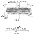
- Figure 5 presents a schematic overhead view of a CCD sampling circuit 10 embodying the apparatus and methods of the present invention.
- Figure 6 illustrates the same circuit in cross-section.
- Four sequentially sampling CCD injectors, 17a, 17b, 17c and 17d share a common ohmic contact 12 (the source of electron packets), sampling gate 14 and input gate 16.
- the cross-sectional view of Figure 6 represents a slice through injectors 17a and 17b.
- the entire device may be constructed on a single wafer of gallium arsenide (Ga As) along with drive circuitry and circuitry for further signal processing using techniques familiar to those skilled in the microelectronic arts.
- Ga As gallium arsenide
- the sampling gate 14 when high allows the surface potential under the input gate 16 in all four samplers 17a through 17d to equilibrate with the potential of the ohmic contact 12. When the sampling gate 14 goes low equal charges are isolated under the input gates 16 in the four samplers 17a through 17d.
- Each injector or charge output device 17 is further comprised of two CCD gates: a transfer gate 18, adjacent to one portion of the input signal gate 16, and a storage gate 20, adjacent to transfer gate 18. Charge packets move in localized channels outward from the sampling gate 14, to the input signal gate 16, and on to the transfer gate 18 and the storage gate 20.
- Each of the CCD gates described may be fabricated from a conductive layer separated from the semiconductor substrate by a thin dielectric layer (in the present embodiment, an aluminum conductive layer is separated from the Ga As substrate by a thin layer of silicon dioxide (SiO2)).
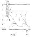
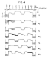
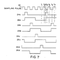
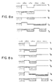
- the operation of the sampling circuit 10 may be understood by referring to Figures 5 and 6 in connection with the timing diagram shown in Figure 7 and the charge transfer diagrams revealed in Figures 8(a) and 8(b).
- the timing diagram of Figure 7 shows a clocked sampling pulse 22, which may be any uniform periodic waveform.
- the sampling pulse frequency determines the overall sampling rate of the circuit 10.
- the sampling frequency for the preferred embodiment here described is 4 gigahertz.
- the time-varying voltage of the sampling pulse 22 is applied to the sampling gate 14, uniformly varying the potential directly underneath the sampling gate electrode 14. When the sampling pulse's potential goes high, the Fermi level for electrons underneath the electrode 14 goes low, allowing a packet of electrons to flow underneath the sampling gate 14.
- the combination of the charge reservoir provided by ohmic contacts 12 and the sampling pulse 22 applied to the sampling gate 14 creates a steady and uniform supply of discrete charge packets to the sampling circuit 10.
- the potential of the sampling pulse 22 is low, the Fermi level underneath the sampling gate 14 (represented by Vsamp in Figures 8(a) and 8(b)) is high, and no charge flows from the reservoir underneath ohmic contacts 12 (Vohm).
- the sampling pulse 22 is high, the Fermi level of Vsamp is low, and charge flows across the sampling gate 14 to the input gate 16 (represented by Vin).
- the potential level of the input gate 16 determines how much charge flows across the sampling gate 14.
- the sampling pulse 22 is going low, the Fermi level of Vsamp is rising, and a discrete charge packet remains in the well underneath the input signal gate 16, Vin.
- the size of the charge packet which remains reflects accurately the instantaneous input voltage applied to the input gate 16.
- the charge packet is the same for all injectors 17 (seen by comparing the diagram for t3 in both Figures 8(a) and 8(b)).
- a single clock pulse 24a is applied to the transfer gate 18a of injector 17a, lowering the Fermi level under transfer gate 18a.
- a longer pulse 26a is simultaneously applied to storage gate 20a, also lowering its Fermi level.
- the two Fermi levels are shown as ⁇ 18a and ⁇ 20a in Figure 8(a). Because both Fermi levels have been driven low, the trapped charge underneath input signal gate 16 flows underneath transfer gate 18a and storage gate 20a. As the pulse 24a returns to its low value, causing the Fermi level underneath the transfer gate to again go high, the charge originally trapped underneath the input signal gate has now moved to and remains stored under storage gate 20a, whose Fermi level is still low and remains low for two full clock cycles.
- the sampling cycle has repeated itself and charge once again flows to the well located underneath input signal gate 16.
- the trapped charge under storage gate 20a is available for further transport away from the sampler circuit 10 and for measuring by any conventional means.
- the trapped charge at time t5 underneath storage gate 20a represents the instantaneous value of the input signal at time t3, when it was originally trapped.
- injector 17b for times t6 and t7 is exactly the same as for the corresponding times t4 and t5 for sampler 17a in Figure 8(a): the charge packet is transferred from the input signal gate 16 to sampler storage gate 20b. In likewise fashion, injectors 17c and 17d are "fired” in successive cycles, one injector gate each clock cycle. Since the overall sampling pulse 22 governs the interleaving of the separate injector gates 17, greater uniformity of interleaving results.
- Each data stream from a separate injector 17 comprises charge packets clocked at one fourth the sampling rate.
- the resulting rate reduction allows subsequent processing of each data stream at a much slower rate. It will be apparent that any number of injectors may be used in a given sampler circuit, to decimate the sampling of an input signal, further reducing the rate of each interleaved data stream. During subsequent processing, simply recombining the separate data streams regenerates the original signal.
Landscapes
- Solid State Image Pick-Up Elements (AREA)
Applications Claiming Priority (2)
| Application Number | Priority Date | Filing Date | Title |
|---|---|---|---|
| US375238 | 1989-06-30 | ||
| US07/375,238 US5015876A (en) | 1989-06-30 | 1989-06-30 | High speed charge-coupled sampler and rate reduction circuit |
Publications (2)
| Publication Number | Publication Date |
|---|---|
| EP0405210A2 true EP0405210A2 (de) | 1991-01-02 |
| EP0405210A3 EP0405210A3 (en) | 1991-06-12 |
Family
ID=23480084
Family Applications (1)
| Application Number | Title | Priority Date | Filing Date |
|---|---|---|---|
| EP19900110992 Withdrawn EP0405210A3 (en) | 1989-06-30 | 1990-06-11 | High speed charge-coupled sampler and rate reduction circuit |
Country Status (3)
| Country | Link |
|---|---|
| US (1) | US5015876A (de) |
| EP (1) | EP0405210A3 (de) |
| JP (1) | JPH0344942A (de) |
Families Citing this family (2)
| Publication number | Priority date | Publication date | Assignee | Title |
|---|---|---|---|---|
| US7733815B2 (en) * | 2006-07-28 | 2010-06-08 | Qimonda Ag | Data sampler including a first stage and a second stage |
| KR20200128109A (ko) * | 2018-03-02 | 2020-11-11 | 에이아이스톰, 아이엔씨. | 전하 도메인 수학적 엔진 및 방법 |
Family Cites Families (5)
| Publication number | Priority date | Publication date | Assignee | Title |
|---|---|---|---|---|
| FR2302636A1 (fr) * | 1975-02-28 | 1976-09-24 | Thomson Csf | Procede de filtrage de signaux analogiqu |
| US4099197A (en) * | 1976-08-12 | 1978-07-04 | Northern Telecom Limited | Complementary input structure for charge coupled device |
| US4210825A (en) * | 1976-12-08 | 1980-07-01 | Bell Telephone Laboratories, Incorporated | Linear differential charge splitting input for charge coupled devices |
| US4152606A (en) * | 1977-09-16 | 1979-05-01 | Hewlett-Packard Company | Waveform capture device |
| US4259598A (en) * | 1979-12-20 | 1981-03-31 | General Electric Company | Charge transfer signal processing apparatus transversal filter |
-
1989
- 1989-06-30 US US07/375,238 patent/US5015876A/en not_active Expired - Fee Related
-
1990
- 1990-06-11 EP EP19900110992 patent/EP0405210A3/en not_active Withdrawn
- 1990-06-29 JP JP2172572A patent/JPH0344942A/ja active Pending
Also Published As
| Publication number | Publication date |
|---|---|
| EP0405210A3 (en) | 1991-06-12 |
| US5015876A (en) | 1991-05-14 |
| JPH0344942A (ja) | 1991-02-26 |
Similar Documents
| Publication | Publication Date | Title |
|---|---|---|
| US4041298A (en) | Floating clock sensor for buffered, independent, non-destructive readout of charge transfer devices | |
| US4686648A (en) | Charge coupled device differencer | |
| US4156818A (en) | Operating circuitry for semiconductor charge coupled devices | |
| US4210825A (en) | Linear differential charge splitting input for charge coupled devices | |
| US4035667A (en) | Input circuit for inserting charge packets into a charge-transfer-device | |
| US3902186A (en) | Surface charge transistor devices | |
| US3935446A (en) | Apparatus for sensing radiation and providing electrical readout | |
| EP0324456A2 (de) | Ausgangsschaltung einer Ladungsschiebeanordnung | |
| USRE30087E (en) | Coherent sampled readout circuit and signal processor for a charge coupled device array | |
| US5015876A (en) | High speed charge-coupled sampler and rate reduction circuit | |
| US4627082A (en) | Semiconductor device for obtaining an accurate threshold voltage adjustment | |
| US4048525A (en) | Output circuit for charge transfer transversal filter | |
| US4152606A (en) | Waveform capture device | |
| US3790825A (en) | Gate-diffusion isolation for jfet depletion-mode bucket brigade circuit | |
| US5029189A (en) | Input structure for charge coupled devices with controllable input bias | |
| Tompsett | Using charge-coupled devices for analog delay | |
| US3906359A (en) | Magnetic field sensing CCD device with a slower output sampling rate than the transfer rate yielding an integration | |
| US3896484A (en) | Intrinsic semiconductor charge transfer device using alternate transfer of electrons and holes | |
| US4321584A (en) | Charge coupled digital-to-analog converter | |
| US4010484A (en) | Charge injection input network for semiconductor charge transfer device | |
| US4393357A (en) | High speed transient recorder systems | |
| US4028715A (en) | Use of floating diffusion for low-noise electrical inputs in CCD's | |
| US4194187A (en) | Analog-to-digital conversion by charge coupled device | |
| US4103109A (en) | Ccd multiplexer | |
| US3965368A (en) | Technique for reduction of electrical input noise in charge coupled devices |
Legal Events
| Date | Code | Title | Description |
|---|---|---|---|
| PUAI | Public reference made under article 153(3) epc to a published international application that has entered the european phase |
Free format text: ORIGINAL CODE: 0009012 |
|
| AK | Designated contracting states |
Kind code of ref document: A2 Designated state(s): DE FR GB IT NL |
|
| PUAL | Search report despatched |
Free format text: ORIGINAL CODE: 0009013 |
|
| AK | Designated contracting states |
Kind code of ref document: A3 Designated state(s): DE FR GB IT NL |
|
| STAA | Information on the status of an ep patent application or granted ep patent |
Free format text: STATUS: THE APPLICATION IS DEEMED TO BE WITHDRAWN |
|
| 18D | Application deemed to be withdrawn |
Effective date: 19911213 |