EP0404268B1 - Circuit for adapting the rates of two signals - Google Patents
Circuit for adapting the rates of two signals Download PDFInfo
- Publication number
- EP0404268B1 EP0404268B1 EP90201626A EP90201626A EP0404268B1 EP 0404268 B1 EP0404268 B1 EP 0404268B1 EP 90201626 A EP90201626 A EP 90201626A EP 90201626 A EP90201626 A EP 90201626A EP 0404268 B1 EP0404268 B1 EP 0404268B1
- Authority
- EP
- European Patent Office
- Prior art keywords
- bits
- clock
- signal
- bit
- circuit
- Prior art date
- Legal status (The legal status is an assumption and is not a legal conclusion. Google has not performed a legal analysis and makes no representation as to the accuracy of the status listed.)
- Expired - Lifetime
Links
Images


Classifications
-
- H—ELECTRICITY
- H04—ELECTRIC COMMUNICATION TECHNIQUE
- H04J—MULTIPLEX COMMUNICATION
- H04J3/00—Time-division multiplex systems
- H04J3/02—Details
- H04J3/06—Synchronising arrangements
- H04J3/07—Synchronising arrangements using pulse stuffing for systems with different or fluctuating information rates or bit rates
- H04J3/076—Bit and byte stuffing, e.g. SDH/PDH desynchronisers, bit-leaking
Definitions
- the invention relates to a circuit arrangement for adapting the bit rates of two signals.
- a first circuit arrangement is provided for inserting stuff bits and further information into a plesiochronous signal and a second circuit arrangement for removing stuff bits and the further information from the plesiochronous signal.
- Circuit arrangements of this type are required in message transmission, for example in the case of plesiochronous multiplexers, which bundle plesiochronous signals.
- Two binary signals are called plesiochronous if their bit rates are nominally the same, but can actually deviate from the nominal value within a given tolerance.
- plesiochronous signals Before plesiochronous signals can be combined by a plesiochronous multiplexer, they all have to be brought to the same bit rate, which (with so-called positive stuffing technology) is slightly higher than the bit rate that the individual plesiochronous signals have. This bit rate difference is compensated for, among other things, by including so-called stuff bits in the signal of higher bit rate from time to time.
- a circuit arrangement which, among other things, prepares and executes this process is the present arrangement.
- a corresponding circuit arrangement must be connected downstream of a plesiochronous demultiplexer in order to close the stuffing bits again remove and then bring the bitrate back to its original value.
- a circuit arrangement for adapting the bit rates of two binary signals with an elastic memory is e.g. known from DE 25 18 051 A1.
- a first address counter is clocked with the bit clock of the first and a second address counter with the (slightly changed) bit clock of the second signal.
- the address counters generate write and read addresses for an addressable buffer memory. The first signal is therefore read bit by bit into the buffer memory or read bit by bit from it again.
- a justification decision circuit which in the known arrangement consists of a phase comparator and a control circuit, compares write and read addresses of the counters and decides on the basis of the output signal of the phase comparator whether a clock edge is suppressed in the clock for the read counter and a stuff bit instead of the next bit in the buffer memory must be transferred.
- circuits in ECL technology have higher power losses than comparable circuits in CMOS technology. Circuits in CMOS technology, however, can only be used for frequencies up to about 80 MHz.
- the parallel bits have been formed from a serial first signal by means of a series-parallel converter.
- the bits buffered in the elastic memory are supplied to an additional memory and a switch.
- the changeover switch transmits certain bits directly from the elastic memory or the additional memory to a parallel-series converter to form a serial second signal.
- the changeover switch is set by a controller according to a darning criterion.
- the stuffing criterion can be obtained by evaluating the fill level of the elastic store or by comparing the phases. The switching status that was set last is only changed during a tamping process.
- the invention has for its object to further reduce the jitter generated by the known circuit arrangement.
- the circuit arrangement according to the invention also compares the phases of the write clock and the read clock with which the groups of parallel bits are written into and read from the elastic memory.
- the stuffing decision is made, which results in a reduction in jitter. It is important that the darning decision is always made at the same time interval from the darning point.
- dividers are included in the circuit arrangement.
- the dividers which have a division ratio of 1: n, are each provided for generating the write clock from the bit clock of the first signal and the read clock from the bit clock of the second signal.
- a phase comparator is provided for the phase comparison of the write clock and the read clock.
- the control device evaluates the output signal of the phase comparator when a predetermined edge occurs and sets the selection matrix for the insertion at least one stuffing bit if the fill level monitoring detects an excessive deviation from the setpoint.
- the selection matrix can be characterized by a track number s.
- the control device is provided to increase the number of tracks (s) by one unit modulo n per stuffing bit and to repeat the reading out of a group of bits from the elastic memory when the number of tracks s skips the value n-1.
- the predetermined edge is the m th edge relative to a reference edge in the reading cycle, where m results from the requirement, the amount of the expression m * TL / TS - k - s / n as a function of the integers m and k to be as small as possible, where TS and TL mean the period of the write clock and read clock, respectively.
- the elastic memory is an addressable buffer memory which is provided for receiving write addresses from a write counter received the write clock and read addresses from a read counter received the read clock.
- the fill level monitor serves to compare the write and read addresses and, in the event of a deviation from an address setpoint difference, to emit a signal to the control device.
- the control device is provided for regulating the address difference by changing the switching state of the selection matrix and by stopping the read counter.
- the selection matrix is coupled to a parallel-series converter for converting a group of n parallel bits into n serial bits of a second signal.
- a plesiochronous signal is obtained again from an STM-1 signal.
- dividers are provided, each having a divider ratio of 1: n and for generating the write clock from the Bit clock of the first signal and the read clock from the bit clock of the second signal serve.
- the phase locked loop in the circuit arrangement contains a phase comparator for phase comparison of the addresses supplied by a write counter and a read counter and for obtaining the bit clock for the second signal.
- the elastic memory is an addressable buffer memory which is provided for receiving write addresses from the write counter and read addresses from the read counter.
- the elastic memory is coupled to a parallel-series converter for converting a group of n parallel bits into n serial bits of a second signal.
- a first binary signal with a nominal bit rate of 139.264 Mbit / s is present at a terminal 1
- a second binary signal with a nominal bit rate structured according to frame is present at an output terminal 8 of 155.52 Mbit / s.
- the second binary signal contains stuff bits, stuff information bits and further auxiliary information.
- the framework is the so-called synchronous transport module STM-1 (compare e.g. the CCITT draft recommendations G 707, G 708 and G 709).
- the bit clock of the first signal is present at a terminal 10. This clock is reduced by a first divider 11 in a ratio of 1: 8.
- the reduced clock rate - hereinafter referred to as the write clock - has a pulse repetition frequency of 17.408 MHz.
- the integer variable n is to be chosen in the general teaching of 8.
- the write clock and the original bit clock are supplied to a series-parallel converter 2, which converts eight serial bits of the first signal into eight parallel bits, which are routed via lines 31 to 38 to eight read inputs of a buffer memory 4. Bits with the repetition frequency of 17.408 MHz are present on each of the lines 31 to 38, so that all components - with the exceptions made further below - which are to the right of the divider 11 and the series-parallel converter 2 in FIG CMOS technology are executed.
- a first address counter 12 - hereinafter referred to as write counter - is further developed, which cyclically generates write addresses for the eight-bit (one byte) wide buffer memory 4; the write clock is also passed to an input of a phase comparator 16. A different reduction of the bit clock is also possible for the phase comparator 16.
- the first signal is stored in bytes in the buffer memory 4 at a write address generated by the write counter 12.
- bit clock of the second binary signal which is present at a terminal 17, is passed to a second divider 14, which also divides this clock down by a ratio of 1: 8.
- This divided clock - hereinafter called reading clock - and the original bit clock clock a parallel-series converter 7, which converts the parallel processed first signal into the serial second signal with a bit rate of 155.52 Mbit / s and forwards it to an output terminal 8.
- All of the components that are to the left of the divider 14 and the parallel-serial converter 7 according to FIG. 1 are - with the exception of components 2 and 11 - implemented in low-loss CMOS technology, since they only process clock frequencies up to a maximum of 19.44 MHz to have.
- the read clock is used for the cyclical generation of read addresses by the address counter 13 and at the same time fed to a second input of the phase comparator 16 and a control unit 15.
- a fill level monitor 9 monitors the distance between write and read addresses and emits a characteristic signal to the control device 15 if this distance deviates too much from its target value. Half of the largest address is provided as the setpoint.
- the mode of operation of the circuit arrangement according to FIG. 1 would be easier to understand if all the auxiliary information could be transmitted byte by byte in the context of the second signal. In the present case, however, it is aggravated that some auxiliary information (frame header, for example) has to be inserted byte by byte, but the stuff bits only bit by bit.
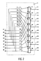
- the eight read outputs 41 to 48 (see FIG. 2) of the buffer memory 4 are connected to as many inputs of a selection matrix 5.
- Figure 2 shows an embodiment of such a selection matrix. It contains seven delay elements V1 to V7, which are connected to seven of their inputs 42 to 47. The delay elements V1 to V7 delay the bits at the inputs 42 to 47 of the selection matrix 5 by one clock period of the read clock. This results in a total of fifteen internal connection points Z1 to Z15 of the selection matrix.
- the selection matrix also contains eight 8: 1 selection circuits A1 to A8, the outputs of which are simultaneously the outputs 61 to 68 of the selection matrix 5.
- Each of the selection circuits A1 to A8 has eight inputs, each of which is connected to one of the connection points Z1 to Z15.
- the selection circuit A1 is connected to the connection points Z1 to Z8 (only the first and the last connection are shown in FIG.
- the second selection circuit is connected to the connection points Z2 to Z9 etc. up to the selection circuit A8 which is connected to the Connection points Z8 to Z15 is connected.
- the selection circuits A1 to A8 connect - controlled by addresses - one of their inputs to their output.
- the control lines for the selection circuits A1 to A8 and clock supply lines are not shown in FIG. 2.
- the table according to FIG. 3 serves to explain the mode of operation of the selection matrix according to FIG. 2.
- the table according to FIG. 3 contains the connection points Z1 to Z15 in its left margin column.
- the top line shows numbers of clock periods of the reading clock, which are also used as column numbers.
- Column 1 shows the data that are present at terminals Z1 to Z15 during a first read clock period; these are bits a1 to a8 of the first byte read.
- the double border indicates that the bits of the first bytes in the order from top to bottom, in this case in the order a1 to a8, are passed on to the output lines 61 to 68 of the selection matrix 5 by appropriate setting of the selection circuits A1 to A8.
- This repeated bit is forwarded on line 61 and can remain unchanged if its value is not important (eg stuffing bit); otherwise it must be overwritten by a circuit arrangement, not shown, with a very specific value.
- bits C1 to C8 of a new byte appear at the terminals Z8 to Z15, whereas bits b2 to b8 of the previous byte are present at the terminals Z1 to Z7.
- the double-bordered part in the third column shows that the first bit is the bit b8 of the second byte, which was not transmitted in the previous reading cycle, is now transferred to line 61.
- the underlining of bit a8 means that the information transmitted by it is already known to the recipient and can therefore be overwritten if such an overwriting is necessary.
- FIG. 3 shows that the track number s can assume a total of eight different integer values. If the number of tracks is selected so that it receives the value 0 in the switching state according to column 1 and progressively runs through all the integer values until the switching state according to column 7, the number of tracks s simultaneously indicates the number of modulo 8 stuffing bits transmitted. If the number of tracks skips the number 7, as in the transition from column 7 to column 8 of FIG. 3, the read counter and the delay elements V1 to V7 are stopped for one cycle and in the example according to FIG. 3 the seventh byte is read out again, so that none Information is lost.
- the control circuit 15 thus sets the switching state of the switching matrix 5 by counting the additional bits to be transmitted with a track number counter modulo 8 and by giving control addresses for the selection circuits A1 to A8 in accordance with the status s of this counter.
- the distance criterion of the write and read addresses has priority over all other criteria. If the distance deviates from its setpoint, stuffing bits are inserted until the setpoint distance is reached. Because of the structure of the frame, only one bit per frame line can be stuffed, so that - mostly when the arrangement is started up - a very long stuffing has to be done. In this case, the track number counter continuously and cyclically runs through all values from zero to seven. When the jump from seven to zero - compare the table in FIG. 3 - the read counter 13 and the delay elements V1 to V7 are stopped for one clock. The control circuit 15 also takes over the stopping of the read counter 13.
- Another criterion for increasing the number of tracks is the frequency difference between the write and read clock or the bit clock of the first signal and the bit clock of the second signal. With the aid of the phase comparator 16 and the control circuit 15, a decision is made as to whether or not to stuff because of this difference.
- the phase comparator 16 alone only compares the write and read clock and continuously outputs the result of this comparison to the control device 15. If the phase comparator 16 signals that stuffing is to take place - in other words, if there is a flank of the reading clock from the corresponding flank of the slower writing clock - then if a bit is really stuffed, the reading clock should be stopped for the duration of a bit (on the Timeline shifted) so that the distance is shortened accordingly and incorrect decisions are not made due to the absence of the shortening. Stopping the reading pulse for the duration of one bit (of the second signal) would, however, again require fast components which the circuit just avoided should be. Therefore there is no shifting of the reading pulse; Which equivalent measures are taken as an alternative can be found in the explanations below. Before doing so, however, one aspect of jitter in the recovered first signal on the receiver side will be discussed.
- bits may only be stuffed at a certain point in the frame lines.
- the recipient is informed by the stuffing information bits mentioned above whether the bit at the stuffing point is a stuffing bit or an information bit. For this reason, the decision whether to stop or not (darning decision) must be made on the order of a frame length in front of the darning point. If the time of this decision randomly fluctuates relative to the frame, this results in an additional jitter, the so-called waiting time jitter (see: Duttweiler, DL: Waiting Time Jitter. Bell Syst. Tech. J. 51, (1972), page 165 to 207). It is therefore desirable that the decision whether to insert a stuff bit or an information bit at the stuffing point is always made at the same time interval before this point.
- this additional jitter (waiting time jitter) is avoided, however, by systematically varying the point in time that is decisive for the stuffing decision. This variation is based on the following considerations:
- edges can be specified in it, each at a sufficient distance from the Darning points are located and are always at the same distance from them.
- These edges - hereinafter referred to as reference edges - are recognized by the control unit 15 (by counting the edges with the beginning of a line), which evaluates the output signal of the phase comparator 16 when the m th edge occurs relative to a reference edge, that is, at this point in time he sign of the phase position of the writing cycle to the (undisplaced) reading cycle and the knowledge of this sign makes the darning decision.
- the integer m searched for results from the requirement that the amount of the expression m * TL / TS - k - s / 8 as a function of the integers m and k should be as small as possible.
- TL means the period of the reading cycle
- TS the period of the writing cycle
- s the number of tracks mentioned above.
- the requirement itself can be derived from a consideration of the phase difference between the write clock and a read clock shifted by s bit at the time of a reference edge.
- the division of the track number s by 8 is related to the reduction of the bit clocks in a ratio of 1: 8. In the case of a generalization, this 8 must be replaced by n.
- the range of the permitted m and k values is to be selected such that the expression given can be made sufficiently small for all s from zero to seven, since it is a measure of the phase error which the present arrangement makes compared to an arrangement, in which the bit numbers are compared.
- the m (s) determined in this way is stored in a memory of the control circuit 15, which is also implemented only in CMOS technology.
- the track number s thus determines the edge of the reading pulse at which the phase comparator 16 is queried and the switching state of the selection matrix 5.
- an incoming binary signal arriving at a terminal 41 is fed to a series-parallel converter 42 on the receiver side of a transmission system.
- This first binary signal has a nominal bit rate of 155.52 Mbit / s and is one of four STM-1 signals which result after a STM-4 signal has been broken down by a demultiplexer, not shown.
- the arrangement according to FIG. 4 is supplied with the bit clock of the first binary signal provided with clock gaps via a terminal 410 and the stuffing information bits obtained from the first binary signal via a terminal 418.
- the stuffing information bits and the clocked bit clock are obtained from the transmitted STM-4 signal by an arrangement, not shown, associated with the demultiplexer.
- Terminal 418 is connected to a control device 415, which essentially consists of a cyclically running track number counter, with the aid of which the switching state of a selection matrix 45 is set.
- the track number counter is clocked with the byte clock which results from the bit clock of the first binary signal after division in a ratio of 1: 8 by a divider 411.
- the gaps in the bit clock at terminal 410 are distributed in such a way that after the clock is reduced at the output of divider 411, there is a byte clock with byte clock gaps.
- the Control device 415 For orientation in the current frame of the first binary signal, the Control device 415 the necessary information supplied via a terminal 419. The unit that supplies this information is also assigned to the demultiplexer.
- the selection matrix 45 is constructed according to the same principle as the selection matrix 5 in FIGS. 1 and 2.
- the first binary signal is transferred from the series-parallel converter 42 to the selection matrix 45 on lines 431 to 438. Controlled by a write counter 412, which is clocked by the gapped byte clock, the first binary signal is then written into a buffer memory 44 byte by byte without stuffing bytes.
- a read counter 413 controls the byte-by-byte readout from the buffer memory 44. The bytes read out are forwarded via lines 461 to 468 to a parallel-series converter 47, at the output 48 of which the second binary signal with a nominal bit rate of 139.264 Mbit / s is present.
- a phase comparator 49 is part of a phase-locked loop, not shown, with the aid of which the (gapless) bit clock of the second binary signal is obtained. This bit clock is present at terminal 417. It is divided down by a divider 414 in a 1: 8 ratio.
- the read counter 413 is supplied with the divided clock and the parallel-series converter 47 with the divided and undivided clock
Description
Die Erfindung betrifft eine Schaltungsanordnung zur Anpassung der Bitraten zweier Signale. Eine erste Schaltungsanordnung ist dabei zur Einfügung von Stopfbits und weiteren Informationen in ein plesiochrones Signal und eine zweite Schaltungsanordnung zum Entfernen von Stopfbits und den weiteren Informationen aus dem plesiochronen Signal vorgesehen.The invention relates to a circuit arrangement for adapting the bit rates of two signals. A first circuit arrangement is provided for inserting stuff bits and further information into a plesiochronous signal and a second circuit arrangement for removing stuff bits and the further information from the plesiochronous signal.
Derartige Schaltungsanordnungen werden in der Nachrichtenübertragung z.B. bei plesiochronen Multiplexern benötigt, die plesiochrone Signale bündeln. Zwei binäre Signale heißen plesiochron, wenn ihre Bitraten nominell gleich sind, tatsächlich aber innerhalb einer gegebenen Toleranz vom Nennwert abweichen können. Bevor plesiochrone Signale durch einen plesiochronen Multiplexer zusammengefaßt werden können, müssen sie alle auf die gleiche Bitrate gebracht werden, die (bei sogenannter positiver Stopftechnik) etwas höher liegt als die Bitrate, die die einzelnen plesiochronen Signale haben. Dieser Bitratenunterschied wird u.a. dadurch ausgeglichen, daß in das Signal höherer Bitrate von Zeit zu Zeit zusätzlich sogenannte Stopfbits aufgenommen werden. Eine Schaltungsanordnung, die unter anderem diesen Vorgang vorbereitet und durchführbar macht, ist die vorliegende Anordnung. Eine entsprechende Schaltungsanordnung ist einem plesiochronen Demultiplexer nachzuschalten, um die Stopfbits wieder zu entfernen und dann die Bitrate auf ihren ursprünglichen Wert zu bringen.Circuit arrangements of this type are required in message transmission, for example in the case of plesiochronous multiplexers, which bundle plesiochronous signals. Two binary signals are called plesiochronous if their bit rates are nominally the same, but can actually deviate from the nominal value within a given tolerance. Before plesiochronous signals can be combined by a plesiochronous multiplexer, they all have to be brought to the same bit rate, which (with so-called positive stuffing technology) is slightly higher than the bit rate that the individual plesiochronous signals have. This bit rate difference is compensated for, among other things, by including so-called stuff bits in the signal of higher bit rate from time to time. A circuit arrangement which, among other things, prepares and executes this process is the present arrangement. A corresponding circuit arrangement must be connected downstream of a plesiochronous demultiplexer in order to close the stuffing bits again remove and then bring the bitrate back to its original value.
Eine Schaltungsanordnung zur Anpassung der Bitraten zweier binärer Signale mit einem elastischen Speicher ist z.B. aus der DE 25 18 051 A1 bekannt. Bei dieser Anordnung wird ein erster Adreßzähler mit dem Bittakt des ersten und ein zweiter Adreßzähler mit dem (leicht veränderten) Bittakt des zweiten Signales getaktet. Die Adreßzähler erzeugen Schreib- und Leseadressen für einen adressierbaren Pufferspeicher. Das erste Signal wird daher bitweise in den Pufferspeicher eingelesen bzw. bitweise aus ihm wieder ausgelesen. Eine Stopfentscheidungsschaltung, die bei der bekannten Anordnung aus einem Phasenvergleicher und einer Steuerschaltung besteht, vergleicht Schreib- und Leseadressen der Zähler und entscheidet anhand des Ausgangssignals des Phasenvergleichers, ob in dem Takt für den Lesezähler eine Taktflanke unterdrückt und statt des nächstfolgenden Bits im Pufferspeicher ein Stopfbit übertragen werden muß.A circuit arrangement for adapting the bit rates of two binary signals with an elastic memory is e.g. known from
Soll die bekannte Schaltungsanordnung für Bitraten in der Größenordnung von 140 Mbit/s und darüber eingesetzt werden, so muß sie in ECL-Technologie ausgeführt werden. Bei Schaltungen in ECL-Technologie treten jedoch höhere Verlustleistungen auf als bei vergleichbaren Schaltungen in CMOS-Technologie. Schaltungen in CMOS-Technologie sind dagegen nur für Frequenzen bis etwa 80 MHz brauchbar.If the known circuit arrangement is to be used for bit rates in the order of magnitude of 140 Mbit / s and above, it must be implemented in ECL technology. Circuits in ECL technology, however, have higher power losses than comparable circuits in CMOS technology. Circuits in CMOS technology, however, can only be used for frequencies up to about 80 MHz.
Eine Schaltungsanordnung zur Taktanpassung in der digitalen Nachrichtentechnik, die für Bitraten in der Größenordnung von 140 Mbit/s verwendet werden kann, jedoch nur wenige Bausteine in ECL-Technologie benötigt, ist aus der nicht vorveröffentlichten EP-0 374 436 A2 bekannt.A circuit arrangement for clock adaptation in digital communications technology, which can be used for bit rates in the order of magnitude of 140 Mbit / s, but only requires a few components in ECL technology, is known from the unpublished EP-0 374 436 A2.
Diese enthält einen elastischen Speicher, dem 4 pararllele Bits jeweils zugeführt werden. Die parallelen Bits sind mittels eines Serien-Parallel-Wandlers aus einem seriellen ersten Signal gebildet worden. Die in dem elastischen Speicher gepufferten Bits werden einem Zusatzspeicher und einem Umschalter geliefert. Der Umschalter gibt jeweils abhängig von seiner Schaltstellung bestimmte Bits direkt von dem elastischen Speicher oder dem Zusatzspeicher an einen Parallel-Serien-Wandler zur Bildung eines seriellen zweiten Signals. Der Umschalter wird von einer Steuerung entsprechend einem Stopfkriterium eingestellt. Das Stopfkriterium kann durch Auswerten des Füllstandes des elastischen Speichers oder durch einen Phasenvergleich gewonnen werden. Es wird also nur bei einem Stopfvorgang der zuletzt eingestellte Schaltzustand verändert.This contains an elastic memory, to which 4 parallel bits are fed. The parallel bits have been formed from a serial first signal by means of a series-parallel converter. The bits buffered in the elastic memory are supplied to an additional memory and a switch. Depending on its switching position, the changeover switch transmits certain bits directly from the elastic memory or the additional memory to a parallel-series converter to form a serial second signal. The changeover switch is set by a controller according to a darning criterion. The stuffing criterion can be obtained by evaluating the fill level of the elastic store or by comparing the phases. The switching status that was set last is only changed during a tamping process.
Der Erfindung liegt die Aufgabe zugrunde, den von der bekannten Schaltungsanordnung erzeugten Jitter weiter zu reduzieren.The invention has for its object to further reduce the jitter generated by the known circuit arrangement.
Diese Aufgabe wird durch eine Schaltungsanordung zur Anpassung der Bitraten zweier Signale mit folgenden Merkmalen gelöst:
Die Schaltungsanordnung enthält
- einen Serien-Parallel-Wandler zur Wandlung von jeweils n seriellen Bits eines ersten Signals in eine Gruppe von n parallelen Bits,
- einen elastischen Speicher zum jeweiligen Einschreiben und zum jeweiligen Auslesen einer Gruppe von parallelen Bits,
- eine ein zweites Signal liefernde Auswahlmatrix, die bei einem Stopfvorgang zur Verzögerung bestimmter Bits von aufeinanderfolgenden Gruppen paralleler Bits und zur Einfügung von Stopfbits anstelle der bestimmten Bits vorgesehen ist, und
- eine Steuervorrichtung zur Steuerung des Auslesevorgangs aus dem elastischen Speicher und der Auswahlmatrix in Abhängigkeit von einem Phasenvergleich eines Schreibtaktes und eines Lesetaktes zu einem immer im gleichen zeitlichen Abstand von einer Stopfstelle liegenden Zeitpunkt und einer Füllstandsüberwachung des elastischen Speichers.
The circuit arrangement contains
- a series-parallel converter for converting in each case n serial bits of a first signal into a group of n parallel bits,
- an elastic memory for writing in and reading out a group of parallel bits,
- a selection matrix providing a second signal which, in the case of a stuffing process, is used to delay certain bits of successive groups of parallel bits and to insert stuff bits instead of certain bits is provided, and
- a control device for controlling the readout process from the elastic memory and the selection matrix as a function of a phase comparison of a write cycle and a read cycle at a time which is always at the same time interval from a darning point and a fill level monitoring of the elastic memory.
Die erfindungsgemäße Schaltungsanordnung vergleicht noch miteinander die Phasen des Schreibtaktes und des Lesetaktes, mit dem die Gruppen von parallelen Bits in den elastischen Speicher eingeschrieben und ausgelesen werden.The circuit arrangement according to the invention also compares the phases of the write clock and the read clock with which the groups of parallel bits are written into and read from the elastic memory.
In Abhängigkeit von der Phasenlage wird die Stopfentscheidung getroffen, wodurch sich eine Reduzierung des Jitters ergibt. Hierbei ist wichtig, daß die Stopfentscheidung immer im gleichen zeitlichen Abstand von der Stopfstelle getroffen wird.Depending on the phase position, the stuffing decision is made, which results in a reduction in jitter. It is important that the darning decision is always made at the same time interval from the darning point.
Zur Erzeugung des Schreib- und Lesetaktes sind Teiler in der Schaltungsanordnung enthalten. Die Teiler, die ein Teilerverhältnis von 1:n aufweisen, sind jeweils zur Erzeugung des Schreibtaktes aus dem Bittakt des ersten Signals und des Lesetaktes aus dem Bittakt des zweiten Signals vorgesehen.To generate the write and read clock, dividers are included in the circuit arrangement. The dividers, which have a division ratio of 1: n, are each provided for generating the write clock from the bit clock of the first signal and the read clock from the bit clock of the second signal.
Ein Phasenvergleicher ist zum Phasenvergleich des Schreibtaktes und des Lesetaktes vorgesehen. Die Steuervorrichtung wertet das Ausgangssignal des Phasenvergleichers beim Auftreten einer vorbestimmten Flanke aus und stellt die Auswahlmatrix für die Einfügung wenigstens eines Stopfbits ein, wenn die Füllstandsüberwachung ein zu starkes Abweichen vom Sollwert feststellt.A phase comparator is provided for the phase comparison of the write clock and the read clock. The control device evaluates the output signal of the phase comparator when a predetermined edge occurs and sets the selection matrix for the insertion at least one stuffing bit if the fill level monitoring detects an excessive deviation from the setpoint.
Die Auswahlmatrix kann durch eine Spurzahl s charakterisiert werden. Die Steuervorrichtung ist zur Erhöhung der Spurzahl (s) um eine Einheit Modulo n pro Stopfbit und zur Wiederholung des Auslesens einer Bitgruppe aus dem elastischen Speicher vorgesehen, wenn die Spurzahl s den Wert n - 1 überspringt.The selection matrix can be characterized by a track number s. The control device is provided to increase the number of tracks (s) by one unit modulo n per stuffing bit and to repeat the reading out of a group of bits from the elastic memory when the number of tracks s skips the value n-1.
Die vorbestimmte Flanke ist die m-te Flanke relativ zu einer Bezugsflanke im Lesetakt, wobei sich m aus der Forderung ergibt, den Betrag des Ausdrucks![]()
![]()
Bei dem elastischen Speicher handelt es sich um einen adressierbaren Pufferspeicher, der zum Empfang von Schreibadressen von einem den Schreibtakt erhaltenen Schreibzähler und von Leseadressen von einem den Lesetakt erhaltenen Lesezähler vorgesehen ist.The elastic memory is an addressable buffer memory which is provided for receiving write addresses from a write counter received the write clock and read addresses from a read counter received the read clock.
Die Füllstandsüberwachung dient zum Vergleich der Schreib- und Leseadressen und bei Abweichung von einer Adressensolldifferenz zur Abgabe eines Signals an die Steuervorrichtung. Die Steuervorrichtung ist zur Regelung der Adressendifferenz durch eine Veränderung des Schaltzustandes der Auswahlmatrix und durch ein Anhalten des Lesezählers vorgesehen.The fill level monitor serves to compare the write and read addresses and, in the event of a deviation from an address setpoint difference, to emit a signal to the control device. The control device is provided for regulating the address difference by changing the switching state of the selection matrix and by stopping the read counter.
Die Auswahlmatrix ist mit einem Parallel-Serien-Wandler zur Wandlung von jeweils einer Gruppe von n parallen Bits in jeweils n serielle Bits eines zweiten Signals gekoppelt.The selection matrix is coupled to a parallel-series converter for converting a group of n parallel bits into n serial bits of a second signal.
Die Erfindung bezieht sich auch auf eine Schaltungsanordnung zur Anpassung der Bitraten zweier Signale mit
- einem Serien-Parallel-Wandler zur Wandlung von jeweils n seriellen Bits eines ersten Signals in eine Gruppe von n parallelen Bits,
- einer Auswahlmatrix, die bei einem Entstopfvorgang zur Verzögerung bestimmter Bits von aufeinanderfolgenden Gruppen paralleler Bits des ersten Signals und zur Weiterleitung von Gruppen paralleler Bits mit Ausnahme der Stopfbits vorgesehen ist,
- einem elastischen Speicher zum jeweiligen Einschreiben einer von der Auswahlmatrix gelieferten Gruppe von parallelen Bits und zum jeweiligen Auslesen einer Gruppe von parallelen Bits für ein zweites Signal,
- einer Steuervorrichtung zum Empfang von Stopfinformationsbits und zur Steuerung der Auswahlmatrix und
- einer Phasenregelschleife zur Steuerung des Ausschreibens der Bits aus dem elastischen Speicher.
- a series-parallel converter for converting n serial bits of a first signal into a group of n parallel bits,
- a selection matrix which is provided in a de-stuffing process to delay certain bits of successive groups of parallel bits of the first signal and to forward groups of parallel bits with the exception of the stuff bits,
- an elastic memory for writing in a group of parallel bits supplied by the selection matrix and for reading out a group of parallel bits for a second signal,
- a control device for receiving stuffing information bits and for controlling the selection matrix and
- a phase locked loop for controlling the writing out of the bits from the elastic memory.
In dieser Schaltungsanordnung wird beispielsweise aus einem STM-1-Signal wieder ein plesiochrones Signal gewonnen.In this circuit arrangement, for example, a plesiochronous signal is obtained again from an STM-1 signal.
Zur Erzeugung eines Schreib- und Lesetaktes sind Teiler vorgesehen, die jeweils ein Teilerverhältnis von 1:n aufweisen und zur Erzeugung des Schreibtaktes aus dem Bittakt des ersten Signals und des Lesetaktes aus dem Bittakt des zweiten Signals dienen.To generate a write and read clock, dividers are provided, each having a divider ratio of 1: n and for generating the write clock from the Bit clock of the first signal and the read clock from the bit clock of the second signal serve.
Die Phasenregelschleife in der Schaltungsanordnung enthält einen Phasenvergleicher zum Phasenvergleich der von einem Schreibzähler und einem Lesezähler gelieferten Adressen und zur Gewinnung des Bittaktes für das zweite Signal.The phase locked loop in the circuit arrangement contains a phase comparator for phase comparison of the addresses supplied by a write counter and a read counter and for obtaining the bit clock for the second signal.
Bei dem dem elastischen Speicher handelt es sich um einen adressierbaren Pufferspeicher, der zum Empfang von Schreibadressen von dem Schreibzähler und von Leseadressen von dem Lesezähler vorgesehen ist. Der elastische Speicher ist mit einem Parallel-Serien-Wandler zur Wandlung von jeweils einer Gruppe von n parallen Bits in jeweils n serielle Bits eines zweiten Signals gekoppelt.The elastic memory is an addressable buffer memory which is provided for receiving write addresses from the write counter and read addresses from the read counter. The elastic memory is coupled to a parallel-series converter for converting a group of n parallel bits into n serial bits of a second signal.
Anhand der Figuren und anhand eines Ausführungsbeispiels für einen plesiochronen Multiplexer und einen plesiochronen Demultiplexer soll die Erfindung näher erläutert werden.The invention will be explained in more detail with reference to the figures and using an exemplary embodiment for a plesiochronous multiplexer and a plesiochronous demultiplexer.
Es zeigt:
- Fig. 1 ein Prinzipschaltbild der erfindungsgemäßen Anordnung für einen plesiochronen Multiplexer,
- Fig. 2 eine Auswahlmatrix,
- Fig. 3 eine Tabelle zur Funktionserläuterung der Auswahlmatrix und
- Fig. 4 ein Prinzipschaltbild der erfindungsgemäßen Anordnung für einen plesiochronen Demultiplexer.
- 1 shows a basic circuit diagram of the arrangement according to the invention for a plesiochronous multiplexer,
- 2 shows a selection matrix,
- Fig. 3 is a table for explaining the function of the selection matrix and
- Fig. 4 is a schematic diagram of the arrangement according to the invention for a plesiochronous demultiplexer.
In Figur 1 liegt an einer Klemme 1 ein erstes binäres Signal mit einer nominellen Bitrate von 139,264 Mbit/s an, und an einer Ausgangsklemme 8 ein nach Rahmen strukturiertes zweites binäres Signal mit einer nominellen Bitrate von 155,52 Mbit/s. Das zweite Binärsignal enthält neben sämtlichen Bits des ersten Signals Stopfbits, Stopfinformationsbits sowie weitere Hilfsinformationen.In FIG. 1, a first binary signal with a nominal bit rate of 139.264 Mbit / s is present at a
Der Rahmen ist der sogenannte synchrone Transportmodul STM-1 (vergleiche hierzu z.B. die CCITT-Empfehlungsentwürfe G 707, G 708 und G 709).The framework is the so-called synchronous transport module STM-1 (compare e.g. the CCITT draft recommendations G 707, G 708 and G 709).
An einer Klemme 10 liegt der Bittakt des ersten Signales an. Dieser Takt wird durch einen ersten Teiler 11 im Verhältnis 1:8 untersetzt. Der untersetzte Takt - nachfolgend Schreibtakt genannt - hat eine Impulsfolgefrequenz von 17,408 MHz. Im vorliegenden Beispiel ist also die ganzzahlige Variable n in der allgemeinen Lehre zu 8 zu wählen.The bit clock of the first signal is present at a terminal 10. This clock is reduced by a
Mit dem Schreibtakt und dem ursprünglichen Bittakt wird ein Serien-Parallel-Wandler 2 versorgt, der acht serielle Bits des ersten Signales in acht parallele Bits umwandelt, die über Leitungen 31 bis 38 an acht Leseeingänge eines Pufferspeichers 4 geführt werden. Auf jeder der Leitungen 31 bis 38 liegen Bits mit der Folgefrequenz von 17,408 MHz an, so daß alle Bausteine - bis auf die weiter unten gemachten Ausnahmen - die in Figur 1 rechts vom Teiler 11 und dem Serien-Parallel-Wandler 2 liegen, in verlustarmer CMOS-Technologie ausgeführt sind. Mit dem Schreibtakt wird ein erster Adreßzähler 12 - im folgenden Schreibzähler genannt - weitergestellt, der zyklisch Schreibadressen für den acht Bit (ein Byte) breiten Pufferspeicher 4 erzeugt; der Schreibtakt wird auch an einen Eingang eines Phasenvergleichers 16 geleitet. Für den Phasenvergleicher 16 ist jedoch auch eine andere Untersetzung des Bittaktes möglich. Unter einer vom Schreibzähler 12 erzeugten Schreibadresse wird das erste Signal byteweise im Pufferspeicher 4 abgelegt.The write clock and the original bit clock are supplied to a series-
Der Bittakt des zweiten Binärsignales, der an einer Klemme 17 anliegt, wird an einen zweiten Teiler 14 geleitet, der diesen Takt ebenfalls im Verhältnis 1:8 herunterteilt.The bit clock of the second binary signal, which is present at a terminal 17, is passed to a
Dieser geteilte Takt - nachfolgend Lesetakt genannt - und der ursprüngliche Bittakt takten einen Parallel-Serien-Wandler 7, der das parallel verarbeitete erste Signal in das serielle zweite Signal mit einer Bitrate von 155,52 Mbit/s wandelt und an eine Ausgangsklemme 8 weiterleitet. Alle Bausteine, die nach Figur 1 links vom Teiler 14 und vom Parallel-Seriell-Wandler 7 liegen, sind - bis auf die Bausteine 2 und 11 - in verlustarmer CMOS-Technologie ausgeführt, da sie nur Taktfrequenzen bis maximal 19,44 MHz zu verarbeiten haben.This divided clock - hereinafter called reading clock - and the original bit clock clock a parallel-
Der Lesetakt wird zur zyklischen Erzeugung von Leseadressen durch den Adreßzähler 13 verwendet und gleichzeitig einem zweiten Eingang des Phasenvergleichers 16 und einer Steuereinheit 15 zugeführt.The read clock is used for the cyclical generation of read addresses by the
Eine Füllstandsüberwachung 9 überwacht den Abstand von Schreib- und Leseadressen und gibt ein charakteristisches Signal an die Steuervorrichtung 15 ab, wenn dieser Abstand zu sehr von seinem Sollwert abweicht. Als Sollwert ist die Hälfte der größten Adresse vorgesehen.A fill level monitor 9 monitors the distance between write and read addresses and emits a characteristic signal to the
Die Funktionsweise der Schaltungsanordnung nach Figur 1 wäre leichter verständlich, wenn im Rahmen des zweiten Signales alle Hilfsinformationen byteweise übertragen werden könnten. Im vorliegenden Fall ist jedoch erschwerend, daß manche Hilfsinformation (Rahmenkopf zum Beispiel) byteweise eingefügt werden müssen, die Stopfbits jedoch nur bitweise. Um einzelne Bits oder Bytes in das zweite Signal einfügen zu können, sind die acht Leseausgänge 41 bis 48 (vergleiche Figur 2) des Pufferspeichers 4 mit ebensovielen Eingängen einer Auswahlmatrix 5 verbunden.The mode of operation of the circuit arrangement according to FIG. 1 would be easier to understand if all the auxiliary information could be transmitted byte by byte in the context of the second signal. In the present case, however, it is aggravated that some auxiliary information (frame header, for example) has to be inserted byte by byte, but the stuff bits only bit by bit. In order to be able to insert individual bits or bytes into the second signal, the eight read
Figur 2 zeigt ein Ausführungsbeispiel einer solchen Auswahlmatrix. Sie enthält sieben Verzögerungsglieder V1 bis V7, die mit sieben ihrer Eingänge 42 bis 47 verbunden sind. Die Verzögerungsglieder V1 bis V7 verzögern die Bits an den Eingängen 42 bis 47 der Auswahlmatrix 5 um eine Taktperiode des Lesetaktes. Insgesamt ergeben sich auf diese Weise fünfzehn interne Anschlußpunkte Z1 bis Z15 der Auswahlmatrix. Des weiteren enthält die Auswahlmatrix acht 8:1-Auswahlschaltungen A1 bis A8, deren Ausgänge gleichzeitig die Ausgänge 61 bis 68 der Auswahlmatrix 5 sind. Jede der Auswahlschaltungen A1 bis A8 hat acht Eingänge, von denen jeder mit einem der Anschlußpunkte Z1 bis Z15 verbunden ist. Im einzelnen gilt, daß die Auswahlschaltung A1 mit den Anschlußpunkten Z1 bis Z8 verbunden ist (nur die erste und die letzte Verbindung sind in Figur 2 eingezeichnet), die zweite Auswahlschaltung mit den Anschlußpunkten Z2 bis Z9 usw. bis zur Auswahlschaltung A8, die mit den Anschlußpunkten Z8 bis Z15 verbunden ist. Die Auswahlschaltungen A1 bis A8 verbinden - gesteuert durch Adressen - einen ihrer Eingänge mit ihrem Ausgang. Die Steuerleitungen für die Auswahlschaltungen A1 bis A8 und Taktversorgungsleitungen sind in Figur 2 nicht eingetragen.Figure 2 shows an embodiment of such a selection matrix. It contains seven delay elements V1 to V7, which are connected to seven of their
Fig. 3 dient der Erläuterung der Funktionsweise der Auswahlmatrix nach Fig. 2. Die Tabelle nach Fig. 3 enthält in ihrer linken Randspalte die Anschlußpunkte Z1 bis Z15. In der obersten Zeile sind Nummern von Taktperioden des Lesetaktes angegeben, die gleichzeitig als Spaltennummern verwendet werden. Insgesamt wird die Funktionsweise der Auswahlmatrix 5 anhand der Ereignisse von 10 Taktperioden des Lesetaktes demonstriert. In Spalte 1 sind die Daten angegeben, die während einer ersten Lesetaktperiode an den Anschlußklemmen Z1 bis Z15 anliegen; es sind dies die Bits a1 bis a8 des ersten ausgelesenen Bytes. Die doppelte Umrandung deutet an, daß die Bits des ersten Bytes in der Reihenfolge von oben nach unten, also hier in der Reihenfolge a1 bis a8, durch entsprechende Einstellung der Auswahlschaltungen A1 bis A8 auf die Ausgangsleitungen 61 bis 68 der Auswahlmatrix 5 weitergegeben werden. In der zweiten Taktperiode liegen - wie die Spalte 2 der Fig. 3 zeigt - die Bits b1 bis b8 des zweiten Bytes an den Anschlußklemmen Z8 bis Z15 an, während die Bits a2 bis a8 des vorangegangenen Bytes an den Anschlußpunkten Z1 bis Z7 anliegen. Der doppelt umrandete Teil in der Spalte 2 läßt wieder den Schaltzustand der Auswahlschaltungen A1 bis A8 erkennen. Jetzt werden die Anschlußpunkte Z7 bis Z14 mit den Leitungen 61 bis 68 verbunden. Erkennbar ist auch, daß vom zweiten Byte die Bits b1 bis b7 übertragen werden und das achte Bit a8 des vorangegangenen Bytes wiederholt wird. Dieses wiederholte Bit wird auf der Leitung 61 weitergeleitet und kann, wenn es auf seinen Wert nicht ankommt (z.B. Stopfbit), unverändert bleiben; andernfalls muß es von einer nicht gezeigten Schaltungsanordnung mit einem ganz bestimmten Wert überschrieben werden. In der dritten Taktperiode des Lesetaktes erscheinen die Bits C1 bis C8 eines neuen Bytes an den Anschlußklemmen Z8 bis Z15, wogegen die Bits b2 bis b8 des vorangegangenen Bytes an den Anschlußklemmen Z1 bis Z7 anliegen. Der doppelt umrandete Teil in der dritten Spalte läßt erkennen, daß als erstes Bit das im vorangegangenen Lesetakt nicht übertragene Bit b8 des zweiten Bytes nun auf die Leitung 61 gegeben wird. Die Unterstreichung des Bits a8 bedeutet, daß die durch ihn übertragene Information dem Empfänger schon bekannt ist und es daher überschrieben werden darf, falls eine solche Überschreibung notwendig ist. Entsprechendes gilt für die vierte Spalte, in der vom vierten Byte nur die Bits d1 und d2 übertragen werden und die Übertragung des fehlenden Bits C8 des dritten Bytes nachgeholt wird. Alle anderen Bits C3 bis C7 dürfen überschrieben werden. Ist keine zusätzliche Übertragung von Bits gefordert, bleibt der Schaltzustand der Auswahlschaltungen A1 bis A8 und damit der Schaltzustand der Auswahlmatrix unverändert, wie in Fig. 3 an den Spalten 3, 5, 7 und 9 zu erkennen ist.3 serves to explain the mode of operation of the selection matrix according to FIG. 2. The table according to FIG. 3 contains the connection points Z1 to Z15 in its left margin column. The top line shows numbers of clock periods of the reading clock, which are also used as column numbers. Overall, the functioning of the
Charakterisiert man den Schaltzustand der Auswahlmatrix durch eine Spurzahl s (Spur deshalb, weil die Bits über die Auswahlmatrix in verschiedenen Schaltzuständen verschiedene Spuren durchlaufen), so läßt Fig. 3 erkennen, daß die Spurzahl s insgesamt acht verschiedene ganzzahlige Werte annehmen kann. Wird die Spurzahl so gewählt, daß sie im Schaltzustand nach Spalte 1 den Wert 0 bekommt und fortschreitend bis zum Schaltzustand nach Spalte 7 alle ganzzahligen Werte durchläuft, so gibt die Spurzahl s gleichzeitig die Zahl der übertragenen Stopfbits Modulo 8 an. Überspringt die Spurzahl die Zahl 7, wie beim Übergang von Spalte 7 nach Spalte 8 der Fig. 3, so werden der Lesezähler und die Verzögerungsglieder V1 bis V7 für einen Takt angehalten und im Beispiel nach Fig. 3 das siebte Byte nochmals ausgelesen, damit keine Information verloren geht. Die Steuerschaltung 15 stellt also den Schaltzustand der Schaltmatrix 5 dadurch ein, daß sie die zusätzlich zu übertragenden Bits mit einem Spurzahlzähler Modulo 8 zählt und entsprechend dem Stand s dieses Zählers Steueradressen für die Auswahlschaltungen A1 bis A8 abgibt.If the switching state of the selection matrix is characterized by a track number s (track because the bits pass through different tracks via the selection matrix in different switching states), FIG. 3 shows that the track number s can assume a total of eight different integer values. If the number of tracks is selected so that it receives the value 0 in the switching state according to
Es sollen nun die Gründe und die Kriterien erläutert werden, nach denen erfindungsgemäß die Spurzahl (Modulo 8) vergrößert wird. Verkleinerungen kommen nicht in Frage, da im vorliegenden Fall immer nur zusätzliche Bits übertragen werden müssen. Außer Acht bleiben sollen im folgenden die Bits der Hilfsinformation, die nicht zu den Stopfbits gehören.The reasons and the criteria according to which the number of tracks (modulo 8) is increased according to the invention will now be explained. Reductions are out of the question, since in the present case only additional bits have to be transmitted. In the following, the bits of auxiliary information that do not belong to the stuffing bits should be disregarded.
Vorrang vor allen anderen Kriterien hat das Abstandskriterium der Schreib- und Leseadressen. Weicht der Abstand von seinem Sollwert ab, werden solange Stopfbits eingefügt, bis der Sollabstand erreicht ist. Wegen des Rahmenaufbaus kann nur ein Bit pro Rahmenzeile gestopft werden, so daß - meist bei Inbetriebnahme der Anordnung - sehr lange gestopft werden muß. In diesem Falle durchläuft der Spurzahlzähler fortlaufend und zyklisch alle Werte von null bis sieben. Bei dem Sprung von sieben auf null werden - vergleiche die Tabelle in Fig. 3 - der Lesezähler 13 und die Verzögerungsglieder V1 bis V7 für einen Takt angehalten. Auch das Anhalten des Lesezählers 13 wird von der Steuerschaltung 15 übernommen.The distance criterion of the write and read addresses has priority over all other criteria. If the distance deviates from its setpoint, stuffing bits are inserted until the setpoint distance is reached. Because of the structure of the frame, only one bit per frame line can be stuffed, so that - mostly when the arrangement is started up - a very long stuffing has to be done. In this case, the track number counter continuously and cyclically runs through all values from zero to seven. When the jump from seven to zero - compare the table in FIG. 3 - the
Ein weiteres Kriterium für das Heraufsetzen der Spurzahl ist der Frequenzunterschied zwischen Schreib- und Lesetakt bzw. dem Bittakt des ersten Signals und dem Bittakt des zweiten Signals. Ob aufgrund dieses Unterschiedes gestopft werden muß oder nicht, wird mit Hilfe des Phasenvergleichers 16 und der Steuerschaltung 15 entschieden.Another criterion for increasing the number of tracks is the frequency difference between the write and read clock or the bit clock of the first signal and the bit clock of the second signal. With the aid of the
Der Phasenvergleicher 16 alleine vergleicht nur den Schreib- und Lesetakt und gibt das Ergebnis dieses Vergleichs dauernd an die Steuervorrichtung 15 ab. Signalisiert der Phasenvergleicher 16, daß gestopft werden soll - liegt also der Fall vor, daß eine Flanke des Lesetaktes der entsprechenden Flanke des langsameren Schreibtaktes davoneilt - so sollte, falls wirklich ein Bit gestopft wird, der Lesetakt für die Dauer eines Bits angehalten (auf der Zeitachse verschoben) werden, damit sich der Abstand entsprechend verkürzt und wegen des Ausbleibens der Verkürzung nicht dauernd Fehlentscheidungen gefällt werden. Das Anhalten des Lesetaktes für die Dauer eines Bits (des zweiten Signals) würde jedoch wieder schnelle Bausteine erfordern, die durch die Schaltung gerade vermieden werden sollen. Daher findet ein Verschieben des Lesetaktes nicht statt; welche äquivalenten Maßnahmen ersatzweise ergriffen werden, ist den weiter unten folgenden Ausführungen zu entnehmen. Zuvor soll jedoch auf einen Aspekt zum Jitter im wiedergewonnenen ersten Signal auf der Empfängerseite eingegangen werden.The
In einem STM-1-Rahmen dürfen Bits nur an einer bestimmten Stelle der Rahmenzeilen gestopft werden. An den den Stopfstellen zeitlich vorangehenden Stellen dieser Zeile wird dem Empfänger durch die oben erwähnten Stopfinformationsbits mitgeteilt, ob das an der Stopfstelle befindliche Bit ein Stopfbit oder ein Informationsbit ist. Aus diesem Grunde muß die Entscheidung, ob gestopft wird oder nicht (Stopfentscheidung), größenordnungsmäßig eine Rahmenzeilenlänge vor der Stopfstelle gefällt werden. Schwankt der Zeitpunkt dieser Entscheidung zufällig relativ zum Rahmen, so hat das einen zusätzlichen Jitter zur Folge, den sogenannten Wartezeitjitter (vgl. hierzu: Duttweiler, D. L.: Waiting Time Jitter. Bell Syst. Tech. J. 51, (1972), Seite 165 bis 207). Es ist daher wünschenswert, daß die Entscheidung, ob an der Stopfstelle ein Stopfbit oder ein Informationsbit eingefügt werden soll, immer im gleichen zeitlichen Abstand vor dieser Stelle gefällt wird.In an STM-1 frame, bits may only be stuffed at a certain point in the frame lines. At the positions of this line preceding the stuffing points, the recipient is informed by the stuffing information bits mentioned above whether the bit at the stuffing point is a stuffing bit or an information bit. For this reason, the decision whether to stop or not (darning decision) must be made on the order of a frame length in front of the darning point. If the time of this decision randomly fluctuates relative to the frame, this results in an additional jitter, the so-called waiting time jitter (see: Duttweiler, DL: Waiting Time Jitter. Bell Syst. Tech. J. 51, (1972), page 165 to 207). It is therefore desirable that the decision whether to insert a stuff bit or an information bit at the stuffing point is always made at the same time interval before this point.
Erfindungsgemäß wird dieser zusätzliche Jitter (Wartezeitjitter) jedoch dadurch vermieden, daß der für die Stopfentscheidung maßgebliche Zeitpunkt systematisch variiert wird. Dieser Variation liegen folgende Überlegungen zugrunde:According to the invention, this additional jitter (waiting time jitter) is avoided, however, by systematically varying the point in time that is decisive for the stuffing decision. This variation is based on the following considerations:
Da der (unverschobene) Lesetakt auf den STM-1-Rahmen synchronisiert ist, lassen sich in ihm ausgewählte Flanken angeben, die jeweils in ausreichender Entfernung von den Stopfstellen liegen und immer den gleichen zeitlichen Abstand von ihnen haben. Diese Flanken - nachfolgend Bezugsflanken genannt - werden von der Steuereinheit 15 erkannt (durch Abzählen der Flanken mit dem Auftreten eines Zeilenanfangs), die das Ausgangssignal des Phasenvergleichers 16 beim Auftreten der m-ten Flanke relativ zu einer Bezugsflanke auswertet, d.h., zu diesem Zeitpunkt wird das Vorzeichen der Phasenlage des Schreibtaktes zum (unverschobenen) Lesetakt bestimmt und mit der Kenntnis dieses Vorzeichens die Stopfentscheidung gefällt.Since the (undisplaced) reading pulse is synchronized to the STM-1 frame, selected edges can be specified in it, each at a sufficient distance from the Darning points are located and are always at the same distance from them. These edges - hereinafter referred to as reference edges - are recognized by the control unit 15 (by counting the edges with the beginning of a line), which evaluates the output signal of the
Die gesuchte ganze Zahl m ergibt aus der Forderung, daß der Betrag des Ausdruckes![]()
![]()
Werden alle k- und m-Werte zugelassen, die betragsmäßig kleiner als 25 sind, so wird für TL/TS = 17,408/19,44 = 0,8955 und für alle s der angegebene Ausdruck kleiner als 0,1.If all k and m values that are smaller than 25 are allowed, then for TL / TS = 17.408 / 19.44 = 0.8955 and for all s the expression given is less than 0.1.
Das auf diese Weise bestimmte m (s) wird in einem Speicher der Steuerschaltung 15 abgelegt, die ebenfalls nur in CMOS-Technologie ausgeführt ist.The m (s) determined in this way is stored in a memory of the
Die Spurzahl s bestimmt also die Flanke des Lesetaktes zu der der Phasenvergleicher 16 abgefragt wird und den Schaltzustand der Auswahlmatrix 5.The track number s thus determines the edge of the reading pulse at which the
In Fig. 4 wird auf der Empfängerseite eines Übertragungssystems ein ankommendes und an einer Klemme 41 anliegendes erstes Binärsignal einem Serien-Parallel-Wandler 42 zugeführt. Dieses erste Binärsignal hat eine nominelle Bitrate von 155,52 Mbit/s und ist eines von vier STM-1-Signalen, das sich nach Zerlegung eines STM-4-Signals durch einen nicht gezeigten Demultiplexer ergibt. Gleichzeitig wird der Anordnung nach Fig. 4 der mit Taktlücken versehene Bittakt des ersten Binärsignals über eine Klemme 410 und die aus dem ersten Binärsignal gewonnenen Stopfinformationsbits über eine Klemme 418 zugeführt. Die Stopfinformationsbits und der mit Taktlücken versehene Bittakt werden aus dem übertragenen STM-4-Signal durch eine nicht gezeigte, dem Demultiplexer zugeordnete Anordnung gewonnen.4, an incoming binary signal arriving at a terminal 41 is fed to a series-
Die Klemme 418 ist mit einer Steuervorrichtung 415 verbunden, die im wesentlichen aus einem zyklisch laufenden Spurzahlzähler besteht, mit dessen Hilfe der Schaltzustand einer Auswahlmatrix 45 eingestellt wird. Der Spurzahlzähler wird mit dem Bytetakt getaktet, der sich aus dem Bittakt des ersten Binärsignals nach Teilung im Verhältnis 1:8 durch einen Teiler 411 ergibt. Die Lücken im Bittakt an der Klemme 410 sind so verteilt, daß sich nach der Herabsetzung des Taktes am Ausgang des Teilers 411 ein Bytetakt mit Bytetaktlücken ergibt. Zur Orientierung im aktuellen Rahmen des ersten Binärsignals werden der Steuervorrichtung 415 über eine Klemme 419 die hierfür notwendigen Informationen zugeführt. Die Einheit, die diese Informationen liefert, ist ebenfalls dem Demultiplexer zugeordnet.
Die Auswahlmatrix 45 ist nach dem gleichen Prinzip konstruiert wie die Auswahlmatrix 5 in Fig. 1 bzw. Fig. 2.The
Vom Serien-Parallel-Wandler 42 wird das erste Binärsignal byteweise auf Leitungen 431 bis 438 an die Auswahlmatrix 45 übergeben. Gesteuert durch einen Schreibzähler 412, der von dem mit Lücken versehenen Bytetakt getaktet wird, wird das erste Binärsignal sodann ohne Stopfbytes byteweise in einen Pufferspeicher 44 eingeschrieben. Ein Lesezähler 413 steuert das ebenfalls byteweise Auslesen aus dem Pufferspeicher 44. Die ausgelesenen Bytes werden über Leitungen 461 bis 468 an einen Parallel-Serien-Wandler 47 weitergeleitet, an dessen Ausgang 48 das zweite Binärsignal mit einer nominellen Bitrate von 139,264 Mbit/s anliegt. Ein Phasenvergleicher 49 ist Bestandteil einer nicht abgebildeten Phasenregelschleife, mit deren Hilfe der (lückenlose) Bittakt des zweiten Binärsignals gewonnen wird. Dieser Bittakt liegt an einer Klemme 417 an. Er wird durch einen Teiler 414 im Verhältnis 1:8 heruntergeteilt. Mit dem geteilten Takt wird der Lesezähler 413 versorgt und mit dem geteilten und ungeteilten Takt der Parallel-Serien-Wandler 47.The first binary signal is transferred from the series-
Die Fig. 4 zeigt - und dies gilt auch für alle anderen Figuren - nicht alle Taktversorgungsleitungen. Da jedoch die Versorgung von digitalen Bausteinen mit Takten zum handwerklichen Können des Fachmanns gehört, sind derartige Versorgungen fortgelassen, um die Figuren nicht unübersichtlich zu machen.4 shows - and this also applies to all other figures - not all clock supply lines. However, since the supply of digital components with clocks is part of the technical skill of the person skilled in the art, such supplies are omitted in order not to obscure the figures.
Claims (13)
- Circuit for adapting the bit rates of two signals, comprising- a serial-to-parallel converter (2) for converting n serial bits of a first signal into a group of n parallel bits,- an elastic store (4) for writing and reading respectively, a group of parallel bits,- a selection matrix (5) producing a second signal, which matrix delays certain bits of successive groups of parallel bits and justifies justification bits instead of the certain bits during a justification action, and- a controller (15) for controlling the signal read from the elastic store (4) and for controlling the selection matrix (5) in dependence on a phase comparison of a write clock and a read clock at an instant always equally distant in time from a justification location, and a justification monitoring circuit (8) of the elastic store (4).
- Circuit for adapting the bit rates of two signals as claimed in Claim 1, characterized in that dividers (11, 14) having a dividing ratio of 1:n produce the write clock from the bit clock of the first signal and the read clock from the bit clock of the second signal.
- Circuit for adapting the bit rates of two signals as claimed in Claim 2, characterized in that a phase comparator (16) compares the phases of both the write clock and the read clock and in that the controller (15) evaluates the output signal of the phase comparator (16) when a predefined edge occurs and sets the selection matrix for the insertion of at least one justification bit when the justification monitoring circuit (8) finds too strong a deviation from the target value.
- Circuit for adapting the bit rates of two signals as claimed in Claim 3, characterized in that the controller (15) increments modulo-n a track number (s) by unity for each justification bit and repeats the reading of a bit group from the elastic store (4) if the track number (s) exceeds the value n-1.
- Circuit for adapting the bit rates of two signals as claimed in Claim 4, characterized in that the predetermined edge is the mth edge relative to a reference edge in the read clock, while m is obtained from the requirement to make the value of the equation

- Circuit for adapting the bit rates of two signals as claimed in one of the Claims 1 to 5, characterized in that the elastic store (4) is an addressable buffer store which receives write addresses from a write counter (12) that receives the write clock and the read addresses from a read counter (13) that receives the read clock.
- Circuit for adapting the bit rates of two signals as claimed in Claim 6, characterized in that the justification monitoring circuit (9) compares the write and read addresses and applies a signal to the controller (15) if a deviation from the target address is found and in that the controller (15) controls the difference of addresses in that the switching state of the selection matrix (5) is changed and the read counter (13) is stopped.
- Circuit for adapting the bit rates of two signals as claimed in one of the Claims 1 to 7, characterized in that the selection matrix (5) is coupled to a parallel-to-serial converter (7) for converting a group of n parallel bits into n serial bits of a second signal.
- Circuit for adapting the bit rates of two signals comprising- a serial-to-parallel converter (42) for converting n serial bits of a first signal into a group of n parallel bits- a selection matrix (45) which, in the case of a dejustification, delays certain bits of successive groups of parallel bits of the first signal and transfers groups of parallel bits with the exception of dejustification bits.- an elastic store (44) for writing a group of parallel bits produced by the selection matrix (45) and for reading a group of parallel bits for a second signal- a controller (415) for receiving justification indication bits and for controlling the selection matrix (45), and- a phase-locked loop for controlling the reading of bits from the elastic store (44).
- Circuit for adapting the bit rates of two signals as claimed in Claim 9, characterized in that dividers (411, 414) which have a dividing ratio of 1:n derive the write clock from the bit clock of the first signal and the read clock from the bit clock of the second signal.
- Circuit for adapting the bit rates of two signals as claimed in Claim 10, characterized in that a phase comparator (49) compares the phase of the addresses produced by a write counter (412) and a read counter (413) and extracts the bit clock for the second signal.
- Circuit for adapting the bit rates of two signals as claimed in Claim 11, characterized in that the elastic store (44) is an addressable buffer store which receives write addresses from the write counter (412) and read addresses from the read counter (413).
- Circuit for adapting the bit rates of two signals as claimed in one of the Claims 9 to 12, characterized in that the elastic store (44) is coupled to a parallel-to-serial converter (47) for converting a group of n parallel bits into n serial bits of a second signal.
Applications Claiming Priority (2)
| Application Number | Priority Date | Filing Date | Title |
|---|---|---|---|
| DE3920391A DE3920391A1 (en) | 1989-06-22 | 1989-06-22 | CIRCUIT ARRANGEMENT FOR ADJUSTING THE BITRATES OF TWO SIGNALS |
| DE3920391 | 1989-06-22 |
Publications (3)
| Publication Number | Publication Date |
|---|---|
| EP0404268A2 EP0404268A2 (en) | 1990-12-27 |
| EP0404268A3 EP0404268A3 (en) | 1991-10-09 |
| EP0404268B1 true EP0404268B1 (en) | 1996-02-07 |
Family
ID=6383289
Family Applications (1)
| Application Number | Title | Priority Date | Filing Date |
|---|---|---|---|
| EP90201626A Expired - Lifetime EP0404268B1 (en) | 1989-06-22 | 1990-06-21 | Circuit for adapting the rates of two signals |
Country Status (4)
| Country | Link |
|---|---|
| EP (1) | EP0404268B1 (en) |
| JP (1) | JPH03129934A (en) |
| DE (2) | DE3920391A1 (en) |
| ES (1) | ES2085883T3 (en) |
Families Citing this family (8)
| Publication number | Priority date | Publication date | Assignee | Title |
|---|---|---|---|---|
| DE4027967A1 (en) * | 1990-09-04 | 1992-03-05 | Philips Patentverwaltung | PLUG DECISION CIRCUIT FOR A BITRATE ADJUSTMENT ARRANGEMENT |
| JPH04286233A (en) * | 1991-03-14 | 1992-10-12 | Nec Corp | Stuff synchronization circuit |
| DE4205959A1 (en) * | 1992-02-27 | 1993-09-02 | Philips Patentverwaltung | CIRCUIT ARRANGEMENT FOR COMPENSATING FREQUENCY AND / OR PHASE VARIATIONS BETWEEN AN INCOMING AND OUTPUT SIGNAL |
| US5285206A (en) * | 1992-08-25 | 1994-02-08 | Alcatel Network Systems, Inc. | Phase detector for elastic store |
| DE4425087A1 (en) * | 1994-07-15 | 1996-01-18 | Philips Patentverwaltung | Transmission system |
| EP0702465A1 (en) * | 1994-09-13 | 1996-03-20 | T.R.T. Telecommunications Radioelectriques Et Telephoniques | Transmission system and device for multiplexing-demultiplexing a binary data stream that might be justified |
| DE19707365C2 (en) * | 1997-02-25 | 1999-01-07 | Lucent Tech Network Sys Gmbh | Digital oscillator |
| DE19719547C1 (en) * | 1997-05-09 | 1998-11-12 | Lucent Tech Network Sys Gmbh | Digital oscillator for desynchronizer in communications system |
Family Cites Families (3)
| Publication number | Priority date | Publication date | Assignee | Title |
|---|---|---|---|---|
| FR2269246B1 (en) * | 1974-04-25 | 1976-12-17 | Cit Alcatel | |
| US4397017A (en) * | 1981-03-02 | 1983-08-02 | Nippon Electric Co., Ltd. | Stuff synchronization device with reduced sampling jitter |
| DE3843372C2 (en) * | 1988-12-23 | 1997-03-27 | Bosch Gmbh Robert | Method and circuit arrangement for clock adaptation in digital communications engineering |
-
1989
- 1989-06-22 DE DE3920391A patent/DE3920391A1/en not_active Withdrawn
-
1990
- 1990-06-21 EP EP90201626A patent/EP0404268B1/en not_active Expired - Lifetime
- 1990-06-21 DE DE59010110T patent/DE59010110D1/en not_active Expired - Fee Related
- 1990-06-21 ES ES90201626T patent/ES2085883T3/en not_active Expired - Lifetime
- 1990-06-22 JP JP2163005A patent/JPH03129934A/en active Pending
Also Published As
| Publication number | Publication date |
|---|---|
| JPH03129934A (en) | 1991-06-03 |
| EP0404268A2 (en) | 1990-12-27 |
| DE3920391A1 (en) | 1991-01-10 |
| EP0404268A3 (en) | 1991-10-09 |
| DE59010110D1 (en) | 1996-03-21 |
| ES2085883T3 (en) | 1996-06-16 |
Similar Documents
| Publication | Publication Date | Title |
|---|---|---|
| EP0507385B1 (en) | Transmission system for synchronous digital hierarchy | |
| EP0503732B1 (en) | Transmission method and system for synchronous digital hierarchy | |
| DE69836157T2 (en) | Method and apparatus for demultiplexing digital signal streams | |
| EP0475497B1 (en) | Stuffing decision circuit for a bit rate adaption apparatus | |
| EP0422443B1 (en) | Multiplexer and demultiplexer, especially for information transmission networks with a synchronous hierarchy of digital signals | |
| EP0429888B1 (en) | Method for transmitting a digital wide-band signal in a tributary group system over a network of a synchronous digital multiplex hierarchy | |
| DE3151207C2 (en) | Memory arrangement for a PCM telecommunications switching system | |
| EP0408130B1 (en) | Device for adapting the bit rate of two signals | |
| EP0475498B1 (en) | Circuit for bit-rate adaption of two digital signals | |
| EP0435383B1 (en) | Circuit for bit adaptation | |
| DE60013950T2 (en) | Network Synchronization System and Network Synchronization | |
| EP0708541A1 (en) | Transmission system with a controlling loop | |
| EP0404268B1 (en) | Circuit for adapting the rates of two signals | |
| EP0598455B1 (en) | Transmission system for synchronous digital hierarchy | |
| EP0777351B1 (en) | Synchronous digital transmission system | |
| EP1051057A2 (en) | Transport of concatenated containers in a synchronous transmission network | |
| DE2412962B2 (en) | METHOD FOR TIME MULTIPLEX TRANSMISSION OF DATA | |
| DE2752996A1 (en) | DIGITAL MULTIPLEXING DEVICE FOR PLESIOCHRONOUS BIT SEQUENCES | |
| DE2149911A1 (en) | CIRCUIT ARRANGEMENT FOR MUTUAL SYNCHRONIZATION OF THE OFFSET CLOCK OCCILLATORS PROVIDED IN THE SWITCHING UNITS OF A PCM TIME MULTIPLEX REMOTE NETWORK | |
| DE3843372C2 (en) | Method and circuit arrangement for clock adaptation in digital communications engineering | |
| EP1223698B1 (en) | Method and compensation module for phase compensation of clock signals | |
| EP1094610A1 (en) | Digital phase-locked loop | |
| DE19627728A1 (en) | Network element and input / output unit for a synchronous transmission system | |
| EP0597349B1 (en) | Method and arrangement for recovering plesiochrone signals transmitted in tributaries | |
| DE4025831A1 (en) | Buffer memory for equalising phase variations - has control for multiplexer, intermediate memory, and input data memory |
Legal Events
| Date | Code | Title | Description |
|---|---|---|---|
| PUAI | Public reference made under article 153(3) epc to a published international application that has entered the european phase |
Free format text: ORIGINAL CODE: 0009012 |
|
| AK | Designated contracting states |
Kind code of ref document: A2 Designated state(s): DE ES FR GB |
|
| PUAL | Search report despatched |
Free format text: ORIGINAL CODE: 0009013 |
|
| AK | Designated contracting states |
Kind code of ref document: A3 Designated state(s): DE ES FR GB |
|
| 17P | Request for examination filed |
Effective date: 19920409 |
|
| 17Q | First examination report despatched |
Effective date: 19940216 |
|
| GRAA | (expected) grant |
Free format text: ORIGINAL CODE: 0009210 |
|
| AK | Designated contracting states |
Kind code of ref document: B1 Designated state(s): DE ES FR GB |
|
| REF | Corresponds to: |
Ref document number: 59010110 Country of ref document: DE Date of ref document: 19960321 |
|
| GBT | Gb: translation of ep patent filed (gb section 77(6)(a)/1977) |
Effective date: 19960424 |
|
| ET | Fr: translation filed | ||
| REG | Reference to a national code |
Ref country code: ES Ref legal event code: FG2A Ref document number: 2085883 Country of ref document: ES Kind code of ref document: T3 |
|
| PLBE | No opposition filed within time limit |
Free format text: ORIGINAL CODE: 0009261 |
|
| STAA | Information on the status of an ep patent application or granted ep patent |
Free format text: STATUS: NO OPPOSITION FILED WITHIN TIME LIMIT |
|
| 26N | No opposition filed | ||
| REG | Reference to a national code |
Ref country code: GB Ref legal event code: 732E |
|
| REG | Reference to a national code |
Ref country code: FR Ref legal event code: TP |
|
| REG | Reference to a national code |
Ref country code: ES Ref legal event code: PC2A |
|
| REG | Reference to a national code |
Ref country code: GB Ref legal event code: IF02 |
|
| PGFP | Annual fee paid to national office [announced via postgrant information from national office to epo] |
Ref country code: FR Payment date: 20020524 Year of fee payment: 13 |
|
| PGFP | Annual fee paid to national office [announced via postgrant information from national office to epo] |
Ref country code: GB Payment date: 20020527 Year of fee payment: 13 |
|
| PGFP | Annual fee paid to national office [announced via postgrant information from national office to epo] |
Ref country code: ES Payment date: 20020604 Year of fee payment: 13 |
|
| PGFP | Annual fee paid to national office [announced via postgrant information from national office to epo] |
Ref country code: DE Payment date: 20020628 Year of fee payment: 13 |
|
| PG25 | Lapsed in a contracting state [announced via postgrant information from national office to epo] |
Ref country code: GB Free format text: LAPSE BECAUSE OF NON-PAYMENT OF DUE FEES Effective date: 20030621 |
|
| PG25 | Lapsed in a contracting state [announced via postgrant information from national office to epo] |
Ref country code: ES Free format text: LAPSE BECAUSE OF NON-PAYMENT OF DUE FEES Effective date: 20030623 |
|
| PG25 | Lapsed in a contracting state [announced via postgrant information from national office to epo] |
Ref country code: DE Free format text: LAPSE BECAUSE OF NON-PAYMENT OF DUE FEES Effective date: 20040101 |
|
| GBPC | Gb: european patent ceased through non-payment of renewal fee |
Effective date: 20030621 |
|
| PG25 | Lapsed in a contracting state [announced via postgrant information from national office to epo] |
Ref country code: FR Free format text: LAPSE BECAUSE OF NON-PAYMENT OF DUE FEES Effective date: 20040227 |
|
| REG | Reference to a national code |
Ref country code: FR Ref legal event code: ST |
|
| REG | Reference to a national code |
Ref country code: ES Ref legal event code: FD2A Effective date: 20030623 |