EP0403449B1 - Mixed technology intergrated device comprising complementary LDMOS power transistors, CMOS and vertical PNP integrated structures having an enhanced ability to withstand a relatively high supply voltage - Google Patents
Mixed technology intergrated device comprising complementary LDMOS power transistors, CMOS and vertical PNP integrated structures having an enhanced ability to withstand a relatively high supply voltage Download PDFInfo
- Publication number
- EP0403449B1 EP0403449B1 EP90830268A EP90830268A EP0403449B1 EP 0403449 B1 EP0403449 B1 EP 0403449B1 EP 90830268 A EP90830268 A EP 90830268A EP 90830268 A EP90830268 A EP 90830268A EP 0403449 B1 EP0403449 B1 EP 0403449B1
- Authority
- EP
- European Patent Office
- Prior art keywords
- transistor
- channel
- type
- cmos
- transistors
- Prior art date
- Legal status (The legal status is an assumption and is not a legal conclusion. Google has not performed a legal analysis and makes no representation as to the accuracy of the status listed.)
- Expired - Lifetime
Links
- 230000000295 complement effect Effects 0.000 title claims description 7
- OAICVXFJPJFONN-UHFFFAOYSA-N Phosphorus Chemical compound [P] OAICVXFJPJFONN-UHFFFAOYSA-N 0.000 claims description 13
- 238000002955 isolation Methods 0.000 claims description 13
- 229910052698 phosphorus Inorganic materials 0.000 claims description 12
- 239000011574 phosphorus Substances 0.000 claims description 12
- 238000009792 diffusion process Methods 0.000 claims description 10
- XUIMIQQOPSSXEZ-UHFFFAOYSA-N Silicon Chemical compound [Si] XUIMIQQOPSSXEZ-UHFFFAOYSA-N 0.000 claims description 9
- 229910052710 silicon Inorganic materials 0.000 claims description 9
- 239000010703 silicon Substances 0.000 claims description 9
- 239000000758 substrate Substances 0.000 claims description 3
- 229910021421 monocrystalline silicon Inorganic materials 0.000 claims description 2
- 108090000699 N-Type Calcium Channels Proteins 0.000 claims 2
- 102000004129 N-Type Calcium Channels Human genes 0.000 claims 2
- 108010075750 P-Type Calcium Channels Proteins 0.000 claims 2
- 238000000034 method Methods 0.000 description 9
- ZOXJGFHDIHLPTG-UHFFFAOYSA-N Boron Chemical compound [B] ZOXJGFHDIHLPTG-UHFFFAOYSA-N 0.000 description 6
- 229910052796 boron Inorganic materials 0.000 description 6
- 230000005684 electric field Effects 0.000 description 6
- 230000015572 biosynthetic process Effects 0.000 description 4
- 210000000746 body region Anatomy 0.000 description 3
- 238000005094 computer simulation Methods 0.000 description 3
- 238000002513 implantation Methods 0.000 description 3
- 238000004519 manufacturing process Methods 0.000 description 3
- 229910052785 arsenic Inorganic materials 0.000 description 2
- RQNWIZPPADIBDY-UHFFFAOYSA-N arsenic atom Chemical compound [As] RQNWIZPPADIBDY-UHFFFAOYSA-N 0.000 description 2
- 230000015556 catabolic process Effects 0.000 description 2
- 239000004065 semiconductor Substances 0.000 description 2
- 230000035945 sensitivity Effects 0.000 description 2
- 239000002784 hot electron Substances 0.000 description 1
- 229910021420 polycrystalline silicon Inorganic materials 0.000 description 1
- 238000004088 simulation Methods 0.000 description 1
Images
Classifications
-
- H—ELECTRICITY
- H01—ELECTRIC ELEMENTS
- H01L—SEMICONDUCTOR DEVICES NOT COVERED BY CLASS H10
- H01L27/00—Devices consisting of a plurality of semiconductor or other solid-state components formed in or on a common substrate
- H01L27/02—Devices consisting of a plurality of semiconductor or other solid-state components formed in or on a common substrate including semiconductor components specially adapted for rectifying, oscillating, amplifying or switching and having at least one potential-jump barrier or surface barrier; including integrated passive circuit elements with at least one potential-jump barrier or surface barrier
- H01L27/04—Devices consisting of a plurality of semiconductor or other solid-state components formed in or on a common substrate including semiconductor components specially adapted for rectifying, oscillating, amplifying or switching and having at least one potential-jump barrier or surface barrier; including integrated passive circuit elements with at least one potential-jump barrier or surface barrier the substrate being a semiconductor body
- H01L27/08—Devices consisting of a plurality of semiconductor or other solid-state components formed in or on a common substrate including semiconductor components specially adapted for rectifying, oscillating, amplifying or switching and having at least one potential-jump barrier or surface barrier; including integrated passive circuit elements with at least one potential-jump barrier or surface barrier the substrate being a semiconductor body including only semiconductor components of a single kind
- H01L27/085—Devices consisting of a plurality of semiconductor or other solid-state components formed in or on a common substrate including semiconductor components specially adapted for rectifying, oscillating, amplifying or switching and having at least one potential-jump barrier or surface barrier; including integrated passive circuit elements with at least one potential-jump barrier or surface barrier the substrate being a semiconductor body including only semiconductor components of a single kind including field-effect components only
- H01L27/088—Devices consisting of a plurality of semiconductor or other solid-state components formed in or on a common substrate including semiconductor components specially adapted for rectifying, oscillating, amplifying or switching and having at least one potential-jump barrier or surface barrier; including integrated passive circuit elements with at least one potential-jump barrier or surface barrier the substrate being a semiconductor body including only semiconductor components of a single kind including field-effect components only the components being field-effect transistors with insulated gate
- H01L27/092—Devices consisting of a plurality of semiconductor or other solid-state components formed in or on a common substrate including semiconductor components specially adapted for rectifying, oscillating, amplifying or switching and having at least one potential-jump barrier or surface barrier; including integrated passive circuit elements with at least one potential-jump barrier or surface barrier the substrate being a semiconductor body including only semiconductor components of a single kind including field-effect components only the components being field-effect transistors with insulated gate complementary MIS field-effect transistors
- H01L27/0922—Combination of complementary transistors having a different structure, e.g. stacked CMOS, high-voltage and low-voltage CMOS
-
- H—ELECTRICITY
- H01—ELECTRIC ELEMENTS
- H01L—SEMICONDUCTOR DEVICES NOT COVERED BY CLASS H10
- H01L27/00—Devices consisting of a plurality of semiconductor or other solid-state components formed in or on a common substrate
- H01L27/02—Devices consisting of a plurality of semiconductor or other solid-state components formed in or on a common substrate including semiconductor components specially adapted for rectifying, oscillating, amplifying or switching and having at least one potential-jump barrier or surface barrier; including integrated passive circuit elements with at least one potential-jump barrier or surface barrier
- H01L27/04—Devices consisting of a plurality of semiconductor or other solid-state components formed in or on a common substrate including semiconductor components specially adapted for rectifying, oscillating, amplifying or switching and having at least one potential-jump barrier or surface barrier; including integrated passive circuit elements with at least one potential-jump barrier or surface barrier the substrate being a semiconductor body
- H01L27/06—Devices consisting of a plurality of semiconductor or other solid-state components formed in or on a common substrate including semiconductor components specially adapted for rectifying, oscillating, amplifying or switching and having at least one potential-jump barrier or surface barrier; including integrated passive circuit elements with at least one potential-jump barrier or surface barrier the substrate being a semiconductor body including a plurality of individual components in a non-repetitive configuration
- H01L27/0611—Devices consisting of a plurality of semiconductor or other solid-state components formed in or on a common substrate including semiconductor components specially adapted for rectifying, oscillating, amplifying or switching and having at least one potential-jump barrier or surface barrier; including integrated passive circuit elements with at least one potential-jump barrier or surface barrier the substrate being a semiconductor body including a plurality of individual components in a non-repetitive configuration integrated circuits having a two-dimensional layout of components without a common active region
- H01L27/0617—Devices consisting of a plurality of semiconductor or other solid-state components formed in or on a common substrate including semiconductor components specially adapted for rectifying, oscillating, amplifying or switching and having at least one potential-jump barrier or surface barrier; including integrated passive circuit elements with at least one potential-jump barrier or surface barrier the substrate being a semiconductor body including a plurality of individual components in a non-repetitive configuration integrated circuits having a two-dimensional layout of components without a common active region comprising components of the field-effect type
- H01L27/0623—Devices consisting of a plurality of semiconductor or other solid-state components formed in or on a common substrate including semiconductor components specially adapted for rectifying, oscillating, amplifying or switching and having at least one potential-jump barrier or surface barrier; including integrated passive circuit elements with at least one potential-jump barrier or surface barrier the substrate being a semiconductor body including a plurality of individual components in a non-repetitive configuration integrated circuits having a two-dimensional layout of components without a common active region comprising components of the field-effect type in combination with bipolar transistors
Definitions
- GB-A-2 186 117 discloses a semiconductor device comprising bipolar transistors, CMOS and vertical DMOS transistors.
- CMOS transistors having an operating voltage of about 20V in a monolithically integrated semiconductor device of the "smart power" type in order to drive directly the output power transistors with a relatively high voltage without employing special level shifter circuits.
- the present invention has the main objective of providing, in a monolithically integrated "smart power" type device, CMOS structures and isolated collector, vertical, PNP transistors capable of withstanding a higher operating voltage than the voltage normally withstood by these devices, when they are formed monolithically together in a single chip.
- CMOS structures formed by pairs of complementary LDMOS transistors when provided with such an n-doped region by phosphorus implantation, become capable of operating with a supply voltage of about 20V without requiring special precautions, such as "field plates", thus remaining advantageously compact.
- the n-doped region obtained by phosphorus implantation in the drain area of the transistor, reduces the sensitivity to electrical stresses due to hot electrons, by acting as a "drain extension" region; this permits to the transistor to withstand a supply voltage of about 12V.
- the additional n-doped region obtained by phosphorus implantation through the emitter area of the transistor permits to improve the transistor's performance transistors by increasing the charge in the base region of the transistor and to increase the "punchthrough" voltage between emitter and collector.
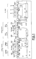
- FIG. 1 An hypothetical partial cross section of an integrated "smart power" type integrated device, wherein it is relatively easy to put in evidence, though in a schematic way, the aspects of the invention, is shown in Fig. 1.
- the depicted cross section does not include VDMOS power transistors, which may be easily imagined present in a different zone of the integrated device from the zone shown in the partial cross section of the figure, wherein two different CMOS structures are depicted, a first structure formed by an n-channel and a p-channel LDMOS transistor and a second structure formed by a p-channel and by an n-channel MOS transistor, and the structure of an isolated collector, vertical PNP bipolar transistor.
- the device comprises a p-type silicon substrate 1 on which an epitaxial n-type silicon layer 2 has been grown after doping with arsenic and/or with boron certain areas defined on the surface of the monocrystalline silicon substrate 1 in order to form the n + buried layers 3 and the p-type bottom isolations 4.
- the integrated device further comprises an isolation structure among the different integrated devices which, in the depicted example, is formed by a field oxide layer 5 grown on the surface of the silicon 2, after doping with boron predifined areas on the silicon surface in order to form, in accordance with well known techniques, the p-well regions 6 (i.e. top isolations and p-well) as well as regions with a heavier boron doping charge 11, also known as p-field region, while growing the field oxide 5, according to a known technique.
- gate structures 12 commonly of doped polycrystalline silicon, are formed.
- the structure of the isolated collector PNP vertical transistor comprises the collector (C) and emitter (E) contact p + diffusions 9 and the base (B) n + contact diffusion 10.
- an n-type region 8 extends from the surface of the epitaxial layer respectively in the drain area of the n-channel LDMOS transistor extending between the gate electrode and the isolation field oxide, in the source area of the p-channel LDMOS transistor extending between the gate electrode and the isolation field oxide, in the drain area of the n-channel MOS transistor extending between the gate electrode and the adjacent isolation field oxide and in the emitter area of the isolated collector PNP bipolar transistor defined by the surrounding isolation field oxide, for a depth sufficient to contain at least, respectively, the n + drain junction of the n-channel LDMOS transistor, the p + source junctions and n + body contact regions of the p-channel LDMOS transistor, the n + drain junction of the n-channel MOS transistor and the n + emitter junction of the PNP transistor.
- n-type regions 8 are made evident in the schematic cross section depicted in Fig. 1 by means of a thick line.
- the distinct regions 8 may be easily formed simultaneously in the indicated zones without requiring critical process steps by simply implanting phosphorus under self-alignment conditions in the indicated areas and by diffusing the implanted phosphorus before proceeding to the formation of the heavily doped n + regions obtained by implanting arsenic and diffusing it and of the heavily doped p + regions obtained by implanting boron and diffusing it, which are contained within said auxiliary regions 8.
- the doping level of this additional n-region 8 may be comprised between 10 13 and 10 14 (phosphorus) atoms per cubic centimeter.
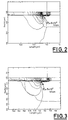
- Fig. 2 Shown in Fig. 2 are the equimodal electric field lines in the overlapping region between the drain and the gate of an n-channel LDMOS transistor having a 60 nm (600 Angstroms ( ⁇ )) thick gate oxide, produced by means of computer model simulation for the case of a transistor without the auxiliary n-doped region (8 of Fig. 1) in accordance with the present invention and subjected to a 20V bias.
- the maximum electric field intensity is evaluated to be 6 x 10 5 V/cm.
- the complementary LDMOS transistors depicted as forming a CMOS structure in Fig. 1, may themselves be employed as power transistors through an appropriate layout configuration, exploiting also for such applications, the same improved performance in terms of voltage withstanding ability and reduced resistance (R on ), derived by the presence of said additional n-region 8, in accordance with the present invention.
- the electrical performances of the other CMOS structure shown, formed by the pair of complementary MOS transistors, are improved because the n-region 8 formed in the drain region of the n-channel transistor acts as a drain extension region thus increasing the nominal operating voltage of the relative CMOS structure.
Description
- The present invention relates to a mixed technology, "smart power", integrated device containing power transistors and control logic and analog driving circuitry combined in a monolithic silicon chip.
- The commercial success of so-called "smart power" integrated circuits, wherein the analog signal processing circuitry, the control logic circuitry and the output power devices are conveniently monolithically integrated in a single chip, originated and sprung from the overcoming of compatibility problems among the different fabrication processes relative to the different integrated devices, often necessarily operating under different supply voltages. Most often, even though nonexclusively, the power section of such integrated circuits employs VDMOS transistors which typically require a driving gate voltage level comprised between about 10V - 20V.
- This makes difficult interfacing the power transistor (e.g. VDMOS) with the driving circuitry. Commonly, in fact, the maximum operating voltage of CMOS transistors used in logic circuitry is 5V. Conversely, the driving circuitry for power transistors operate at about 12V, while in order to ensure a driving level on the gate of a VDMOS power transistor of 10V and if a reasonable process "spread" is accounted for, the supply voltage of CMOS transistors of the relative driving circuit should be at least 15V. Moreover better operating conditions of a VDMOS power transistor (i.e. a lower resistance Ron) may be achieved if the driving voltage level on the gate may be raised to 15-20V, as it is well known to a skilled technician.
- In "smart power" type integrated circuits, this particular problem is commonly obviated by using a "level shifter" circuit, which necessarily makes the driving circuit more complicated.
- GB-A-2 186 117 discloses a semiconductor device comprising bipolar transistors, CMOS and vertical DMOS transistors.
- There is a definite need for the availability of CMOS transistors having an operating voltage of about 20V in a monolithically integrated semiconductor device of the "smart power" type in order to drive directly the output power transistors with a relatively high voltage without employing special level shifter circuits.
- On the other hand, in these integrated circuits there are other CMOS and bipolar transistors which are employed, because of their peculiar characteristics, in control logic circuitry and in signal processing circuitry, respectively. Also the utility and reliability of these other integrated devices could be advantageously enhanced if also these other integrated devices could be made capable of withstanding a higher supply voltage than the voltage normally allowed by the physical structure of these integrated devices produced through a mixed-technology fabrication process.
- In view of this state of the art, the present invention has the main objective of providing, in a monolithically integrated "smart power" type device, CMOS structures and isolated collector, vertical, PNP transistors capable of withstanding a higher operating voltage than the voltage normally withstood by these devices, when they are formed monolithically together in a single chip.
- This objective is reached by the integrated device of the invention, as defined in the annexed claims.
- Structurally the device is characterized by the fact that it comprises regions of phosphorus doped, n-type silicon of similar diffusion profile extending from the surface of the n-type epitaxial layer wherein the different devices are formed, respectively, through the drain area of n-channel LDMOS transistors extending between the gate electrode thereof and the adjacent isolating field oxide, the body area of p-channel LDMOS transistors, extending between the gate electrode thereof and the adjacent isolation field oxide, the drain area of n-channel MOS transistors, extending between the gate electrode thereof and the adjacent isolation field oxide, and the emitter area of isolated collector vertical PNP bipolar transistors, and by a depth sufficient to contain, respectively, the n+ doped drain region of n-channel LDMOS transistors, the p+ doped source region of p-channel LDMOS transistors, the n+ doped drain region of n-channel MOS transistors and the p+ doped emitter region of the PNP transistors.
- In the case of an n-channel LDMOS transistor, the presence of this auxiliary n-doped region, obtained by implanting phosphorus through the drain area, increases the breakdown voltage because the field intensity between the drain and the gate is reduced while obtaining a reduction too of the conducting resistance (Ron) of the transistor, which is extremely advantageous when the LDMOS transistor itself is used as an integrated power switching device, as it is often the case in these mixed technology integrated devices.
- In the case of a p-channel LDMOS transistor, the same auxiliary n- doped region may conveniently constitute a body region which is so formed without other specific additional process steps.
- The CMOS structures formed by pairs of complementary LDMOS transistors, when provided with such an n-doped region by phosphorus implantation, become capable of operating with a supply voltage of about 20V without requiring special precautions, such as "field plates", thus remaining advantageously compact.
- In the case of an n-channel MOS transistor belonging to another type of CMOS structure, the n-doped region, obtained by phosphorus implantation in the drain area of the transistor, reduces the sensitivity to electrical stresses due to hot electrons, by acting as a "drain extension" region; this permits to the transistor to withstand a supply voltage of about 12V.
- In the case of an isolated collector, vertical PNP bipolar transistor, the additional n-doped region obtained by phosphorus implantation through the emitter area of the transistor, permits to improve the transistor's performance transistors by increasing the charge in the base region of the transistor and to increase the "punchthrough" voltage between emitter and collector.
- The parallel ability of the different CMOS structures and vertical PNP transistors to withstand a specifically increased operating voltage specifically increased permits to build mixed technology integrated circuits (i.e. "smart power" devices) with far less pronounced interfacing problems among the different types of circuits, with enhanced possibilities of fully exploiting the intrinsic peculiarities of the different devices and with a higher degree of reliability.
- The peculiar aspects and advantages of the present invention, will become evident through the following detailed description of a preferred embodiment illustrated as a non-limitative example in the attached drawings, wherein:
- Fig. 1 is a partial schematic, sectional view of an integrated circuit made in accordance with the present invention;
- Fig. 2 shows equimodal, electric field lines in the overlapping region between the gate and the drain region of an n-channel LDMOS transistor of the prior art, without the additional n-doped region of the invention, produced by computer simulation;
- Fig. 3 shows equimodal electric field lines in the same overlapping region of the preceding figure, in the case of a transistor provided with the additional n-doped region in accordance with the present invention, produced by computer simulation.
- An hypothetical partial cross section of an integrated "smart power" type integrated device, wherein it is relatively easy to put in evidence, though in a schematic way, the aspects of the invention, is shown in Fig. 1. The depicted cross section does not include VDMOS power transistors, which may be easily imagined present in a different zone of the integrated device from the zone shown in the partial cross section of the figure, wherein two different CMOS structures are depicted, a first structure formed by an n-channel and a p-channel LDMOS transistor and a second structure formed by a p-channel and by an n-channel MOS transistor, and the structure of an isolated collector, vertical PNP bipolar transistor.
- The device comprises a p-
type silicon substrate 1 on which an epitaxial n-type silicon layer 2 has been grown after doping with arsenic and/or with boron certain areas defined on the surface of themonocrystalline silicon substrate 1 in order to form the n+ buriedlayers 3 and the p-type bottom isolations 4. The integrated device further comprises an isolation structure among the different integrated devices which, in the depicted example, is formed by afield oxide layer 5 grown on the surface of thesilicon 2, after doping with boron predifined areas on the silicon surface in order to form, in accordance with well known techniques, the p-well regions 6 (i.e. top isolations and p-well) as well as regions with a heavierboron doping charge 11, also known as p-field region, while growing thefield oxide 5, according to a known technique. - Within active areas destined to the formation of MOS-type devices,
gate structures 12, commonly of doped polycrystalline silicon, are formed. - Typically the n-channel, LDMOS transistor comprises a p-
body region 7, produced in the silicon by implanting boron under self-alignment conditions in the source area extending between thegate 12 and thefield oxide 5 and by successively diffusing the implanted boron until obtaining the desired diffusion profile of theregion 7, the n+ source anddrain junctions 10 and the p+ region 9 having a relatively high doping level formed in the source region for contacting thebody region 7. - Similarly a p-channel LDMOS transistor comprises a p-doped region 7 (having substantially the same profile of the n-channel LDMOS body region), formed in the drain region of the transistor, the p+ drain and
source junctions 9 and the n+ region 10, formed in the source area in order to contact an n-body region, the formation of which together with other n-regions in the different integrated structures according to the present invention will be described later. - The p-channel MOS transistor forming the second CMOS structure depicted in Fig. 1, comprises, as usual, the source and drain p+ junctions 9 and a "back gate" contact, n+ region 10, formed in the source zone of the transistor. Similarly the n-channel MOS transistor comprises the n+ source and
drain junctions 10 and a "back gate" contact, p+ region 9, formed in the source zone of the transistor. - The structure of the isolated collector PNP vertical transistor comprises the collector (C) and emitter (E) contact p+ diffusions 9 and the base (B) n+ contact diffusion 10.
- In accordance with the present invention, an n-
type region 8, doped with phosphorus, extends from the surface of the epitaxial layer respectively in the drain area of the n-channel LDMOS transistor extending between the gate electrode and the isolation field oxide, in the source area of the p-channel LDMOS transistor extending between the gate electrode and the isolation field oxide, in the drain area of the n-channel MOS transistor extending between the gate electrode and the adjacent isolation field oxide and in the emitter area of the isolated collector PNP bipolar transistor defined by the surrounding isolation field oxide, for a depth sufficient to contain at least, respectively, the n+ drain junction of the n-channel LDMOS transistor, the p+ source junctions and n+ body contact regions of the p-channel LDMOS transistor, the n+ drain junction of the n-channel MOS transistor and the n+ emitter junction of the PNP transistor. - These n-
type regions 8 are made evident in the schematic cross section depicted in Fig. 1 by means of a thick line. - As it will be evident to the skilled technician, the
distinct regions 8 may be easily formed simultaneously in the indicated zones without requiring critical process steps by simply implanting phosphorus under self-alignment conditions in the indicated areas and by diffusing the implanted phosphorus before proceeding to the formation of the heavily doped n+ regions obtained by implanting arsenic and diffusing it and of the heavily doped p+ regions obtained by implanting boron and diffusing it, which are contained within saidauxiliary regions 8. In a normal fabrication process the doping level of this additional n-region 8 may be comprised between 1013 and 1014 (phosphorus) atoms per cubic centimeter. - Shown in Fig. 2 are the equimodal electric field lines in the overlapping region between the drain and the gate of an n-channel LDMOS transistor having a 60 nm (600 Angstroms (Å)) thick gate oxide, produced by means of computer model simulation for the case of a transistor without the auxiliary n-doped region (8 of Fig. 1) in accordance with the present invention and subjected to a 20V bias. The maximum electric field intensity is evaluated to be 6 x 10⁵ V/cm.
- Similarly, shown in Fig. 3 are the equimodal electric field lines in the same overlapping region under identical bias conditions (20V) of the example shown in Fig. 2, but wherein the n-channel LDMOS transistor is provided with the auxiliary n-region, doped with phosphorus at 1014 atoms per cubic centimeter, in accordance with the present invention. As it is easily noted by comparing the Figures 2 and 3, in the latter the equimodal electric field lines are more "distended" than those of Fig. 1 and the maximum field electric intensity may be evaluated to be 5 x 10⁵ V/cm. This is 17% less than the maximum intensity evaluated in the case of the transistor of the prior art without the auxialiary phosphorus doped region.
- The CMOS structure formed by the complementary LDMOS transistors provided with the n-doped region 8 (Fig. 1) in accordance with the present invention may funtions with a supply voltage of 20 V and it may be directly interfaced, as a driving device, with VDMOS power transistors for example, thus eliminating the need for adequate level shifting circuits. Moreover, an LDMOS transistor structure modified according to the invention is intrinsically capable of withstanding voltages in the order of 20V without requiring the formation of "field plates" (according to a known technique for increasing the intrinsic breakdown voltage of integrated transistors) which inevitably clashes with compactness requirements of these integrated structures.
- Naturally, as it will appear evident to the skilled technician, the complementary LDMOS transistors, depicted as forming a CMOS structure in Fig. 1, may themselves be employed as power transistors through an appropriate layout configuration, exploiting also for such applications, the same improved performance in terms of voltage withstanding ability and reduced resistance (Ron), derived by the presence of said additional n-
region 8, in accordance with the present invention. - Also the electrical performances of the other CMOS structure shown, formed by the pair of complementary MOS transistors, are improved because the n-
region 8 formed in the drain region of the n-channel transistor acts as a drain extension region thus increasing the nominal operating voltage of the relative CMOS structure. - Another, non-negligeable advantage is obtained also in terms of improved performance of the isolated collector, vertical PNP bipolar transistor by providing also this integrated device with the n-
region 8 doped with phosphorus enchroaching in the base region of the transistor. The consequent increase of the doping level of the base region reduces sensitivity to depletion of the base region thus increasing the punchthrough voltage between emitter and collector. This permits also to this integrated component of the "smart power" device to function under a relatively high voltage, thus broadening the possibility of employing this type of transistor which is outstandingly suited, in respect to other types of transistors, for implementing circuits with a higher cut-off frequency then that which may be obtained by means of lateral PNP transistors.
Claims (3)
- A monolithically integrated circuit formed in an n-type epitaxial silicon layer (2) grown on a p-type monocrystalline silicon substrate (1) and comprising at least a first CMOS structure formed by a pair of complementary LDMOS transistors, the first having an n-type channel and the other a p-type channel, a second CMOS structure formed by a pair of complementary MOS transistors, a first having a p-type channel and the other an n-type channel, and at least an isolated collector, vertical PNP bipolar transistor,comprising first, second, third and fourthphosphorus doped n-type silicon regions (8) having the same diffusion profile which extend from the surface of said epitaxial layer, respectively in:a drain area of said n-channel LDMOS transistor defined between a gate electrode (12) of the transistor and an adjacent isolation field oxide (5),a source area of said p-channel LDMOS transistor defined between a gate electrode (12) of the transistor and an adjacent isolation field oxide (5),a drain area of said n-channel LDMOS transistor, defined between a gate electrode (12) of the transistor and an adjacent isolation field oxide (5), andan emitter area of said isolated collector, vertical PNP transistor, defined by a surrounding isolation field oxide (5),thereby extending into said epitaxial layer by a depth such that said regions contain, respectively:an n+ drain diffusion (10) of said n-channel LDMOS transistor,a p+ source diffusion (9) of said p-channel LDMOS transistor,an n+ drain diffusion (10) of said n-channel MOS transistor, anda p+ emitter diffusion (9) and further extending beyond said p+ emitter diffusion into a base region of said isolated collector, vertical PNP transistor.
- A monolithically integrated circuit as defined in claim 1, wherein said first CMOS structure is able to withstand a supply voltage of up to 20V and said second CMOS structure is able to withstand a supply voltage of up to 12V.
- A monolithically integrated circuit as defined in claim 2 wherein said first CMOS structure has no field-plates.
Applications Claiming Priority (2)
| Application Number | Priority Date | Filing Date | Title |
|---|---|---|---|
| IT8362689 | 1989-06-14 | ||
| IT8983626A IT1235843B (en) | 1989-06-14 | 1989-06-14 | INTEGRATED DEVICE CONTAINING POWER STRUCTURES FORMED WITH COMPLEMENTARY LDMOS TRANSISTORS, CMOS AND PNP VERTICAL STRUCTURES WITH INCREASED CAPACITY TO SUPPORT A HIGH SUPPLY VOLTAGE. |
Publications (3)
| Publication Number | Publication Date |
|---|---|
| EP0403449A2 EP0403449A2 (en) | 1990-12-19 |
| EP0403449A3 EP0403449A3 (en) | 1992-07-08 |
| EP0403449B1 true EP0403449B1 (en) | 1996-09-04 |
Family
ID=11323341
Family Applications (1)
| Application Number | Title | Priority Date | Filing Date |
|---|---|---|---|
| EP90830268A Expired - Lifetime EP0403449B1 (en) | 1989-06-14 | 1990-06-14 | Mixed technology intergrated device comprising complementary LDMOS power transistors, CMOS and vertical PNP integrated structures having an enhanced ability to withstand a relatively high supply voltage |
Country Status (5)
| Country | Link |
|---|---|
| US (1) | US5041895A (en) |
| EP (1) | EP0403449B1 (en) |
| JP (1) | JP3043367B2 (en) |
| DE (1) | DE69028354T2 (en) |
| IT (1) | IT1235843B (en) |
Families Citing this family (43)
| Publication number | Priority date | Publication date | Assignee | Title |
|---|---|---|---|---|
| US5465189A (en) * | 1990-03-05 | 1995-11-07 | Texas Instruments Incorporated | Low voltage triggering semiconductor controlled rectifiers |
| KR940009357B1 (en) * | 1991-04-09 | 1994-10-07 | 삼성전자주식회사 | Semiconductor device and manufacturing method thereof |
| US5204541A (en) * | 1991-06-28 | 1993-04-20 | Texas Instruments Incorporated | Gated thyristor and process for its simultaneous fabrication with high- and low-voltage semiconductor devices |
| US5157281A (en) * | 1991-07-12 | 1992-10-20 | Texas Instruments Incorporated | Level-shifter circuit for integrated circuits |
| JP3218642B2 (en) * | 1991-09-27 | 2001-10-15 | 富士電機株式会社 | Wiring structure of large current integrated circuit |
| US5225702A (en) * | 1991-12-05 | 1993-07-06 | Texas Instruments Incorporated | Silicon controlled rectifier structure for electrostatic discharge protection |
| US5446300A (en) * | 1992-11-04 | 1995-08-29 | North American Philips Corporation | Semiconductor device configuration with multiple HV-LDMOS transistors and a floating well circuit |
| EP0657995B1 (en) | 1993-12-07 | 1999-10-13 | STMicroelectronics S.r.l. | Mixed typology output stage |
| EP0658938B1 (en) * | 1993-12-15 | 2001-08-08 | STMicroelectronics S.r.l. | An integrated circuit comprising an EEPROM cell and a MOS transistor |
| US5498554A (en) * | 1994-04-08 | 1996-03-12 | Texas Instruments Incorporated | Method of making extended drain resurf lateral DMOS devices |
| JP3335060B2 (en) * | 1995-02-21 | 2002-10-15 | シャープ株式会社 | Method for manufacturing semiconductor device |
| JP3400181B2 (en) * | 1995-04-25 | 2003-04-28 | ローム株式会社 | Semiconductor device and manufacturing method thereof |
| US6831331B2 (en) | 1995-11-15 | 2004-12-14 | Denso Corporation | Power MOS transistor for absorbing surge current |
| US6242787B1 (en) | 1995-11-15 | 2001-06-05 | Denso Corporation | Semiconductor device and manufacturing method thereof |
| DE19548060A1 (en) * | 1995-12-21 | 1997-06-26 | Siemens Ag | Power semiconductor device with temperature sensor that can be controlled by field effect |
| EP0802567B1 (en) * | 1996-04-15 | 2007-08-29 | Denso Corporation | Semiconductor device having a power transistor structure |
| DE69618343D1 (en) * | 1996-05-21 | 2002-02-07 | Cons Ric Microelettronica | Power semiconductor device structure with vertical PNP transistor |
| US5950091A (en) * | 1996-12-06 | 1999-09-07 | Advanced Micro Devices, Inc. | Method of making a polysilicon gate conductor of an integrated circuit formed as a sidewall spacer on a sacrificial material |
| US6124174A (en) * | 1997-05-16 | 2000-09-26 | Advanced Micro Devices, Inc. | Spacer structure as transistor gate |
| US5866934A (en) * | 1997-06-20 | 1999-02-02 | Advanced Micro Devices, Inc. | Parallel and series-coupled transistors having gate conductors formed on sidewall surfaces of a sacrificial structure |
| TW421874B (en) * | 1998-01-09 | 2001-02-11 | Winbond Electronics Corp | Integrated structure for output buffer and silicon controlled rectifier |
| US6897525B1 (en) * | 1998-11-26 | 2005-05-24 | Sanyo Electric Co., Ltd. | Semiconductor device and method of manufacturing the same |
| JP3317345B2 (en) * | 1999-07-23 | 2002-08-26 | 日本電気株式会社 | Semiconductor device |
| US6818494B1 (en) * | 2001-03-26 | 2004-11-16 | Hewlett-Packard Development Company, L.P. | LDMOS and CMOS integrated circuit and method of making |
| JP4689861B2 (en) * | 2001-04-03 | 2011-05-25 | レンゴー株式会社 | carton |
| JP2003017577A (en) * | 2001-07-04 | 2003-01-17 | Denso Corp | Semiconductor device |
| US6768183B2 (en) * | 2001-04-20 | 2004-07-27 | Denso Corporation | Semiconductor device having bipolar transistors |
| JP4003438B2 (en) * | 2001-11-07 | 2007-11-07 | 株式会社デンソー | Semiconductor device manufacturing method and semiconductor device |
| JP3970689B2 (en) * | 2002-05-30 | 2007-09-05 | エルピーダメモリ株式会社 | Semiconductor device and manufacturing method thereof |
| US7825488B2 (en) | 2006-05-31 | 2010-11-02 | Advanced Analogic Technologies, Inc. | Isolation structures for integrated circuits and modular methods of forming the same |
| US6855985B2 (en) | 2002-09-29 | 2005-02-15 | Advanced Analogic Technologies, Inc. | Modular bipolar-CMOS-DMOS analog integrated circuit & power transistor technology |
| US7019377B2 (en) * | 2002-12-17 | 2006-03-28 | Micrel, Inc. | Integrated circuit including high voltage devices and low voltage devices |
| SE0303106D0 (en) * | 2003-11-21 | 2003-11-21 | Infineon Technologies Ag | Ldmos transistor device, integrated circuit, and fabrication method thereof |
| US7230302B2 (en) * | 2004-01-29 | 2007-06-12 | Enpirion, Inc. | Laterally diffused metal oxide semiconductor device and method of forming the same |
| JP4795869B2 (en) * | 2006-06-26 | 2011-10-19 | レンゴー株式会社 | Package |
| US7781843B1 (en) | 2007-01-11 | 2010-08-24 | Hewlett-Packard Development Company, L.P. | Integrating high-voltage CMOS devices with low-voltage CMOS |
| US20090127629A1 (en) * | 2007-11-15 | 2009-05-21 | Zia Alan Shafi | Method of forming npn and pnp bipolar transistors in a CMOS process flow that allows the collectors of the bipolar transistors to be biased differently than the substrate material |
| US7906810B2 (en) * | 2008-08-06 | 2011-03-15 | United Microelectronics Corp. | LDMOS device for ESD protection circuit |
| KR101681494B1 (en) * | 2010-03-03 | 2016-12-01 | 삼성전자 주식회사 | Semiconductor device |
| CN102176467B (en) * | 2011-03-29 | 2016-03-23 | 上海华虹宏力半导体制造有限公司 | Slot type MOSFET |
| US9214457B2 (en) | 2011-09-20 | 2015-12-15 | Alpha & Omega Semiconductor Incorporated | Method of integrating high voltage devices |
| US9356512B2 (en) * | 2013-07-29 | 2016-05-31 | Broadcom Corporation | Envelope tracking power supply with direct connection to power source |
| GB2561388B (en) * | 2017-04-13 | 2019-11-06 | Raytheon Systems Ltd | Silicon carbide integrated circuit |
Family Cites Families (9)
| Publication number | Priority date | Publication date | Assignee | Title |
|---|---|---|---|---|
| US4120707A (en) * | 1977-03-30 | 1978-10-17 | Harris Corporation | Process of fabricating junction isolated IGFET and bipolar transistor integrated circuit by diffusion |
| FR2571178B1 (en) * | 1984-09-28 | 1986-11-21 | Thomson Csf | INTEGRATED CIRCUIT STRUCTURE HAVING HIGH VOLTAGE HOLD CMOS TRANSISTORS, AND MANUFACTURING METHOD THEREOF |
| JPS61166071A (en) * | 1985-01-17 | 1986-07-26 | Toshiba Corp | Semiconductor device and manufacture thereof |
| JPS61281544A (en) * | 1985-06-06 | 1986-12-11 | Fuji Electric Co Ltd | Manufacture of semiconductor integrated circuit |
| JPS62119936A (en) * | 1985-11-19 | 1987-06-01 | Fujitsu Ltd | Complementary lsi chip |
| GB2186117B (en) * | 1986-01-30 | 1989-11-01 | Sgs Microelettronica Spa | Monolithically integrated semiconductor device containing bipolar junction,cmosand dmos transistors and low leakage diodes and a method for its fabrication |
| JPH01140759A (en) * | 1987-11-27 | 1989-06-01 | Nec Corp | Bi-mos semiconductor device |
| JPH01272145A (en) * | 1988-04-25 | 1989-10-31 | Hitachi Ltd | Semiconductor integrated circuit device and manufacture thereof |
| US4918026A (en) * | 1989-03-17 | 1990-04-17 | Delco Electronics Corporation | Process for forming vertical bipolar transistors and high voltage CMOS in a single integrated circuit chip |
-
1989
- 1989-06-14 IT IT8983626A patent/IT1235843B/en active
-
1990
- 1990-06-08 US US07/535,774 patent/US5041895A/en not_active Ceased
- 1990-06-14 JP JP2156586A patent/JP3043367B2/en not_active Expired - Fee Related
- 1990-06-14 EP EP90830268A patent/EP0403449B1/en not_active Expired - Lifetime
- 1990-06-14 DE DE69028354T patent/DE69028354T2/en not_active Expired - Fee Related
Also Published As
| Publication number | Publication date |
|---|---|
| EP0403449A3 (en) | 1992-07-08 |
| US5041895A (en) | 1991-08-20 |
| EP0403449A2 (en) | 1990-12-19 |
| JPH0324758A (en) | 1991-02-01 |
| IT8983626A0 (en) | 1989-06-14 |
| DE69028354T2 (en) | 1997-01-23 |
| JP3043367B2 (en) | 2000-05-22 |
| DE69028354D1 (en) | 1996-10-10 |
| IT1235843B (en) | 1992-11-03 |
Similar Documents
| Publication | Publication Date | Title |
|---|---|---|
| EP0403449B1 (en) | Mixed technology intergrated device comprising complementary LDMOS power transistors, CMOS and vertical PNP integrated structures having an enhanced ability to withstand a relatively high supply voltage | |
| US4862233A (en) | Integrated circuit device having vertical MOS provided with Zener diode | |
| US5286995A (en) | Isolated resurf LDMOS devices for multiple outputs on one die | |
| US7265434B2 (en) | Modular bipolar-CMOS-DMOS analog integrated circuit and power transistor technology | |
| US6420771B2 (en) | Trench isolated bipolar transistor structure integrated with CMOS technology | |
| US5066602A (en) | Method of making semiconductor ic including polar transistors | |
| EP0658938B1 (en) | An integrated circuit comprising an EEPROM cell and a MOS transistor | |
| US5602416A (en) | Power integrated circuit ("PIC") structure | |
| US5874768A (en) | Semiconductor device having a high breakdown voltage | |
| US5218228A (en) | High voltage MOS transistors with reduced parasitic current gain | |
| US5132235A (en) | Method for fabricating a high voltage MOS transistor | |
| US5990535A (en) | Power integrated circuit | |
| US5912495A (en) | High voltage driver circuit with diode | |
| US5703385A (en) | Power integrated circuit ("PIC") structure with a vertical IGBT | |
| USRE37424E1 (en) | Mixed technology integrated device comprising complementary LDMOS power transistors, CMOS and vertical PNP integrated structures having an enhanced ability to withstand a relatively high supply voltage | |
| US6472710B2 (en) | Field MOS transistor and semiconductor integrated circuit including the same | |
| US5317182A (en) | Termination of the power stage of a monolithic semiconductor device | |
| KR0169965B1 (en) | A monolithic integrated circuit including assitant ldmos power transistor, cmos and vertical pnp integrated structures | |
| US6030888A (en) | Method of fabricating high-voltage junction-isolated semiconductor devices | |
| JPH0529615A (en) | Semiconductor device having conductivity modulated misfet |
Legal Events
| Date | Code | Title | Description |
|---|---|---|---|
| PUAI | Public reference made under article 153(3) epc to a published international application that has entered the european phase |
Free format text: ORIGINAL CODE: 0009012 |
|
| AK | Designated contracting states |
Kind code of ref document: A2 Designated state(s): DE FR GB NL SE |
|
| PUAL | Search report despatched |
Free format text: ORIGINAL CODE: 0009013 |
|
| AK | Designated contracting states |
Kind code of ref document: A3 Designated state(s): DE FR GB NL SE |
|
| 17P | Request for examination filed |
Effective date: 19921217 |
|
| 17Q | First examination report despatched |
Effective date: 19940913 |
|
| GRAH | Despatch of communication of intention to grant a patent |
Free format text: ORIGINAL CODE: EPIDOS IGRA |
|
| GRAH | Despatch of communication of intention to grant a patent |
Free format text: ORIGINAL CODE: EPIDOS IGRA |
|
| GRAA | (expected) grant |
Free format text: ORIGINAL CODE: 0009210 |
|
| AK | Designated contracting states |
Kind code of ref document: B1 Designated state(s): DE FR GB NL SE |
|
| REF | Corresponds to: |
Ref document number: 69028354 Country of ref document: DE Date of ref document: 19961010 |
|
| ET | Fr: translation filed | ||
| PLBE | No opposition filed within time limit |
Free format text: ORIGINAL CODE: 0009261 |
|
| STAA | Information on the status of an ep patent application or granted ep patent |
Free format text: STATUS: NO OPPOSITION FILED WITHIN TIME LIMIT |
|
| 26N | No opposition filed | ||
| REG | Reference to a national code |
Ref country code: FR Ref legal event code: D6 |
|
| PGFP | Annual fee paid to national office [announced via postgrant information from national office to epo] |
Ref country code: SE Payment date: 20010417 Year of fee payment: 12 |
|
| REG | Reference to a national code |
Ref country code: GB Ref legal event code: IF02 |
|
| PGFP | Annual fee paid to national office [announced via postgrant information from national office to epo] |
Ref country code: FR Payment date: 20020610 Year of fee payment: 13 |
|
| PGFP | Annual fee paid to national office [announced via postgrant information from national office to epo] |
Ref country code: GB Payment date: 20020612 Year of fee payment: 13 |
|
| PG25 | Lapsed in a contracting state [announced via postgrant information from national office to epo] |
Ref country code: SE Free format text: LAPSE BECAUSE OF NON-PAYMENT OF DUE FEES Effective date: 20020615 |
|
| PGFP | Annual fee paid to national office [announced via postgrant information from national office to epo] |
Ref country code: DE Payment date: 20020619 Year of fee payment: 13 |
|
| EUG | Se: european patent has lapsed | ||
| PG25 | Lapsed in a contracting state [announced via postgrant information from national office to epo] |
Ref country code: GB Free format text: LAPSE BECAUSE OF NON-PAYMENT OF DUE FEES Effective date: 20030614 |
|
| PG25 | Lapsed in a contracting state [announced via postgrant information from national office to epo] |
Ref country code: DE Free format text: LAPSE BECAUSE OF NON-PAYMENT OF DUE FEES Effective date: 20040101 |
|
| GBPC | Gb: european patent ceased through non-payment of renewal fee |
Effective date: 20030614 |
|
| PG25 | Lapsed in a contracting state [announced via postgrant information from national office to epo] |
Ref country code: FR Free format text: LAPSE BECAUSE OF NON-PAYMENT OF DUE FEES Effective date: 20040227 |
|
| REG | Reference to a national code |
Ref country code: FR Ref legal event code: ST |
|
| PGFP | Annual fee paid to national office [announced via postgrant information from national office to epo] |
Ref country code: NL Payment date: 20040603 Year of fee payment: 15 |
|
| PG25 | Lapsed in a contracting state [announced via postgrant information from national office to epo] |
Ref country code: NL Free format text: LAPSE BECAUSE OF NON-PAYMENT OF DUE FEES Effective date: 20060101 |
|
| NLV4 | Nl: lapsed or anulled due to non-payment of the annual fee |
Effective date: 20060101 |