EP0403396B1 - Einrichtung zur Überwachung des Betriebs eines Mikrokontrollers oder Mikroprozessors - Google Patents
Einrichtung zur Überwachung des Betriebs eines Mikrokontrollers oder Mikroprozessors Download PDFInfo
- Publication number
- EP0403396B1 EP0403396B1 EP19900401689 EP90401689A EP0403396B1 EP 0403396 B1 EP0403396 B1 EP 0403396B1 EP 19900401689 EP19900401689 EP 19900401689 EP 90401689 A EP90401689 A EP 90401689A EP 0403396 B1 EP0403396 B1 EP 0403396B1
- Authority
- EP
- European Patent Office
- Prior art keywords
- signal
- input
- flag
- output
- flip
- Prior art date
- Legal status (The legal status is an assumption and is not a legal conclusion. Google has not performed a legal analysis and makes no representation as to the accuracy of the status listed.)
- Expired - Lifetime
Links
Images


Classifications
-
- G—PHYSICS
- G06—COMPUTING OR CALCULATING; COUNTING
- G06F—ELECTRIC DIGITAL DATA PROCESSING
- G06F11/00—Error detection; Error correction; Monitoring
- G06F11/07—Responding to the occurrence of a fault, e.g. fault tolerance
- G06F11/0703—Error or fault processing not based on redundancy, i.e. by taking additional measures to deal with the error or fault not making use of redundancy in operation, in hardware, or in data representation
- G06F11/0751—Error or fault detection not based on redundancy
- G06F11/0754—Error or fault detection not based on redundancy by exceeding limits
- G06F11/0757—Error or fault detection not based on redundancy by exceeding limits by exceeding a time limit, i.e. time-out, e.g. watchdogs
-
- G—PHYSICS
- G06—COMPUTING OR CALCULATING; COUNTING
- G06F—ELECTRIC DIGITAL DATA PROCESSING
- G06F1/00—Details not covered by groups G06F3/00 - G06F13/00 and G06F21/00
- G06F1/24—Resetting means
Definitions
- the present invention relates to a device for monitoring the operation of a microcontroller or microprocessor, in particular but not exclusively for application to motor vehicles.
- microcontrollers and microprocessors generally deliver on one of their outputs, a control signal whose frequency depends on the operation of the microcontroller or microprocessor, that is to say the progress of programming.
- Such monitoring is particularly useful when microcontrollers or microprocessors are used in environments highly disturbed by electromagnetic interference, as is the case in particular in motor vehicles.
- the circuits proposed for this purpose are generally formed by two monostables which have corresponding switching times respectively to the minimum period and to the maximum period admissible in normal operation of the control signal generated by the microprocessor.
- Document US-A-4347608 describes a self-control system for electronic processor equipment.
- the control system includes a ROM memory storing a plurality of firmware in individual areas addressable by the processor.
- a timing circuit is activated to determine the frequency of pulses controlling a counter which calls successive phases of the selected firmware. Code words read during these phases and coming from a logic network associated with the processor are applied to the latter for a comparison with the corresponding contents of the program memory.
- an alarm indicator is activated.
- control unit comprises an oscillator which delivers a timing signal of constant and known frequency, a programmable frequency divider which receives the timing signal as an input and delivers a signal at its output clock, and the aforementioned counter receiving the clock signal.
- the present invention now aims to provide a new monitoring device which eliminates the drawbacks of prior devices.
- An auxiliary object of the present invention is to provide a circuit that can be integrated into a single housing.
- Another auxiliary object of the present invention is to provide a more precise device than the devices prior to two monostable devices.
- Another auxiliary object of the present invention is to provide a monitoring device allowing easy and fairly wide adjustment of the authorized frequency range.
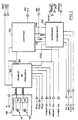
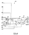
- FIG. 1 appended Found in FIG. 1 appended are the four main functional blocks of the monitoring device according to the present invention, previously indicated: an oscillator 100, a frequency divider 200, a counter 300 and an event controller 400.
- the function of the oscillator 100 is to deliver a timing signal of constant and known frequency.
- the frequency divider 200 is programmable. It receives as input the timing signal generated by the oscillator 100 and delivers at its output 201 a clock signal HC whose period is linked to the minimum period authorized for the control signal from the microcontroller or the microprocessor.
- the counter 300 receives the clock signal HC and generates time windows therefrom. These time windows are identified by the validation of flags on the outputs TM, DBF1 and FINF of the counter, that is to say a passage to the high level of these outputs.
- the event controller 400 receives the control signal from the microcontroller or microprocessor and monitors the state of this control signal during the time windows generated by the counter 300.
- the control signal generated by the microcontroller or microprocessor is referenced SM in the attached figures.
- the event controller 400 In the event of an anomaly noted, that is to say when the period of the control signal SM leaves a defined range, the event controller 400 generates a reset signal from the microcontroller or microprocessor on its RESET output. .
- the oscillator module 100 in fact comprises two oscillators 110, 120, associated with respective crystals 112, 122, and connected respectively to the input terminals OSLOW and OSQUIC of the frequency divider 200.
- These oscillators 110, 120 can work for example in the frequency range from 2 to 20 MHz for the oscillator 110 and in the range from 20 to 32 MHz for the oscillator 120. Only one of the two oscillators 110, 120 is set service to control the monitoring circuit. The choice of the oscillator to activate depends on the frequency of the control signal generated by the microcontroller or microprocessor to be monitored.
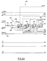
- FIGS. 2A and 2B The diagram of the frequency divider 200 is shown in FIGS. 2A and 2B which are complementary.
- the frequency divider 200 comprises on the one hand a set 210 of flip-flops connected in cascade to divide the frequency of the timing signal OSLOW or OSQUIC coming from the oscillator 100, on the other hand a multiplexer 250 which generates the clock signal HC from signals generated by the flip-flop set 210, as a function of an external three-bit programming word applied to inputs V1, V2, V3 of the module.
- two sets of four flip-flops 211, 212, 213, 214 are provided on the one hand, and 215, 216, 217 and 218 on the other hand.
- the OSLOW and OSQUIC inputs of module 200 are connected to the inputs of a NOR gate 219.
- the output of gate 219 attacks, via an inverter 220, the clock inputs CLK of flip-flops 211 and 215.
- the CLR reset inputs of flip-flops 211 to 218 receive, via inverters 221, 222, 223, a reset signal when the system is powered up, applied from outside the circuit to an input RAZINIT.
- the output Q / of the flip-flop 211 is looped back to its input D and connected to the clock input CLK of the flip-flop 212 downstream. It is the same for the flip-flop 212 which has its output Q / looped back to its input D is connected to the clock input CLK of the flip-flop 213; the latter itself has its output Q / looped back to its input D and connected to the clock input CLK of the flip-flop 214.
- This flip-flop 214 has its output Q / looped back to its output D.
- the outputs Q of flip-flops 211, 212, 213 and 214 are connected to the respective inputs of a NAND gate 224. The output of this latter is connected to the input of a NAND gate 225. The second input of the NAND gate 225 receives a test signal applied from the outside to a TURBOH input.
- the output of the NAND gate 225 is connected to a first input of a door or exclusive 226.
- the second input of this door is connected to the output Q of the flip-flop 215.
- the output of the door or exclusive 226 attacks the input D of rocker 215.
- the Q / output of the flip-flop 215 is connected to the CLK clock input of the flip-flop 216.
- the Q / output of the flip-flop 216 is looped back to its D input and is connected to the CLK clock input of the flip-flop 217.
- the output Q / of the bacule 217 is looped back to its input D and connected to the clock input CLK of the flip-flop 218.
- the output Q / of flip-flop 218 is looped back to its input D.
- the frequency of the oscillator 110 or 120 used to drive the monitoring circuit is available on an HBUFF output of the module 200. In fact, this output is connected to the output of the NOR 219 door by means of two non- series 227, 228.
- the divider module 200 delivers on outputs HDIV and PHI1 a signal whose frequency corresponds to that of the oscillator 110 or 120 used, divided by 256.
- the signals HDIV and PHI1 are obtained on the basis of the outputs Q of the flip-flops 211, 218 and a TURPHI test signal.
- the TURPHI test input of the module 200 as well as the Q output of the flip-flop 211 are connected to the inputs of an ET229 gate.
- a second gate ET230 receives on its inputs the output Q of the flip-flop 218, and the signal TURPHI complemented by a gate NO 231.
- the outputs of the gates E229, 230 attack the inputs of a gate NOR 232.
- the output of the gate NOR 232 is connected to the HDIV and PHI1 outputs of module 200 respectively by NON gates 233, 234.
- the HDIV output can be used to drive a microcontroller.
- the PHI1 output is used to control the event controller 400.
- the purpose of the mutiplexer 250 is to generate the clock signal HC on the basis of the intermediate frequency signals generated by the set of flip-flops 210, and on the basis of the programming word defined on the inputs V1, V2, V3 .
- the multiplexer 250 is formed of NON gates 251, 252, 253, 254, 255, 256, NAND gates with two inputs 257, 258, 259, 260, NOR gates 261, 262, 263, 264, 265, 266, 267 and 268, AND doors with two inputs 269, 270, 271, 272, 273, 274, 275, 276, NOR doors 277, 278, 279, 280 and one NAND gate with four inputs 281.
- the gates 251 to 268 define a logical combination of the inputs V1, V2 and V3.
- the outputs of doors 261 to 268 are connected to one of the inputs of AND gates 269 to 276.
- the second input of these doors 269 to 276 receives one of the Q outputs of flip-flops 211 to 217 or the output of door 234
- the multiplexer 250 with logic gates in FIG. 2B can be the subject of various variant embodiments. For this reason, the particular structure of the multiplexer, that is to say the exact connections defined between the logic gates, will not be described in more detail below.
- the logic state imposed on the inputs V1, V2 and V3, which corresponds to the programming word of the division, makes it possible to indirectly define the minimum period threshold for the control signal from the microcontroller or microprocessor.
- the state of the inputs V1, V2 and V3 makes it possible to determine the frequency of the clock signal HC, and the minimum period threshold is defined by the counter 300 as being equal to a multiple of the period of the clock signal HC.
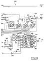
- the structure of the counter 300 is shown in Figures 3A, 3B, taken in combination.
- the essential function of the counter 300 is to generate, from the clock signal HC, time windows.
- the essential function of the counter 300 is to generate three flags: a first flag defining a so-called dead time period during which the state of the control signal generated by the microcontroller to the microprocessor is indifferent, and two flags corresponding respectively to the minimum period and the maximum period between which the period of the control signal must lie.
- the counter 300 is essentially formed by fifteen flip-flops 301 to 315 connected in cascade, clocked by the clock signal HC, and associated with flip-flops making it possible to store the flags of dead time and minimum period generated by flip-flops 301 at 315.
- the clock signal HC from the frequency divider 200 is applied to the clock inputs CLK of the flip-flop 301, of the flip-flop 304 and of the flip-flop 308, by means of an inverter 316.
- the CLR reset inputs of flip-flops 301 to 315 receive an internal reset reset signal generated by the event controller 400 according to methods which will be described later.
- the reset signal is applied to flip-flops 301 to 315 via inverters 317 to 321.
- the Q / output of flip-flop 301 is looped back to its D input and connected to the CLK clock input of the downstream flip-flop 302.
- the Q / output of flip-flop 302 is looped back to its D input and connected to the input CLK clock of flip-flop 303.
- the Q / output of flip-flop 303 is connected to its input D.
- the outputs Q of flip-flops 301, 302 and 303 are connected to the inputs of a NAND gate 322.
- the output of gate 322 is connected to a first input of a NAND gate 323, the second input of which receives, via an inverter 324, a TURBOC test signal applied from the outside.
- the output of door 323 is connected to a first input of a door or exclusive 325, the second input of which receives the output Q of the flip-flop 304.
- the output of the door or exclusive 325 is connected to the input D of the flip-flop 304.
- the output Q / of the flip-flop 304 is connected to the input d CLK clock of flip-flop 305.
- the Q / output of flip-flop 305 is looped back to its D input and connected to the CLK input of flip-flop 306.
- the Q / output of flip-flop 306 is looped back to its D input and connected at the CLK clock input of flip-flop 307.
- the Q / output of flip-flop 307 is looped back to its input D.
- the output of the NAND gate 322 and the Q output of the flip-flop 304 attack the inputs of a NOR gate 326.
- the inputs of a NAND gate 327 receive the output of this gate 326 as well as the Q outputs of the flip-flops 305 to 307.
- the same output of the NAND gate 328 is connected to one of the inputs of a gate or exclusive 329 which receives on its second input the output Q of the flip-flop 308.
- the output of the door or exclusive 329 is connected to the input D of the flip-flop 308.
- the output Q / of the flip-flop 308 is connected to the clock input CLK of the flip-flop 309.
- the output Q / of the flip-flop 309 is looped back to its D input and connected to the CLK clock input of flip-flop 310.
- the Q / output of flip-flop 310 is looped back to its D input and connected to the CLK clock input of flip-flop 311
- the Q / output of flip-flop 311 is looped back to its D input and connected to the CLK clock input of flip-flop 312.
- the Q / output of flip-flop 312 is looped back to its D input and connected to the input CLK clock of flip-flop 313.
- the Q / output of flip-flop 313 is looped back to its D input and connected to the CLK clock input of flip-flop 314.
- the Q / output of flip-flop 314 is looped back to its input D and connected to the CLK clock input of flip-flop 315.
- the Q / output of flip-flop 315 is looped back to its input D.
- the dead time, minimum period and maximum period flags are available respectively on outputs referenced TN, DBF1 and FINF of the counter 300.
- the dead time flag available on the output TM is defined using the output Q of the flip-flop 310 stored on a flip-flop SR formed by two NOR gates 330, 331. For this the output Q of the flip-flop 310 is applied to a first input of door 330. The output of door 330 is connected to a first input of door 331. The latter receives on its second input the reset internal reset signal via the inverter 317 The output of door 331 is connected to the output TM of counter 300. It is also looped back to the second input of door 330.
- the flag corresponding to the minimum period, available on the output DBF1 is defined on the basis of the output Q of the flip-flop 313, stored on a flip-flop SR formed by two NOR gates 332, 333.
- the output Q of flip-flop 313 is connected to a first input of door 332.
- the output of door 332 is connected to a first input of door 333. This receives on its second input the internal reset signal by l 'through the inverter 317.
- the output of the NOR gate 303 is connected to the output DBF1 of the counter 300. It is also connected to the second input of the gate 332.
- the duration of the dead time defined by the flag TM corresponds to 1/8 of the minimum period defined by the flag DBF1.
- the flag of maximum period, available on the FINF output of the counter 300 is defined as desired on the basis of the Q output of the flip-flop 314, or on the basis of the Q output of the flip-flop 315.
- the choice between these two possibilities is made by checking the state of a TL input of the circuit.
- the output Q of the flip-flop 314 is connected to a first input of an AND gate 334, which receives on its second input, via an inverter 335, the control signal TL.
- the output Q of the flip-flop 315 is in turn connected to the first input of an AND gate 336 which receives on its second input the signal TL.
- the outputs of doors 334, 336 are connected to the inputs of a NOR gate 337, the output of which is connected to the terminal FINF by means of an inverter 338.
- the maximum period controlled, defined by the FINF flag corresponds either to twice the minimum period defined by the DBF1 flag, or to four times this minimum period.
- flip-flops 301 to 315 are mounted as asynchronous counters, a re-synchronization on the basis of the clock signal HC being provided at the input of flip-flops 301, 304 and 308.
- the TURBOC test signal makes it possible to inhibit the part of the counter formed by the flip-flops 301 to 307, to operate in test mode at a faster frequency. However, in normal mode of monitoring the operation of the microcontroller or microprocessor, the TURBOC test signal is inhibited.
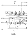
- the structure of the event controller 400 is shown in FIGS. 4A and 4B complementary.
- the main function of the event controller 400 is to control the state of the control signal generated by the microcontroller or microprocessor, during the time windows defined by the counter 300.
- the control signal generated by the microcontroller or microprocessor is applied to the SM input of the event controller 400.
- the purpose of the event controller 400 is to verify that the control signal SM passes indeed from the low level to the high level between the minimum period defined by the flag DBF1 and the maximum period defined by the flag FINF.
- the event controller ensures a reset of the counter 300, and therefore of the time windows, by validation of the reset signal.
- the state of the control signal SM generated by the microcontroller or microprocessor is ignored as long as the dead time flag TM is not validated, that is to say as long as this flag TM is at zero.
- control signal SM is applied to a first input of a NOR 401 gate, the output of which is connected to the first input of a NOR 402 gate.
- the output of the NOR 402 gate is looped back to the second input of door 401.
- the second input of door 402 receives the signal TM via an inverter 403.
- the signal coming from the gate 402, as well as the flags DBF1 and FINF are the object of a double memorization, in flip-flops 404 to 409, successively on the rising edge then on the falling edge of the signal PHI1 coming from the frequency divider 200.
- the output of the gate 402 is connected to the input D of the flip-flop 404.
- the output Q of this flip-flop 404 is connected to the input D of the flip-flop 405.
- the flag DBF1 of minimum period is applied to the input D of the flip-flop 406.
- the output Q of this flip-flop 406 is connected to input D of flip-flop 407.
- the maximum period flag defined on the FINF input is applied to the D input of the flip-flop 408.
- the Q output of this is applied to the D input of the flip-flop 409.
- the CLK clock inputs of the flip-flops 404, 406 and 408 receive the PHI1 signal via two inverters 410, 411.
- the CLK clock inputs of the output flip-flops 405, 407 and 409 receive the PHI1 signal complemented by three inverters 410, 412 and 413.
- the CLR reset inputs of the output flip-flops 405, 407 and 409 receive the reset signal on power-up RAZINIT, applied from the outside, via inverters 414, 415.
- the inputs of resetting the input flip-flops 404, 406 and 408 receive an internal reset signal, corresponding to the RESET signal, defined at the output of an inverter 416 according to methods which will be defined later.
- the event controller 400 includes a logic module formed by three NOR doors 417, 418, 419 and two NAND doors 420, 421 which combine the outputs of flip-flops 405, 407 and 409, to verify that the SM control signal available to the exit from gate 402 when the dead time flag TM is at the high logic level, itself passes from the low logic level to the high logic level between the validation of the two flags DBF1 and FINF.
- the NOR gate 417 receives on its inputs the outputs Q / of the gates 405 and 407.
- the NOR gate 418 receives on its inputs the output Q / of the flip-flop 405 and the output Q of flip-flop 407.
- NOR gate 419 receives on its inputs the output of gate 418 and the Q output of flip-flop 409.
- gate NOR 417 The output of gate NOR 417 is validated when the control signal SM passes from the low logic level to the high logic level after validation of the flag DBF1. This information is stored on a flip-flop 422 which receives on its input D the output of door 417. The output Q / of flip-flop 422 is used to generate the internal reset signal RESET, that is to say reset counter 300 and the corresponding time windows.
- the output of the NOR gate 419 is connected to a first input of a NAND gate 420 which receives on its second input a signal derived from the control signal MV, according to methods which will be explained later.
- the output of gate 420 is validated in the event of detection of abnormal operation, that is to say when the signal SM is at zero at the end of the dead time defined by the flag TM, or even when the signal SM goes to logic level high before validation of the flag DBF1, or again when the control signal SM does not pass to logic level high before the validation of the flag of maximum period FINF.
- the information available on the output of door 420 is stored in a flip-flop 423 whose input D is connected to the output of door 420.
- the Q / output of flip-flop 423 is used to generate the RESET signal for general reset from the microprocessor to the microcontroller.
- CLK clock inputs of flip-flops 422, 423 receive signal PHI1 via inverters 410, 411.
- CLR reset inputs of flip-flops 422, 423 receive signal RAZINIT of reset to power up via inverters 414 and 415.
- a NAND gate 425 receives respectively on its three inputs the output Q / of the flip-flop 422, the signal RAZINIT of general reset at power-up, by means of an inverter 424, and the output of a NAND gate 421. This receives on its inputs respectively the output of gate NOR 419 and the output of gate NAND 425.
- the output of this door 425 is connected to a DFLT output terminal of the device via an inverter 426.
- the DFLT output goes to 1 when the period of the control signal generated by the microcontroller to the microprocessor leaves the authorized window . In in other words, the DFLT output goes to 1 in the event of a malfunction of the microcontroller or microprocessor.
- a NAND gate with two inputs 428 receives on its inputs the output Q / of the flip-flop 423 and an external signal SDR.
- the output of gate 428 is connected via two inverters 429, 430 to the RESET output terminal of the monitoring device, on which the reset signal from the microcontroller or microprocessor is available.
- RESETB the terminal referenced RESETB
- a NAND gate 427 with four inputs receives a signal derived from the control signal MV, the output Q / of the flip-flop 422 and the output of the inverter 429 and the output of the inverter 424.
- the output of gate 427 is connected at the input of the inverter 416. It is also connected to the reset output via an inverter 402.
- the reset signal of the counter 300 in the event of detection of correct operation, is available on the reset terminal.
- the same signal, complemented, is available on the output referenced SYNCRAZ, which is connected to the output of the inverter 432 via an inverter 433.
- the DR and MV signals are processed by a set of ten flip-flops 434 to 443.
- the signal DR is applied to the input D of the flip-flop 434.
- the output Q of this flip-flop is connected to the input D to the flip-flop 439.
- the Q output of the flip-flop 439 is connected to the input D of the flip-flop 438.
- the output Q of the flip-flop 438 is connected to the input D of the flip-flop 443.
- the signal MV is applied to the input D of the flip-flop 435.
- the output Q of the flip-flop 435 is connected to the input D of the flip-flop 440.
- the Q output of the flip-flop 440 is connected to the input D of the flip-flop 436.
- the output Q of flip-flop 436 is connected to the input D of flip-flop 441.
- the output Q of flip-flop 441 is connected to input D of flip-flop 437.
- the output Q of the flip-flop 437 is connected to the input D of the flip-flop 442.
- the CLR reset inputs of flip-flops 434 to 443 receive the signal RAZINIT via inverters 444, 445.
- the CLK clock inputs of flip-flops 434 to 438 receive the signal PHI1 through inverters 410 , 446.
- the flip-flops 439 to 443 receive the signal PHI1 supplemented via three inverters 410, 412 and 447.
- the Q output of flip-flop 439 and the Q / output of flip-flops 442 and 443 are combined in a NAND gate 448 The output of the latter attacks the input of the NAND gate 420. Furthermore the output Q of the flip-flop 436 attacks one of the inputs of the NAND gate 427.
- the MV input enables validation or invalidation of the monitoring of the control signal generated by microcontrollers. If the MV input is set to zero, only the SDR and DR inputs are used to generate RESETs.
- SDR When the MV input is zero, SDR is the input triggering a priority RESET. This input can be used to generate a RESET pulse on power up. SDR is an active signal in a low state. The RESET pulse at power-up can therefore be generated using a circuit comprising a resistor and a capacitance in series between ground and a positive supply terminal, the SDR signal being taken at the midpoint. of this series branch.
- the DR input makes it possible to trigger RESET pulses on each DR passage from the low state to the high state.
- the generation of the RESET pulse is only guaranteed if the width of the pulse present on DR is greater than the width of the RESET pulse.
- the RESET output of the circuit is active as long as the SDR input is at zero.
- the ascent of SDR triggers the pulse monitoring sequence of the microcontroller.
- the DR input When the MV signal rises, the DR input remains active for a time equal to the width of a RESET pulse. Then the states of the DR input are ignored.
- the pulse monitoring is activated.
- the monitoring sequence is initialized on the rising edge of MV.
- the DR input triggers a RESET
- the monitoring sequence is reinitialized on the falling edge of the RESET.
- the monitoring sequence of the control signal generated by a microcontroller begins with a reinitialization of the counter 300 and the corresponding time windows. Then, the counters are released, and the time windows represented by the flags TM, DBF1 (TMIN) and FINF (TMAX) are generated.
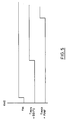
- FIG. 5 There is shown diagrammatically in FIG. 5 a chronogram of the flags TM, TBF1 and FNIF.
- the window defined by the flag DBF1 equals eight times the window defined by the flag TM, while the flag defined by FINF equals twice the flag defined by DBF1.
- the microcontroller has a TMIN / 8 time called dead time, during which the states it sends on the SM input are ignored. If at the end of this delay the SM input is not at zero, a RESET signal is generated. A re-initialization of the process is then restarted at the falling edge of the RESET.
- the microcontroller must maintain the SM input at zero between the validation of the TM flag and the validation of the DBF1 flag. If the entry SM however changes to one during this time window, a RESET pulse is generated and the reinitialization of the process is started.
- the microcontroller must deposit an impulse between the validation of the DBF1 flag and the validation of the FINF flag. If this is the case, the process of generation of the time windows by the counter 300 is reinitialized by validation of the reset signal at the moment when the pulse appears on SM. The function being considered as correct there is no generation of RESET pulse.
- the opening of the authorized period window is signaled at the output of the monitoring device by switching to one of the DBF output. When a re-initialization is carried out this output returns to zero.
- a RESET triggered by an oversized control signal on the SM input has the effect of switching the DFLT output to one. This output only goes back to zero if the microcontroller resumes a correct pulse generation. On power up the DFLT signal is initialized to zero.
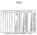
- the windows defined by the TM, DBF1 and FINF flags are functions of the frequency of the quartz used as input and of the inputs V1, V2, V3 and TL.
- the dead time window defined by the flag TM has a duration equal to TMIN / 8, TMIN being the lower limit of the authorized period, defined by the flag DBF1.
- the upper limit of the authorized period is 2TMIN if the TL input is zero and 4TMIN if the TL input is one.
- the width of the RESET pulse is equal to the period defined by the quartz divided by 256.
- the application represented in the appended FIG. 7 corresponds to monitoring the operation of a microcontroller in asynchronous mode.
- the inputs DR, TL, V3 and TEST of the CV device are placed at the low logic level while the inputs MV, V1 and V2 of the CV device are placed at the high logic level.
- the SDR input is connected to the midpoint of a bridge comprising a resistor R and a capacitor C in series between the ground and the positive supply terminal, the capacitor being placed on the ground side.
- a quartz crystal is connected to the OSLOW input of the circuit while the OSQUIC input is grounded.
- the circuit CV receives on its input SM the control signal generated by the microcontroller.
- the latter is controlled by the timing signal generated by the quartz, the HBUFF output of the CV device being connected to the microcontroller. Finally, if necessary, it is re-initialized thanks to the RESET signals generated by the CV circuit.
- the application represented in FIG. 8 corresponds to monitoring the operation of a microcontroller in synchronous mode, with monitoring of the operation of the monitoring device by the microcontroller.
- the application represented in FIG. 8 differs from that represented in FIG. 7 only by the fact that the input TL is placed at the high logic level and not at the low logic level on the one hand, and on the other hand and especially that the outputs DBF1 and SYNCRAZ of the CV monitoring device are connected to the microcontroller to indicate to the latter, by the DBF output, the validation of the flag of the minimum period, therefore the moment from which the microcontroller is authorized to place a pulse of the control signal, and indicate by the SYNCRAZ output that the CV monitoring device performs a reset zero of its counter 300 and therefore of the corresponding time windows.
- the application represented in FIG. 9 corresponds to monitoring the operation of a microcontroller with inhibition of the output interfaces thereof, from a fault detected in the operation of the microcontroller, until the return to normal operation of it.
- Figure 9 shows a CV monitoring device, a microcontroller and an output interface connected to the microcontroller.
- the application represented in FIG. 9 differs from that represented in FIG. 7 by the fact that on the one hand the input TL is at the high logic level and not at the low logic level and that on the other hand and above all the DFLT output of the CV monitoring device is connected to the inhibit input of the interface.
- the output DFLT of the circuit CV being at one as long as the period of the control signal leaves the authorized window, the output interface is inhibited as long as the operation of the microcontroller is abnormal.
- the application shown in Figure 10 corresponds to a periodic reset mode of the microcontroller.
- the input SM of the monitoring device CV does not receive the control signal from the microcontroller, but is placed at the low logic level.
- the counter 300 periodically abuts the maximum authorized period and validates the corresponding FINF flag. RESET pulses are thus generated periodically.
- the inputs and outputs of the CV monitoring device remain in accordance with the provisions described above with reference to FIG. 7, except that the input TL is again at the high logic level.
- the application represented in FIG. 11 corresponds to monitoring the operation of a microcontroller with the possibility of waking up a sleeping microcontroller by an external intervention, for example pressing a button or activating an infrared remote control receiver.
- FIG. 11 There is shown in Figure 11 attached a CV monitoring device receiving a quartz on its OSLOW input, a microcontroller, peripherals associated with motors, a key pressed detector, an infrared remote control receiver and a regulator.
- the regulator attacks the SDR input of the CV device.
- the DR input receives a logical combination of the output of external elements capable of waking the microcontroller, for example an infrared remote control receiver or a key detector pressed as indicated previously, so that a wake-up pulse is applied to the DR circuit CV input when activating one of these elements.
- the MV input of the CV monitoring device is connected to an output of the peripherals making it possible to indicate to the CV circuit whether or not the peripherals are energized.
- the TL, V1 and V2 inputs are at the high level.
- the V3 and TEST inputs are at the low level.
- the circuit CV receives on its input SM the control signal generated by the microcontroller.
- the RESET, HBUFF and HDIV outputs of the CV circuit are connected to the associated inputs of the microcontroller.
- the DFLT output of the CV monitoring device is connected to the inhibition input of the microcontroller's output devices.
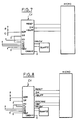
- the application represented in FIG. 12 corresponds to an application using a master microcontroller and a slave microcontroller with the possibility for the master microcontroller to fall asleep and wake up the functions of the slave microcontroller.
- FIG. 12 shows schematically a master microcontroller associated with a first CVM monitoring device, and a slave microcontroller associated with a second CVE monitoring device.
- FIG. 12 also schematically shows peripherals of the slave microcontroller.
- the inputs SDR, DR, NY, TL, V1, V2, V3, TEST, OSLOW and OSQUIC of the CVM device are connected as indicated above with reference to FIG. 8.
- the CVM circuit receives on its input SM the control signal from the microcontroller master. These RESET and HBUFF outputs are connected to the associated inputs of the master microcontroller. Its RESETB output is connected to the SDR input of the CVE circuit.
- the DR and MV inputs of the CVE circuit are connected to an associated terminal of the master microcontroller and to an authorization terminal of the peripherals of the slave microcontroller.
- the inputs TL, V1 and V2 of the CVE circuit are at the high logic level, the inputs V3, TEST and OSQUIC are at the low level a quartz attacks the OSLOW input.
- the CVE circuit receives on its SM input the control signal generated by the slave microcontroller. These RESET and HBUFF outputs are connected to the associated inputs of the slave microcontroller. Finally, the DFLT output of the CVE circuit attacks an associated terminal of the master microcontroller as well as the inhibition input of the peripherals.
- FIG. 13 shows a master microcontroller associated with a first CVM monitoring circuit, as well as a slave microcontroller associated with a second CVE monitoring circuit.
- FIG. 13 essentially differs from FIG. 12 by the absence of peripherals associated with the slave microcontroller. It follows that the output DFLT of the second monitoring device CVE is connected only to the master microcontroller and that the input DR of the device CVE is at low logic level while the input NV of the same circuit CVE is at high logic level.
Landscapes
- Engineering & Computer Science (AREA)
- Theoretical Computer Science (AREA)
- Physics & Mathematics (AREA)
- General Engineering & Computer Science (AREA)
- General Physics & Mathematics (AREA)
- Quality & Reliability (AREA)
- Debugging And Monitoring (AREA)
Claims (15)
- Vorrichtung zur Funktionsüberwachung eines Mikrosteuerbausteins oder Mikroprozessors, der ein Steuersignal SM erzeugt, mit:
einem Oszillator (100), welcher ein Taktungssignal konstanter und bekannter Frequenz liefert,
einem programmierbaren Frequenzteiler (200), welcher am Eingang das Taktungssignal erhält und an seinem Ausgang ein Taktsignal HC liefert, und
einem Zähler (300), der das Taktsignal HC erhält, dadurch gekennzeichnet, daß
der das Taktsignal HC erhaltende Zähler (300) drei Merker CM, DBF1, FINF für jeden Impuls des Steuersignals definiert, die jeweils einer bestimmten Anzahl von erhaltenen Taktimpulsen HC entsprechen,
wobei der Merker TM eine Totzeit repräsentiert, während welcher das Steuersignal SM irgendeinen Zustand annehmen kann,
der Merker DBF1 den minimalen zugelassenen Zeitabschnitt repräsentiert,
der Merker FINF den maximalen zugelassenen Zeitabschnitt repräsentiert,
und dadurch daß, sie ferner einen Ereigniskontrolleur (400) aufweist, welcher die Merker TM, DBF1, FINF und das Steuersignal SM erhält und überwacht, daß das Steuersignal SM
auf inaktivem Pegel während der Validierung des Merkers TM ist, um im gegenteiligen Fall ein RESET-Signal zu erzeugen,
vor Validierung des Merkers DBF1 nicht auf aktiven Pegel übergeht, um im gegenteiligen Fall ein RESET-Signal zu erzeugen,
zwischen der Validierung der Merker DBF1 und FINF auf aktiven Pegel übergeht, um eine Rücksetzung des Zählers (300) auf Null bei einer solchen Feststellung durchzuführen und um ein RESET-Signal zu erzeugen, wenn die Validierung des Merkers FINF vor dem Übergang des Steuersignals SM auf aktiven Pegel eintritt. - Überwachungsvorrichtung nach Anspruch 1, dadurch gekennzeichnet, daß der Frequenzteiler (200) eine Gruppe von in Kaskade geschalteten Kippgliedern (211 bis 218) zur Teilung des vom Oszillator (100) erzeugten Taktungssignals OSLOW und einen Aufbau von Logikgliedern aufweist, die einen Multiplexer (250) bilden, der eine logische Kombination der Ausgänge der Kippglieder (211 bis 218) und eines Programmierungsworts V1, V2, V3 zur Erzeugung des Taktsignals HC verwirklicht.
- Überwachungsvorrichtung nach Anspruch 2, dadurch gekennzeichnet, daß das Programmierungswort V1, V2, V3 drei Bits hat.
- Überwachungsvorrichtung nach einem der Ansprüche 1 bis 3, dadurch gekennzeichnet, daß der Frequenzteiler (200) ferner ein Hilfstaktsignal PHI1 liefert, dessen Frequenz derjenigen des Taktungssignals geteilt durch einen festen Wert entspricht.
- Überwachungsvorrichtung nach einem der Ansprüche 1 bis 4, dadurch gekennzeichnet, daß der Zähler (300) eine Gruppe von in Kaskade geschalteten Kippgliedern (301 bis 315) zur Teilung der Frequenz des Taktsignals HC und zur Speicherung des Kippens gewisser ausgewählter der Kippglieder (310, 313) geeignete Aufbauten (330, 331; 332, 333) aufweist.
- Überwachungsvorrichtung nach Anspruch 5, dadurch gekennzeichnet, daß die Speicheraufbauten zwei Logikglieder (330, 331; 332, 333) aufweisen.
- Überwachungsvorrichtung nach einem der Ansprüche 1 bis 6, dadurch gekennzeichnet, daß die Zeitdauer, welche die Validierung des den minimalen zugelassenen Zeitabschnitt repräsentierenden Merkers DBF1 von einer Rücksetzung auf Null trennt, ein Vielfaches der Zeitdauer ist, welche die Validierung des eine Totzeit repräsentierenden Merkers TM von der gleichen Rücksetzung auf Null trennt.
- Überwachungsvorrichtung nach Anspruch 7, dadurch gekennzeichnet, daß die Zeitdauer, welche die Validierung des Merkers DBF1 von einer Rücksetzung auf Null trennt, gleich dem Achtfachen der Zeitdauer ist, welche die Validierung des Merkers TM von der gleichen Rücksetzung auf Null trennt.
- Überwachungsvorrichtung nach einem der Ansprüche 1 bis 8, dadurch gekennzeichnet, daß die Zeitdauer, welche die Validierung des den maximalen zugelassenen Zeitabschnitt repräsentierenden Merkers FINF von einer Rücksetzung auf Null trennt, gleich einem Vielfachen der Zeitdauer ist, welche die Validierung des den minimalen zugelassenen Zeitabschnitt repräsentierenden Merkers DBF1 von der gleichen Rücksetzung auf Null trennt.
- Überwachungsvorrichtung nach Anspruch 9, dadurch gekennzeichnet, daß die Zeitdauer, welche die Validierung des Merkers FINF von einer Rücksetzung auf Null trennt gleich, wahlweise, dem Zwei- oder Vierfachen der Zeitdauer ist, welche die Validierung des Merkers DBF1 von der gleichen Rücksetzung auf Null trennt.
- Überwachungsvorrichtung nach Anspruch 10, dadurch gekennzeichnet, daß die Wahl der Zeitdauer des maximalen zugelassenen Zeitabschnitts durch Steuerung des logischen Zustands eines Eingangs TL der Schaltung durchgeführt wird.
- Überwachungsvorrichtung nach einem der Ansprüche 1 bis 11, dadurch gekennzeichnet, daß der Ereigniskontrolleur (400) Anschlüsse aufweist, welche eine logische Kombination des Steuersignals SM und der Merker TM, DBF1, FINF bilden.
- Überwachungsvorrichtung nach einem der Ansprüche 1 bis 12, dadurch gekennzeichnet, daß der Ereigniskontrolleur (400) einen Eingang SDR aufweist, der einen Prioritäts-RESET erzeugt.
- Überwachungsvorrichtung nach einem der Ansprüche 1 bis 13, dadurch gekennzeichnet, daß der Ereigniskontrolleur (400) einen Eingang MV aufweist, der zur Inhibierung der Überwachung des Steuersignals SM geeignet ist.
- Überwachungsvorrichtung nach Anspruch 14, dadurch gekennzeichnet, daß der Ereigniskontrolleur (400) einen Eingang DR aufweist, der für eine Erzeugung eines RESET-Signals, wenn der Eingang MV die Überwachung des Steuersignals SM inhibiert, geeignet ist.
Applications Claiming Priority (2)
| Application Number | Priority Date | Filing Date | Title |
|---|---|---|---|
| FR8908023 | 1989-06-16 | ||
| FR8908023A FR2648586B1 (fr) | 1989-06-16 | 1989-06-16 | Dispositif de surveillance du fonctionnement d'un microcontroleur ou microprocesseur |
Publications (2)
| Publication Number | Publication Date |
|---|---|
| EP0403396A1 EP0403396A1 (de) | 1990-12-19 |
| EP0403396B1 true EP0403396B1 (de) | 1994-03-02 |
Family
ID=9382814
Family Applications (1)
| Application Number | Title | Priority Date | Filing Date |
|---|---|---|---|
| EP19900401689 Expired - Lifetime EP0403396B1 (de) | 1989-06-16 | 1990-06-15 | Einrichtung zur Überwachung des Betriebs eines Mikrokontrollers oder Mikroprozessors |
Country Status (4)
| Country | Link |
|---|---|
| EP (1) | EP0403396B1 (de) |
| JP (1) | JPH0329036A (de) |
| DE (2) | DE69006930T4 (de) |
| FR (1) | FR2648586B1 (de) |
Families Citing this family (3)
| Publication number | Priority date | Publication date | Assignee | Title |
|---|---|---|---|---|
| DE19712375A1 (de) * | 1997-03-25 | 1998-10-01 | Bosch Gmbh Robert | Watchdog-Schaltung |
| EP1136830A1 (de) * | 2000-03-22 | 2001-09-26 | Infineon Technologies AG | Frequenzsensor für digitale Signale und Verfahren zur Frequenzüberwachung eines digitalen Signales |
| DE102007010886B3 (de) | 2007-03-06 | 2008-06-26 | Siemens Ag | Steuergerät für ein Fahrzeug |
Family Cites Families (4)
| Publication number | Priority date | Publication date | Assignee | Title |
|---|---|---|---|---|
| IT1117593B (it) * | 1979-01-24 | 1986-02-17 | Cselt Centro Studi Lab Telecom | Sistema di aotodiagnosi per una apparecchiatura di controllo gestita da elaboratore |
| DE2946081C3 (de) * | 1979-11-15 | 1995-09-21 | Wabco Vermoegensverwaltung | Schaltungsanordnung zur Überwachung der Funktion eines Mikroprozessors |
| US4705970A (en) * | 1985-02-04 | 1987-11-10 | American Telephone And Telegraph Company, At&T Bell Laboratories | Programmable interval timer with lock means |
| GB2197508A (en) * | 1986-11-03 | 1988-05-18 | Philips Electronic Associated | Data processing system with watchdog |
-
1989
- 1989-06-16 FR FR8908023A patent/FR2648586B1/fr not_active Expired - Lifetime
-
1990
- 1990-06-15 EP EP19900401689 patent/EP0403396B1/de not_active Expired - Lifetime
- 1990-06-15 DE DE1990606930 patent/DE69006930T4/de not_active Expired - Lifetime
- 1990-06-15 JP JP2155614A patent/JPH0329036A/ja active Pending
- 1990-06-15 DE DE1990606930 patent/DE69006930D1/de not_active Expired - Fee Related
Also Published As
| Publication number | Publication date |
|---|---|
| DE69006930D1 (de) | 1994-04-07 |
| DE69006930T2 (de) | 1994-10-13 |
| FR2648586A1 (fr) | 1990-12-21 |
| JPH0329036A (ja) | 1991-02-07 |
| FR2648586B1 (fr) | 1991-09-27 |
| DE69006930T4 (de) | 1995-06-14 |
| EP0403396A1 (de) | 1990-12-19 |
Similar Documents
| Publication | Publication Date | Title |
|---|---|---|
| EP0156752B1 (de) | Steuerungs- und Überwachungssystem für Notausgänge | |
| EP0252812B1 (de) | Sicherheitseinrichtung, die die Funktion einer elektronischen Einrichtung nach der ersten Unterbrechung ihrer elektrischen Speisung unterbindet | |
| EP0577220B1 (de) | Spielvorrichtung mit dauernd funktionierender Uhr | |
| JPH0353677B2 (de) | ||
| EP0203148A1 (de) | Wachhundzeitmessvorrichtung | |
| JPH0782589B2 (ja) | 侵入者検出装置 | |
| EP1293856A1 (de) | Geschützte integrierte Schaltung mit vertraulichen Teilen und Verfahren zur Aktivierung dieser Schaltung | |
| EP0441714A1 (de) | Einrichtung zur Überwachung des Betriebs eines Mikroprozessorsystems oder dergleichen | |
| US5828253A (en) | Phase synchronization system which reduces power consumption and high frequency noise | |
| EP0403396B1 (de) | Einrichtung zur Überwachung des Betriebs eines Mikrokontrollers oder Mikroprozessors | |
| EP0712641B1 (de) | Verfahren zum Einstellen eines elektrischen Parameters einer implantierbaren Vorrichtung und Vorrichtung zur Durchführung des Verfahrens | |
| EP0028178A1 (de) | Relais und Verfahren für die Fernsteuerung | |
| FR2594468A1 (fr) | Systeme de controle et de surveillance d'issues | |
| EP0460986B1 (de) | Zentralverriegelung für die Türen eines Autos | |
| EP0423663A1 (de) | Synchronisierte Uhr | |
| CA2214098C (fr) | Coupleur pour gerer une communication entre un support de donnees portable et un dispositif d'echange de donnees, et dispositif d'echange de donnees associe | |
| WO1999066467A1 (en) | Intelligent interface between lock system and alarm system | |
| FR2716765A1 (fr) | Procédé de reconnaisance de standard vidéo, et circuit mettant en Óoeuvre ce procédé. | |
| WO1998054428A1 (fr) | Dispositif de commande a redondance destine a equiper une serrure | |
| FR2741171A1 (fr) | Circuit electronique pour effectuer une remise a l'etat initial | |
| EP0881768A1 (de) | System und Verfahren zur Filterung eines Impulssignals | |
| FR2710765A1 (fr) | Circuit électronique de surveillance d'un processeur. | |
| JPH0792793B2 (ja) | マイクロコンピユ−タ | |
| EP0585513B1 (de) | Verfahrenssteuerungssystem mit Simultaneitätstabelle | |
| FR2742015A1 (fr) | Procede de securisation d'une action et dispositif de mise en oeuvre |
Legal Events
| Date | Code | Title | Description |
|---|---|---|---|
| PUAI | Public reference made under article 153(3) epc to a published international application that has entered the european phase |
Free format text: ORIGINAL CODE: 0009012 |
|
| AK | Designated contracting states |
Kind code of ref document: A1 Designated state(s): DE ES GB IT SE |
|
| 17P | Request for examination filed |
Effective date: 19910311 |
|
| 17Q | First examination report despatched |
Effective date: 19921201 |
|
| GRAA | (expected) grant |
Free format text: ORIGINAL CODE: 0009210 |
|
| AK | Designated contracting states |
Kind code of ref document: B1 Designated state(s): DE ES GB IT SE |
|
| PG25 | Lapsed in a contracting state [announced via postgrant information from national office to epo] |
Ref country code: GB Effective date: 19940302 Ref country code: ES Free format text: THE PATENT HAS BEEN ANNULLED BY A DECISION OF A NATIONAL AUTHORITY Effective date: 19940302 Ref country code: IT Free format text: LAPSE BECAUSE OF FAILURE TO SUBMIT A TRANSLATION OF THE DESCRIPTION OR TO PAY THE FEE WITHIN THE PRE;WARNING: LAPSES OF ITALIAN PATENTS WITH EFFECTIVE DATE BEFORE 2007 MAY HAVE OCCURRED AT ANY TIME BEFORE 2007. THE CORRECT EFFECTIVE DATE MAY BE DIFFERENT FROM THE ONE RECORDED.SCRIBED TIME-LIMIT Effective date: 19940302 Ref country code: SE Free format text: THE PATENT HAS BEEN ANNULLED BY A DECISION OF A NATIONAL AUTHORITY Effective date: 19940302 |
|
| REF | Corresponds to: |
Ref document number: 69006930 Country of ref document: DE Date of ref document: 19940407 |
|
| GBV | Gb: ep patent (uk) treated as always having been void in accordance with gb section 77(7)/1977 [no translation filed] |
Effective date: 19940302 |
|
| PLBE | No opposition filed within time limit |
Free format text: ORIGINAL CODE: 0009261 |
|
| STAA | Information on the status of an ep patent application or granted ep patent |
Free format text: STATUS: NO OPPOSITION FILED WITHIN TIME LIMIT |
|
| 26N | No opposition filed | ||
| PGFP | Annual fee paid to national office [announced via postgrant information from national office to epo] |
Ref country code: DE Payment date: 19960619 Year of fee payment: 7 |
|
| PG25 | Lapsed in a contracting state [announced via postgrant information from national office to epo] |
Ref country code: DE Free format text: LAPSE BECAUSE OF NON-PAYMENT OF DUE FEES Effective date: 19980303 |