EP0403016B1 - Semiconductor device comprising a control circuit and a power stage with vertical current flow, integrated in monolithic form in the same chip, and related manufacturing process - Google Patents
Semiconductor device comprising a control circuit and a power stage with vertical current flow, integrated in monolithic form in the same chip, and related manufacturing process Download PDFInfo
- Publication number
- EP0403016B1 EP0403016B1 EP90201505A EP90201505A EP0403016B1 EP 0403016 B1 EP0403016 B1 EP 0403016B1 EP 90201505 A EP90201505 A EP 90201505A EP 90201505 A EP90201505 A EP 90201505A EP 0403016 B1 EP0403016 B1 EP 0403016B1
- Authority
- EP
- European Patent Office
- Prior art keywords
- region
- type
- regions
- epitaxial layer
- transistor
- Prior art date
- Legal status (The legal status is an assumption and is not a legal conclusion. Google has not performed a legal analysis and makes no representation as to the accuracy of the status listed.)
- Expired - Lifetime
Links
Images


Classifications
-
- H—ELECTRICITY
- H10—SEMICONDUCTOR DEVICES; ELECTRIC SOLID-STATE DEVICES NOT OTHERWISE PROVIDED FOR
- H10D—INORGANIC ELECTRIC SEMICONDUCTOR DEVICES
- H10D84/00—Integrated devices formed in or on semiconductor substrates that comprise only semiconducting layers, e.g. on Si wafers or on GaAs-on-Si wafers
- H10D84/40—Integrated devices formed in or on semiconductor substrates that comprise only semiconducting layers, e.g. on Si wafers or on GaAs-on-Si wafers characterised by the integration of at least one component covered by groups H10D12/00 or H10D30/00 with at least one component covered by groups H10D10/00 or H10D18/00, e.g. integration of IGFETs with BJTs
- H10D84/401—Combinations of FETs or IGBTs with BJTs
-
- H—ELECTRICITY
- H10—SEMICONDUCTOR DEVICES; ELECTRIC SOLID-STATE DEVICES NOT OTHERWISE PROVIDED FOR
- H10D—INORGANIC ELECTRIC SEMICONDUCTOR DEVICES
- H10D84/00—Integrated devices formed in or on semiconductor substrates that comprise only semiconducting layers, e.g. on Si wafers or on GaAs-on-Si wafers
- H10D84/01—Manufacture or treatment
- H10D84/0107—Integrating at least one component covered by H10D12/00 or H10D30/00 with at least one component covered by H10D8/00, H10D10/00 or H10D18/00, e.g. integrating IGFETs with BJTs
-
- H—ELECTRICITY
- H10—SEMICONDUCTOR DEVICES; ELECTRIC SOLID-STATE DEVICES NOT OTHERWISE PROVIDED FOR
- H10D—INORGANIC ELECTRIC SEMICONDUCTOR DEVICES
- H10D84/00—Integrated devices formed in or on semiconductor substrates that comprise only semiconducting layers, e.g. on Si wafers or on GaAs-on-Si wafers
- H10D84/01—Manufacture or treatment
- H10D84/02—Manufacture or treatment characterised by using material-based technologies
- H10D84/03—Manufacture or treatment characterised by using material-based technologies using Group IV technology, e.g. silicon technology or silicon-carbide [SiC] technology
- H10D84/038—Manufacture or treatment characterised by using material-based technologies using Group IV technology, e.g. silicon technology or silicon-carbide [SiC] technology using silicon technology, e.g. SiGe
Definitions
- the present invention concerns a semiconductor device comprising a control circuit and a power stage with vertical current flow, integrated in monolithic form in a single chip, and the related manufacturing process.
- a semiconductor device comprising a control circuit and a power stage with vertical current flow, integrated in monolithic form in a single chip, and the related manufacturing process.
- BJT bipolar transistors
- Document "IEEE Transactions on Electron Devices 35 (1988) Oct. No 10, Part I, pages 1676-1682" discloses a Bipolar-Mode Field-Effect Transistor.
- Document EP-A-0 117 867 discloses a power transistor and a control transistor on a substrate.
- the purpose of the invention is to develop an integrated monolithic semiconductor device which, while maintaining the advantages above indicated, makes it possible to overcome the problems connected to the use of BJT and MOS power stages.
- n type epitaxial layer 2 is grown on an n+ type substrate 1 of monocrystalline silicon with a high concentration of impurities ( Fig.3 ).
- n type region 5 is obtained, extending over the whole area of the chip.
- p+ type regions 6 and 7 are formed.
- Fig. 4 shows how regions 6 extend from surface 8 to reach region 3 and to enclose an n type region 9, within which the NPN low voltage transistor will later be created, while regions 7 are destined to be used as the gate of the BMFET transistor.
- This process includes the following stages in sequence:
- the embodyment of the process illustrated in Figs. 8-12 offers two further advantages: the length of the channel (and therefore the blocking gain of the BMFET transistor) is increased, and it is also possible to set the doping concentration the first and second epitaxial layers independently, as the channel extends mainly in the first epitaxial layer, while the region of the epitaxial collector of the transistor of the control circuit is situated inside the second epitaxial layer: the doping levels of these two layers can, as a consequence, also be determined independently of each other.
- Fig.13 illustrates one possible embodiment. It regards the source region of the BMFET which could be made up of two regions 32 and 36 in series, if one wished to privilege the lower series drain resistance, instead of the blocking gain.
Landscapes
- Bipolar Integrated Circuits (AREA)
- Bipolar Transistors (AREA)
- Metal-Oxide And Bipolar Metal-Oxide Semiconductor Integrated Circuits (AREA)
- Junction Field-Effect Transistors (AREA)
Description
- The present invention concerns a semiconductor device comprising a control circuit and a power stage with vertical current flow, integrated in monolithic form in a single chip, and the related manufacturing process. The association on the same chip of a power stage realized with bipolar transistors (BJT) and the related control circuit, creates a very compact, efficient device, which has the following advantages over separate components:
- the reliability and the efficiency of the device increase, as it is possible to insert a series of dedicated controls (eg. "thermal shutdown", to switch-off the power stage when a certain maximum temperature is reached, "SOA" protection against direct secondary breakdowns, etc.), which, inasmuch as they are included on the same chip, are much more efficient than an external control;
- the cost of the system using a similar device is lower, as a single package is used instead of two (or more); this not only reduces the space and the weight of the system, but also increases overall reliability.
- On the other hand the use of BJT-type power stages makes it more difficult to solve other problems, such as, basically, the low switching speed, the maximum current density, the extension of the Reverse Bias Safe Operating Area (RBSOA). It is however a known fact that the use of power stages of the MOS type is only advisable for devices which can operate at low voltages, due to the problems connected to excessive series drain resistance (Ron).
- Document "IEEE Transactions on Electron Devices 35 (1988) Oct.
No 10, Part I, pages 1676-1682" discloses a Bipolar-Mode Field-Effect Transistor. Document EP-A-0 117 867 discloses a power transistor and a control transistor on a substrate. - The purpose of the invention is to develop an integrated monolithic semiconductor device which, while maintaining the advantages above indicated, makes it possible to overcome the problems connected to the use of BJT and MOS power stages.
- A semiconductor device according to the present invention is defined in
claim 1. A manufacturing process is defined inclaim 3. - This choice makes it possible to maximise the current handling, the ruggedness and the dynamic performances of the power stage. It also offers the following additional advantages:
- higher switching speed, and, as a result, lower power losses;
- higher current density, and therefore reduced area of the device;
- greater extension of the RBSOA area, and, as a result, reduced complexity of the driving circuit, as it is no longer necessary to protect the power stage while switching off inductive loads;
- easier design of the power stage, on account of the modular structure of the bipolar mode field effect transistor (BMFET) (in fact, since the BMFET transistor is made up of a plurality of identical elementary cells, a certain operating current is ensured simply by parallel connecting the required number of elementary cells).
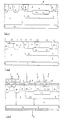
- The features of the invention may be better understood by the following description and the enclosed drawings, illustrating an example of non restrictive value, in which the various figures show:
- Fig.1:
- structure of a known device;
- Fig.2:
- structure of a similar device not covered by the invention;
- Figs.3, 4, 5, 6:
- first example of a manufacturing process of the device in Fig. 2;
- Fig.7:
- electrical equivalent of the structure in Fig. 6;
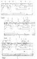
- Figs.8, 9, 10, 11, 12:
- manufacturing process of a device according to the invention;
- Fig.13:
- final structure of a device obtained with a variation to the process illustrated in Figs. 8-12.
- Fig. 1 illustrates the known structure of a semiconductor device comprising a control circuit and a power stage with vertical current flow, integrated in monolithic form on a single chip. For the sake of simplicity only one NPN transistor of the integrated control circuit (with emitter terminal = E, base terminal = B and collector = C), and one bipolar power transistor (with emitter terminal = E1, base terminal = B1 and collector = C1), have been indicated.
-
Regions - Fig.2 illustrates the structure of a similar device not covered by the invention. This structure differs from Fig. 1 in that the BJT power transistor is substitute by a BMFET transistor (with source terminal = S, gate terminal = G and drain terminal = D). The manufacturing process can be described as follows.
- An n type
epitaxial layer 2 is grown on ann+ type substrate 1 of monocrystalline silicon with a high concentration of impurities (Fig.3). - Using the usual techniques of oxidation, photomasking, implantation and diffusion, a
p+ type region 3 is formed, to constitute the horizontal isolation region of the components of the integrated control circuit and, within it, ann+ type region 4 is formed, destined to serve as buried collector layer of a transistor of the integrated control circuit. - At this point (Fig.4) a new epitaxial layer is grown, through which an
n type region 5 is obtained, extending over the whole area of the chip. Using the well known techniques of oxidation , photomasking, implantation and diffusion,p+ type regions - Fig. 4 shows how
regions 6 extend fromsurface 8 to reachregion 3 and to enclose ann type region 9, within which the NPN low voltage transistor will later be created, whileregions 7 are destined to be used as the gate of the BMFET transistor. - At this point (Fig.5)
regions - With well known techniques (Fig.6) the
base region 12 and theemitter region 13 of the NPN low voltage transistor are formed, contacts are realized and the various elements of the device are interconnected by a process of metallisation and photomasking. All the terminal electrodes of the various components are thus located on the front of the chip, except for the drain of the BMFET transistor which is on the back. - Fig.7 illustrates the electrical equivalent of the structure of Fig. 6 relating to the BMFET. It shows that the diode, whose anode is the isolation region, and whose cathode is the drain of the BMFET transistor, is reverse biased if terminal I is connected to the point of lowest potential among those present on the circuit; the components of the integrated pilot circuit are therefore isolated from each other and from the power stage.
- In Fig.6 it is clear that distance J between the lower edge of the isolation region and the substrate is lower than distance L between the lower edge of the gate region of the BMFET transistor and the substrate: as a result the breakdown voltage of the diode mentioned above is lower than the breakdown voltage of the BMFET transistor, and therefore the maximum operating voltage of the monolithic device corresponds to the first of these two. It is therefore necessary, at the design stage, to establish thickness J so that it can withstand the maximum required voltage. Since the current gain of the BMFET depends on the drain thickness, or L, according to a law of inverse quadratic proportionality, and since L > J, it can be seen that this gain is penalised by the different junction depth of the BMFET gate compared to that of the
horizontal isolation region 3. - It is therefore advantageous to devise a process which will make it possible to achieve L = J, as this will bring the current handling capability to a maximum, maintaining unchanged the device operating voltage. This equality is made possible by creating the BMFET gate region and the horizontal isolation region before the second epitaxial growth, using the same process of diffusion.
- An example of a process suitable to achieve this purpose is illustrated in Figs. 8, 9, 10, 11 and 12.
- This process includes the following stages in sequence:
- a first n type
epitaxial layer 15 is grown on asubstrate 14 of n+ type monocrystalline silicon with a high concentration of impurities; - with the usual techniques of oxidation, photomasking, implantation and diffusion,
regions layer 15, destined to constitute respectively the BMFET gate region and the horizontal isolation region of the integrated control circuit components; - an
n+ type region 18 is formed withinregion 17, in order to provide the buried collector layer of the transistor of the integrated control circuit; - a second epitaxial layer is grown creating an
n type region 19, which covers the whole surface of the chip; - using known techniques of oxidation, photomasking and implantation of the second epitaxial layer and successive diffusion,
regions regions 20 are immediately aboveregions 16 and join them,regions 21 extend fromsurface 22 up to reachregion 17; - two
n+ type regions region 23, constituting the source of the BMFET, is localised between twoadjacent regions 20 inside which it extends, whileregion 24, constituting the collector sink, is placed aboveregion 18 and joins it; - using well known techniques the
base region 25 and theemitter region 26 of the NPN low voltage transistor are made, the contacts are realized and the various elements of the device are interconnected by means of metallisation and photomasking process. - Fig.12 shows that the gate of the BMFET and the horizontal isolation region have the same junction depth.
- The embodyment of the process illustrated in Figs. 8-12 offers two further advantages: the length of the channel (and therefore the blocking gain of the BMFET transistor) is increased, and it is also possible to set the doping concentration the first and second epitaxial layers independently, as the channel extends mainly in the first epitaxial layer, while the region of the epitaxial collector of the transistor of the control circuit is situated inside the second epitaxial layer: the doping levels of these two layers can, as a consequence, also be determined independently of each other.
- It is clear that the examples of realisation described above can be modified, adapted or integrated, without going outside the scope of the present invention.
- Fig.13 illustrates one possible embodiment. It regards the source region of the BMFET which could be made up of two
regions - The relative manufacturing process foresees the following stages in sequence:
- a first n type epitaxial layer is grown on a
n+ type substrate 27 of monocrystalline silicon, with a high concentration of impurities; - using the usual techniques of oxidation, photomasking, implantation and diffusion,
p+ type regions layer 28, to constitute respectively the gate region of the BMFET and the horizontal isolation region of the components of the integrated control circuit; - an
n+ type region 31 is formed withinregion 29, to constitute the buried collector layer of the transistor of the integrated control circuit, and an n+ type region 32 (intended to be the source of the BMFET) situated between tworegions 30, inside which it extends; - a second epitaxial layer is grown, creating the
n type region 33, which covers the whole surface of the chip; - using known techniques of oxidation, photomasking and implantation of the second epitaxial layer and successive diffusion,
p+ type regions regions 35 are located immediately aboveregions 30 and join them,regions 34 extend from the upper surface of the second epitaxial layer down toregion 29; - two
n+ type regions region 36 is located immediately aboveregion 32 and joins it, whileregion 37 constitutes the collector sinker, is placed aboveregion 31 and joins it; - using well known techniques the
base region 38 and theemitter 39 of the NPN low voltage transistor are formed, the contacts are opened and the various elements of the device are interconnected using a process of metallisation and photomasking. - According to another possible variation, the
epitaxial region 5 in Fig. 6 could be formed by a double growth, or in such a way as to present a variable resistance. Another variation could be a double level of metallisation. - This double level of metallisation would be particularly advisable for the structure according to the invention, as it would permit a sensible reduction of space both for the power stage and for the control system. In fact for the metallisation tracks which collect the gate and source current of the BMFET, space could De saved which could be used to produce other elementary cells. In the same way it is possible to achieve higher component density in the region occupied by the control circuit.
Claims (4)
- Semiconductor device realized on an n+ type substrate (14,27) of monocrystalline silicon, comprising a power stage with vertical current flow and a control circuit containing at least one NPN low voltage transistor, integrated in monolithic form in a single chip, also including an isolation region to insulate the control circuit from the power stage and the components of the control circuit from each other, wherein the power stage consists of at least one BMFET transistor with the source terminal and the drain terminal situated on opposite sites of the chip and comprising- a first n type epitaxial layer (15,28) located on the n+ type substrate of monocrystalline silicon;- a second n type epitaxial layer (19,33) located on said first epitaxial layer,- a first p+ type region (17,29) inside said first epitaxial layer and constituting a horizontal isolation region of the integrated control circuit components;- second p+ type regions (16, 30) located inside said first n type epitaxial layer, laterally spaced from said first p+ type region and providing first gate regions of the BMFET ;- a second n+ type region (18,31) sinking inside said first p+ type region and constituting a buried collector layer of said low voltage transistor of the integrated control circuit;- third p+ type isolation regions (21,34) and fourth p+ type regions (20,35) inside the second epitaxial layer, said third regions being located over said first p+ type region and extending from the surface of the second epitaxial layer inside said second epitaxial layer to join said first p+ type region, and said fourth regions providing other gate regions of the BMFET transistor laterally spaced from said third regions and located immediately above said first gate regions and joining them;- a fifth n+ type region (23,36) and a sixth n+ type region (24,37), the fifth region, constituting a source region of the BMFET transistor, being located between two adjacent regions of said fourth regions inside which it partially extends, and the sixth region, constituting a collector sinker of the low voltage transistor, being positioned above said second n+ type region and joining it;- a base region (25,38) located in said first epitaxial layer and above said buried collector layer and an emitter region (26, 39) of the NPN low voltage transistor located in said base region;wherein the distance between the lower edge of the horizontal isolation region and the substrate is substantially the same as the distance between the lower edge of the first gate regions of the BMFET transistor and the substrate.
- Semiconductor device according to Claim 1, wherein the distance between the lower edge of the source region of the BMFET transistor and the substrate is substantially the same as the distance between the lower edge of the buried collector layer of the low voltage transistor and the substrate.
- Manufacturing process of a semiconductor device according to claim 1 comprising the following steps:- growing a first n type epitaxial layer (15,28) on an n+ type substrate (14,27) of monocrystalline silicon with a high concentration of impurities;- forming a first p+ type region (17,29) inside said first layer to constitute a horizontal isolation region of the integrated control circuit components;- forming second p+ type regions (16,30) inside said first layer, laterally spaced from said first p+ type region intended to provide first gate regions of the BMFET transistor;- forming a second n+ type region (18,31) sinking inside said first p+ type region, intended to provide a buried collector layer of said low voltage transistor of the integrated control circuit;- growing a second n type epitaxial layer (19,33) by which an n type region is obtained extending along the whole area of the chip;- forming third p+ type isolation regions (21,34) and fourth p+ type regions (20,35) inside the second epitaxial layer by using oxidation, photomasking, implantation and subsequent diffusion, said third regions being over said first p+ type region and extending from the surface of the second epitaxial layer inside said second epitaxial layer to join said first p+ type region, and said fourth regions being intended to provide other gate regions of the BMFET transistor laterally spaced from said third regions and located immediately above said first gate regions (16,30) and joining them;- forming a fifth n+ type region (23,36) and a sixth n+ type region (24,37), the fifth region, constituting a source region of the BMFET transistor, being located between two adjacent regions of said fourth regions inside which it partially extends, and the sixth region, constituting a collector sinker of the low voltage transistor, being positioned above said second n+ type region and joining it;- forming the base region (25,38) in said first epitaxial layer above said buried collector layer and the emitter region (26,39) of the NPN low voltage transistor in said base region;- realizing the contacts of the semiconductor device, and interconnecting the various elements of the device by metallisation and photomasking process.
- Manufacturing process of a semiconductor device according to Claim 3 wherein another n type source region (32) of the BMFET transistor is realized in the first epitaxial layer before the growth of the second epitaxial layer, said fifth region (36) being located immediately above said another source region and joining it.
Applications Claiming Priority (2)
| Application Number | Priority Date | Filing Date | Title |
|---|---|---|---|
| IT8906610A IT1234252B (en) | 1989-06-16 | 1989-06-16 | SEMICONDUCTOR DEVICE INCLUDING A CONTROL CIRCUIT AND A VERTICAL CURRENT FLOW POWER STAGE INTEGRATED IN A MONOLITHIC MODE IN THE SAME PLATE AND RELATED MANUFACTURING PROCESS |
| IT661089 | 1989-06-16 |
Publications (3)
| Publication Number | Publication Date |
|---|---|
| EP0403016A2 EP0403016A2 (en) | 1990-12-19 |
| EP0403016A3 EP0403016A3 (en) | 1991-12-04 |
| EP0403016B1 true EP0403016B1 (en) | 1997-10-22 |
Family
ID=11121377
Family Applications (1)
| Application Number | Title | Priority Date | Filing Date |
|---|---|---|---|
| EP90201505A Expired - Lifetime EP0403016B1 (en) | 1989-06-16 | 1990-06-12 | Semiconductor device comprising a control circuit and a power stage with vertical current flow, integrated in monolithic form in the same chip, and related manufacturing process |
Country Status (5)
| Country | Link |
|---|---|
| US (1) | US5119161A (en) |
| EP (1) | EP0403016B1 (en) |
| JP (1) | JP3083831B2 (en) |
| DE (1) | DE69031610T2 (en) |
| IT (1) | IT1234252B (en) |
Families Citing this family (7)
| Publication number | Priority date | Publication date | Assignee | Title |
|---|---|---|---|---|
| IT1217323B (en) * | 1987-12-22 | 1990-03-22 | Sgs Microelettronica Spa | INTEGRATED STRUCTURE OF HIGH VOLTAGE BIPOLAR POWER TRANSISTOR AND LOW VOLTAGE POWER MOS TRANSISTOR IN THE "EMITTER SWITCHING" CONFIGURATION AND RELATED MANUFACTURING PROCESS |
| USRE35642E (en) * | 1987-12-22 | 1997-10-28 | Sgs-Thomson Microelectronics, S.R.L. | Integrated high-voltage bipolar power transistor and low voltage MOS power transistor structure in the emitter switching configuration and relative manufacturing process |
| IT1246759B (en) * | 1990-12-31 | 1994-11-26 | Sgs Thomson Microelectronics | INTEGRATED STRUCTURE OF BIPOLAR POWER TRANSISTOR AND LOW VOLTAGE BIPOLAR TRANSISTOR IN '' EMITTER SWITCHING '' OR '' SEMI-BRIDGE '' CONFIGURATIONS AND RELATED MANUFACTURING PROCESSES. |
| DE69431181D1 (en) * | 1994-05-19 | 2002-09-19 | Cons Ric Microelettronica | Power integrated circuit ("PIC") and method of making the same |
| EP0751573A1 (en) * | 1995-06-30 | 1997-01-02 | STMicroelectronics S.r.l. | Integrated power circuit and corresponding manufacturing process |
| DE69931890T2 (en) | 1999-04-06 | 2007-01-11 | Stmicroelectronics S.R.L., Agrate Brianza | Integrated power circuit with vertical current flow and its manufacturing process |
| JP5048242B2 (en) * | 2005-11-30 | 2012-10-17 | オンセミコンダクター・トレーディング・リミテッド | Semiconductor device and manufacturing method thereof |
Family Cites Families (7)
| Publication number | Priority date | Publication date | Assignee | Title |
|---|---|---|---|---|
| GB1592856A (en) * | 1976-11-27 | 1981-07-08 | Ferranti Ltd | Semiconductor devices |
| EP0117867A4 (en) * | 1982-08-26 | 1985-04-23 | Mitsubishi Electric Corp | SEMICONDUCTOR ARRANGEMENT. |
| JPS60117765A (en) * | 1983-11-30 | 1985-06-25 | Fujitsu Ltd | Manufacture of semiconductor device |
| JPS63204640A (en) * | 1987-02-20 | 1988-08-24 | Hitachi Ltd | Semiconductor device and manufacture thereof |
| US4734382A (en) * | 1987-02-20 | 1988-03-29 | Fairchild Semiconductor Corporation | BiCMOS process having narrow bipolar emitter and implanted aluminum isolation |
| IT1221587B (en) * | 1987-09-07 | 1990-07-12 | S G S Microelettronics Spa | MANUFACTURING PROCEDURE OF AN INTEGRATED MONOLITHIC SEMICONDUCTOR DEVICE WITH LOW IMPURITY CONCENTRATION EPITAS LAYERS |
| IT1217322B (en) * | 1987-12-22 | 1990-03-22 | Sgs Microelettronica Spa | MANUFACTURING PROCEDURE OF A NON-LITHIC SEMICONDUCTIVE DEVICE INCLUDING AT LEAST A TRANSISTOR OF AN INTEGRATED CONTROL CIRCUIT AND A POWER TRANSISTOR IN TEGRATE IN THE SAME PLATE |
-
1989
- 1989-06-16 IT IT8906610A patent/IT1234252B/en active
-
1990
- 1990-06-12 EP EP90201505A patent/EP0403016B1/en not_active Expired - Lifetime
- 1990-06-12 DE DE69031610T patent/DE69031610T2/en not_active Expired - Fee Related
- 1990-06-14 JP JP02154121A patent/JP3083831B2/en not_active Expired - Fee Related
- 1990-06-14 US US07/537,940 patent/US5119161A/en not_active Expired - Lifetime
Also Published As
| Publication number | Publication date |
|---|---|
| EP0403016A2 (en) | 1990-12-19 |
| US5119161A (en) | 1992-06-02 |
| IT8906610A0 (en) | 1989-06-16 |
| IT1234252B (en) | 1992-05-14 |
| JP3083831B2 (en) | 2000-09-04 |
| JPH0342866A (en) | 1991-02-25 |
| EP0403016A3 (en) | 1991-12-04 |
| DE69031610D1 (en) | 1997-11-27 |
| DE69031610T2 (en) | 1998-03-12 |
Similar Documents
| Publication | Publication Date | Title |
|---|---|---|
| US5960277A (en) | Method of making a merged device with aligned trench FET and buried emitter patterns | |
| US5041895A (en) | Mixed technology integrated device comprising complementary LDMOS power transistors, CMOS and vertical PNP integrated structures having an enhanced ability to withstand a relatively high supply voltage | |
| US6657262B2 (en) | Monolithically integrated electronic device and fabrication process therefor | |
| US4862233A (en) | Integrated circuit device having vertical MOS provided with Zener diode | |
| US5162966A (en) | Semiconductor device having a surge protecting element | |
| US5372954A (en) | Method of fabricating an insulated gate bipolar transistor | |
| US5416354A (en) | Inverted epitaxial process semiconductor devices | |
| US20020053685A1 (en) | High side and low side guard rings for lowest parasitic performance in an H-bridge configuration | |
| US8420454B2 (en) | Three-terminal power device with high switching speed and manufacturing process | |
| EP0697739B1 (en) | Insulated gate bipolar transistor | |
| JPH06132525A (en) | High breakdown voltage MIS transistor and semiconductor device | |
| KR100683099B1 (en) | Semiconductor integrated circuit device and manufacturing method thereof | |
| US5654225A (en) | Integrated structure active clamp for the protection of power devices against overvoltages, and manufacturing process thereof | |
| JPH02275675A (en) | Mos type semiconductor device | |
| JPH07193154A (en) | Semiconductor integrated device | |
| EP0180255B1 (en) | Semiconductor device comprising a bipolar transistor and an insulated-gate fet | |
| JPH0758320A (en) | Insulated gate bipolar transistor | |
| US5530271A (en) | Integrated structure active clamp for the protection of power semiconductor devices against overvoltages | |
| JP2635044B2 (en) | Semiconductor device | |
| US5376821A (en) | Integrated emitter switching configuration using bipolar transistors | |
| US5119161A (en) | Semiconductor device comprising a control circuit and a power stage with a vertical current flow, integrated in monolithic form on a single chip | |
| US5246871A (en) | Method of manufacturing a semiconductor device comprising a control circuit and a power stage with a vertical current flow, integrated in monolithic form on a single chip | |
| JPS6233750B2 (en) | ||
| EP0459578B1 (en) | A monolithic semiconductor device and associated manufacturing process | |
| JP3932665B2 (en) | Semiconductor device |
Legal Events
| Date | Code | Title | Description |
|---|---|---|---|
| PUAI | Public reference made under article 153(3) epc to a published international application that has entered the european phase |
Free format text: ORIGINAL CODE: 0009012 |
|
| AK | Designated contracting states |
Kind code of ref document: A2 Designated state(s): DE FR GB NL |
|
| PUAL | Search report despatched |
Free format text: ORIGINAL CODE: 0009013 |
|
| AK | Designated contracting states |
Kind code of ref document: A3 Designated state(s): DE FR GB NL |
|
| 17P | Request for examination filed |
Effective date: 19920317 |
|
| 17Q | First examination report despatched |
Effective date: 19940526 |
|
| GRAG | Despatch of communication of intention to grant |
Free format text: ORIGINAL CODE: EPIDOS AGRA |
|
| GRAH | Despatch of communication of intention to grant a patent |
Free format text: ORIGINAL CODE: EPIDOS IGRA |
|
| GRAH | Despatch of communication of intention to grant a patent |
Free format text: ORIGINAL CODE: EPIDOS IGRA |
|
| GRAA | (expected) grant |
Free format text: ORIGINAL CODE: 0009210 |
|
| AK | Designated contracting states |
Kind code of ref document: B1 Designated state(s): DE FR GB NL |
|
| PG25 | Lapsed in a contracting state [announced via postgrant information from national office to epo] |
Ref country code: NL Free format text: LAPSE BECAUSE OF FAILURE TO SUBMIT A TRANSLATION OF THE DESCRIPTION OR TO PAY THE FEE WITHIN THE PRESCRIBED TIME-LIMIT Effective date: 19971022 |
|
| REF | Corresponds to: |
Ref document number: 69031610 Country of ref document: DE Date of ref document: 19971127 |
|
| ET | Fr: translation filed | ||
| NLV1 | Nl: lapsed or annulled due to failure to fulfill the requirements of art. 29p and 29m of the patents act | ||
| RAP4 | Party data changed (patent owner data changed or rights of a patent transferred) |
Owner name: STMICROELECTRONICS S.R.L. |
|
| PLBE | No opposition filed within time limit |
Free format text: ORIGINAL CODE: 0009261 |
|
| STAA | Information on the status of an ep patent application or granted ep patent |
Free format text: STATUS: NO OPPOSITION FILED WITHIN TIME LIMIT |
|
| 26N | No opposition filed | ||
| REG | Reference to a national code |
Ref country code: FR Ref legal event code: D6 |
|
| PGFP | Annual fee paid to national office [announced via postgrant information from national office to epo] |
Ref country code: FR Payment date: 20000612 Year of fee payment: 11 |
|
| PGFP | Annual fee paid to national office [announced via postgrant information from national office to epo] |
Ref country code: DE Payment date: 20000614 Year of fee payment: 11 |
|
| PGFP | Annual fee paid to national office [announced via postgrant information from national office to epo] |
Ref country code: GB Payment date: 20010718 Year of fee payment: 12 |
|
| REG | Reference to a national code |
Ref country code: GB Ref legal event code: IF02 |
|
| PG25 | Lapsed in a contracting state [announced via postgrant information from national office to epo] |
Ref country code: FR Free format text: LAPSE BECAUSE OF NON-PAYMENT OF DUE FEES Effective date: 20020228 |
|
| PG25 | Lapsed in a contracting state [announced via postgrant information from national office to epo] |
Ref country code: DE Free format text: LAPSE BECAUSE OF NON-PAYMENT OF DUE FEES Effective date: 20020403 |
|
| PG25 | Lapsed in a contracting state [announced via postgrant information from national office to epo] |
Ref country code: GB Free format text: LAPSE BECAUSE OF NON-PAYMENT OF DUE FEES Effective date: 20020612 |
|
| GBPC | Gb: european patent ceased through non-payment of renewal fee |
Effective date: 20020612 |