EP0401654B1 - Device for coupling and/or uncoupling of light beams with an integrated optical element - Google Patents
Device for coupling and/or uncoupling of light beams with an integrated optical element Download PDFInfo
- Publication number
- EP0401654B1 EP0401654B1 EP90110217A EP90110217A EP0401654B1 EP 0401654 B1 EP0401654 B1 EP 0401654B1 EP 90110217 A EP90110217 A EP 90110217A EP 90110217 A EP90110217 A EP 90110217A EP 0401654 B1 EP0401654 B1 EP 0401654B1
- Authority
- EP
- European Patent Office
- Prior art keywords
- coupling
- grating
- photoelectric device
- diffraction
- integrated optical
- Prior art date
- Legal status (The legal status is an assumption and is not a legal conclusion. Google has not performed a legal analysis and makes no representation as to the accuracy of the status listed.)
- Expired - Lifetime
Links
- 230000003287 optical effect Effects 0.000 title claims abstract description 24
- 230000008878 coupling Effects 0.000 title claims abstract description 18
- 238000010168 coupling process Methods 0.000 title claims abstract description 18
- 238000005859 coupling reaction Methods 0.000 title claims abstract description 18
- 238000005286 illumination Methods 0.000 claims 2
- 238000005259 measurement Methods 0.000 abstract description 2
- 239000013307 optical fiber Substances 0.000 description 3
- 239000000758 substrate Substances 0.000 description 3
- 238000005516 engineering process Methods 0.000 description 1
- 230000002452 interceptive effect Effects 0.000 description 1
- 238000004519 manufacturing process Methods 0.000 description 1
Images


Classifications
-
- G—PHYSICS
- G02—OPTICS
- G02B—OPTICAL ELEMENTS, SYSTEMS OR APPARATUS
- G02B6/00—Light guides; Structural details of arrangements comprising light guides and other optical elements, e.g. couplings
- G02B6/10—Light guides; Structural details of arrangements comprising light guides and other optical elements, e.g. couplings of the optical waveguide type
- G02B6/12—Light guides; Structural details of arrangements comprising light guides and other optical elements, e.g. couplings of the optical waveguide type of the integrated circuit kind
- G02B6/122—Basic optical elements, e.g. light-guiding paths
- G02B6/124—Geodesic lenses or integrated gratings
-
- G—PHYSICS
- G01—MEASURING; TESTING
- G01D—MEASURING NOT SPECIALLY ADAPTED FOR A SPECIFIC VARIABLE; ARRANGEMENTS FOR MEASURING TWO OR MORE VARIABLES NOT COVERED IN A SINGLE OTHER SUBCLASS; TARIFF METERING APPARATUS; MEASURING OR TESTING NOT OTHERWISE PROVIDED FOR
- G01D5/00—Mechanical means for transferring the output of a sensing member; Means for converting the output of a sensing member to another variable where the form or nature of the sensing member does not constrain the means for converting; Transducers not specially adapted for a specific variable
- G01D5/26—Mechanical means for transferring the output of a sensing member; Means for converting the output of a sensing member to another variable where the form or nature of the sensing member does not constrain the means for converting; Transducers not specially adapted for a specific variable characterised by optical transfer means, i.e. using infrared, visible, or ultraviolet light
- G01D5/32—Mechanical means for transferring the output of a sensing member; Means for converting the output of a sensing member to another variable where the form or nature of the sensing member does not constrain the means for converting; Transducers not specially adapted for a specific variable characterised by optical transfer means, i.e. using infrared, visible, or ultraviolet light with attenuation or whole or partial obturation of beams of light
- G01D5/34—Mechanical means for transferring the output of a sensing member; Means for converting the output of a sensing member to another variable where the form or nature of the sensing member does not constrain the means for converting; Transducers not specially adapted for a specific variable characterised by optical transfer means, i.e. using infrared, visible, or ultraviolet light with attenuation or whole or partial obturation of beams of light the beams of light being detected by photocells
- G01D5/36—Forming the light into pulses
- G01D5/38—Forming the light into pulses by diffraction gratings
-
- G—PHYSICS
- G02—OPTICS
- G02B—OPTICAL ELEMENTS, SYSTEMS OR APPARATUS
- G02B6/00—Light guides; Structural details of arrangements comprising light guides and other optical elements, e.g. couplings
- G02B6/24—Coupling light guides
- G02B6/26—Optical coupling means
- G02B6/34—Optical coupling means utilising prism or grating
Definitions
- Vertical incident partial beams 51 'and 51 ⁇ also meet in this example circular gratings 53 and 54 which they lead to a coupler 59 in the indicated optical fibers 57 and 58.
Abstract
Description
Die Erfindung bezieht sich auf eine lichtelektrische Vorrichtung gemäß dem Oberbegriff des Anspruches 1.The invention relates to a photoelectric device according to the preamble of
Derartige Vorrichtungen werden in zunehmendem Maße in der Längen- und Winkelmeßtechnik angewandt, um möglichst klein bauende und störungsunanfällige Positionsmeßeinrichtungen herstellen zu können.Devices of this type are increasingly being used in length and angle measurement technology in order to be able to produce position measuring devices which are as small as possible and are not susceptible to faults.
Eine miniaturisierte Positionsmeßeinrichtung ist beispielsweise Gegenstand der DE 36 25 327 C1. Aus dieser Druckschrift, sowie aus dem dort genannten Stand der Technik ist es prinzipiell bekannt, mit Hilfe von Einkoppelgittern Licht in Lichtwellenleiter von integrierten optischen Schaltungen einzuspeisen.A miniaturized position measuring device is, for example, the subject of
Aus dem Stand der Technik ist ferner zu entnehmen, daß Ein- oder auch Auskoppelgitter komplizierten mathematischen Zusammenhängen unterliegen und meistens elliptisch oder parabolisch verlaufen, oder noch komplizierter aufgebaut sind.It can also be seen from the prior art that coupling-in or coupling-out gratings are subject to complicated mathematical relationships and are usually elliptical or parabolic, or are even more complicated.
Das hat zur Folge, daß in der Praxis bisher kaum Geräte realisiert worden sind, in denen real gefertigte Gitter zum Ein- oder Auskoppeln vorhanden sind, obwohl der Bedarf an derartig miniaturisierten Positionsmeßeinrichtungen besteht. In der EP-A 0 276 395 ist eine derartige Vorrichtung beschrieben. Von dieser Druckschrift geht die Erfindung aus.The consequence of this is that, in practice, hardly any devices have been implemented in which actually manufactured grids for coupling in or out are present, although there is a need for such miniaturized position measuring devices. Such a device is described in EP-A 0 276 395. The invention is based on this document.
Der Erfindung liegt demgemäß die Aufgabe zugrunde, eine Vorrichtung der eingangs genannten Art anzugeben, bei der die Abstimmung der einzuspeisenden Lichtstrahlen und der Einkoppelgitter bzw. der Auskoppelgitter und der auszukoppelnden Lichtstrahlen so erfolgt, daß sich eine einfache Gitterstruktur ergibt.The invention is accordingly based on the object of specifying a device of the type mentioned in the introduction, in which the tuning of the light beams to be fed in and the coupling-in grating or the coupling-out grating and the light beams to be coupled out takes place in such a way that a simple grating structure results.
Diese Aufgabe wird von einer Vorrichtung mit den Merkmalen des Anspruches 1 gelöst.This object is achieved by a device with the features of
Die besonderen Vorteile der Erfindung liegen darin, daß sich Zirkulargitter relativ einfach fertigen lassen und daß sich integriert-optische Bausteine gemäß der Erfindung sehr gut bei Positionsmeßeinrichtungen einsetzen lassen.The particular advantages of the invention are that circular gratings can be manufactured relatively easily and that integrated optical modules according to the invention can be used very well in position measuring devices.
Vorteilhafte Ausgestaltungen der Erfindung sind den Unteransprüchen zu entnehmen.Advantageous embodiments of the invention can be found in the subclaims.
Mit Hilfe von Ausführungsbeispielen soll die Erfindung anhand der Zeichnungen noch näher erläutert werden.With the help of exemplary embodiments, the invention will be explained in more detail with reference to the drawings.
Es zeigt
Figur 1 einen schematisierten Ausschnitt einer Positionsmeßeinrichtung nach dem Stand der Technik,- Figur 2 eine erfindungsgemäße Auflicht-Meßeinrichtung,
Figur 3 eine schematische Seitenansicht einer Auflicht-Meßeinrichtung mit einer Gitterkonstante GK 1,Figur 4 eine schematische Seitenansicht einer Auflicht-Meßeinrichtung mit einer Gitterkonstante GK 2,Figur 5 eine Durchlicht-Meßeinrichtung,- Figur 6 eine Durchlicht-Meßeinrichtung mit integrierten Linear- und Zirkulargittern,
- Figur 7 eine schematische Seitenansicht einer Meßeinrichtung gemäß Figur 6 aber mit Auflichtmaßstab und
- Figur 8 eine Meßeinrichtung mit zirkularem Auskoppelgitter.
- FIG. 1 shows a schematic section of a position measuring device according to the prior art,
- FIG. 2 an incident light measuring device according to the invention,
- FIG. 3 shows a schematic side view of an incident light measuring device with a grating
constant GK 1, - FIG. 4 shows a schematic side view of an incident light measuring device with a grating constant GK 2,
- FIG. 5 a transmitted light measuring device,
- FIG. 6 shows a transmitted light measuring device with integrated linear and circular gratings,
- Figure 7 is a schematic side view of a measuring device according to Figure 6 but with reflected light and
- 8 shows a measuring device with a circular coupling-out grating.
Beim in Figur 1 gezeigten Stand der Technik fällt ein Lichtstrahl 1 senkrecht auf einen als Beugungsgitter 2 ausgebildeten Maßstab einer Positionsmeßeinrichtung. Am Maßstab 2 wird der Lichtstrahl 1 gebeugt und zwei symmetrische Strahlenbündel 1′ und 1˝ werden auf zwei Einkoppelgitter 3 und 4 gelenkt, die Bestandteile eines integriert-optischen Bausteines 5 sind.In the prior art shown in FIG. 1, a
Die Einkoppelgitter 3 und 4 sind im weitesten Sinne parabolisch, wie in der eingangs zitierten DE 36 25 327 C1 noch näher angegeben ist. Während das Beugungsgitter 2 mit Gitterkonstanten zwischen 1,5 µm bis 20 µm realisiert werden kann, weisen die Einkoppelgitter 3 und 4 Gitterkonstanten in der Größenordnung von 0,5 µm auf. Daher lassen sie sich bei der notwendigerweise komplizierten Form nur mit sehr hohem Aufwand herstellen.The
Gemäß Figur 2 fällt ein Lichtstrahl 21 von der Rückseite her auf ein Beugungsgitter 26, das Bestandteil eines integriert-optischen Bausteines 25 ist. An diesem Beugungsgitter 26 wird der Lichtstrahl 21 gebeugt und zwei symmetrische Teilstrahlenbündel 21′ und 21˝ werden auf einen Gitter-Maßstab 22 einer erfindungsgemäßen Positionsmeßeinrichtung gelenkt. Das Beugungsgitter 26 und der Gitter-Maßstab 22 haben die gleiche Gitterkonstante. Vom Gitter-Maßstab 22 werden die Teilstrahlenbündel 21′ und 21˝ reflektiert und nochmals gebeugt, so daß sie unter rechten Winkeln auf den integriert-optischen Baustein 25 treffen. An den Auftreffbereichen der Teilstrahlenbündel 21′ und 21˝According to FIG. 2, a
weist der integriert-optische Baustein 25 zwei Einkoppelgitter 23 und 24 auf, die als sogenannte Zirkulargitter ausgebildet sind. Zirkulargitter sind verhältnismäßig einfach auch mit der erforderlichen geringen Gitterkonstante von ca. 0,5 µm herstellbar.the integrated
Wesentlich für die Funktion des Einkoppelns mittels der Zirkulargitter 23, 24 ist der senkrechte Einfall der Teilstrahlenbündel 21′ und 21˝. Dies wird erreicht durch die Gleichheit der Gitterkonstanten des Beugungsgitters 26 und des Gitter-Maßstabes 22.The vertical is essential for the function of the coupling by means of the
Die eingekoppelten Teilstrahlenbündel 21′ und 21˝ werden mittels planaren Lichtwellenleitern 27, 28 einem an sich bekannten Koppler 29 zugeführt, durch den sie zur Interferenz miteinander gebracht werden. Mit Hilfe von Detektoren 210, 211 und (nicht gezeigt 212) können die interferierenden Teilstrahlenbündel in zueinander phasenverschobene elektrische Signale umgewandelt werden. Dabei können die Detektoren 210, 211, 212 Bestandteile des integriert-optischen Bausteines 25 sein.The coupled
In Figur 3 bzw. 4 werden Prinzip-Ansichten von Meßeinrichtungen gemäß Figur 2 gezeigt. Daraus wird deutlich, daß für einen geeigneten (senkrecht auf die Einkoppelgitter 33, 34 bzw. 43, 44 auftreffenden) Strahlenverlauf nicht die Gitterkonstante der Beugungsgitter 36 bzw. 46 und der Gitter-Maßstäbe 32 bzw. 42 entscheidend ist, sondern nur jeweils deren Gleichheit. Durch die Wahl der jeweiligen Gitterkonstanten kann der Beugungswinkel α1 bzw. α2 und somit der Abstand der Gitter voneinander bestimmt werden.3 and 4 show principle views of measuring devices according to FIG. 2. It is clear from this that it is not the grating constant of the
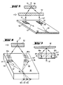
Figur 5 zeigt eine Variante, bei der ein Beugungsgitter 56 nicht integrierter Bestandteil eines optisch-integrierten Bausteines 55 ist. Hier sind sowohl das Beugungsgitter 56 als auch ein Gitter-Maßstab 52 als Durchlichtgitter - wieder mit gleicher Gitterkonstante - ausgebildet.FIG. 5 shows a variant in which a diffraction grating 56 is not an integral part of an optically integrated
Senkrecht einfallende Teilstrahlenbündel 51′ und 51˝ treffen auch in diesem Beispiel auf Zirkulargitter 53 und 54 die sie in angedeuteten Lichtwellenleitern 57 und 58 einem Koppler 59 zuleiten.Vertical incident
Ein weiteres Ausführungsbeispiel zeigt Figur 6, bei dem an einem Gitter-Maßstab 62 ein einfallender Lichtstrahl 61 so gebeugt wird, daß zwei symmetrische Teilstrahlenbündel 61′ und 61˝ auf zwei Beugungsgitter 66a und 66b auftreffen, die wiederum die gleiche Gitterkonstante aufweisen, wie der Gitter-Maßstab 62. Die beiden Beugungsgitter 66a und 66b sind integrierter Bestandteil eines optisch-integrierten Bausteines 65 und befinden sich auf dessen dem Gitter-Maßstab 62 zugewandten Oberseite. An den Beugungsgittern 66a und 66b werden die Teilstrahlenbündel 61′ und 61˝ so gebeugt, daß sie senkrecht auf zwei Zirkular-Einkoppelgitter 63, 64 fallen, die sich auf der Unterseite des integriert-optischen Bausteines 65 befinden. Dort befinden sich auch die angedeuteten Lichtwellenleiter 67 und 68 sowie ein Koppler 69 und drei Detektoren 610, 611 und 612.Another embodiment is shown in FIG. 6, in which an
In Figur 7 ist eine Seitenansicht der Anordnung gemäß Figur 6 dargestellt, sodaß für gleiche Elemente auch gleiche Bezugszeichen eingesetzt wurden. In dieser Figur 7 soll nur verdeutlicht werden, daß sich die Beugungsgitter 66a, 66b und die Einkoppelgitter 63, 64 auf den Oberflächen des Substrates des integriert-optischen Bausteines 65 gegenüber liegen. Allerdings weicht die Anordnung gemäß Figur 7 von der gemäß Figur 6 dadurch ab, daß der Eingangs-Lichtstrahl 61 durch das Substrat des integriert-optischen Bausteines 65 hindurch geführt und am Gitter-Maßstab 62 gebeugt und reflektiert wird.FIG. 7 shows a side view of the arrangement according to FIG. 6, so that the same reference numerals have been used for the same elements. In FIG. 7, it should only be clarified that the
In Figur 8 ist schließlich ein Ausschnitt einer Positionsmeßeinrichtung gezeigt, bei der auch eine nicht dargestellte Lichtquelle integrierter Bestandteil des integriert-optischen Bausteines 85 ist. Der Beleuchtungsstrahl 81 wird mittels eines Lichtwellenleiters 81a in ein Auskoppelgitter 81b eingespeist. Analog zu den bereits in den anderen Ausführungsbeispielen erläuterten zirkularen Einkoppelgittern (die auch hier unter den Bezugszeichen 83 und 84 eingesetzt sind), ist das Auskoppelgitter 81b als Zirkulargitter ausgebildet, so daß der Lichtstrahl 81 senkrecht ausgekoppelt, auf einen Gitter-Maßstab 82 trifft, dort gebeugt und reflektiert wird. Die gebeugten Teilstrahlenbündel 81′ und 81˝ treffen auf Beugungsgitter 86a und 86b, an denen sie wiederum gebeugt werden. Die Beugungsgitter 86a und 86b sind integrierte Bestandteile des integriert-optischen Bausteins 85, denen auf der Unterseite des Substrates die bereits erwähnten Einkoppelgitter 83 und 84 gegenüberliegen, in die die Teilstrahlenbündel senkrecht eingespeist werden.Finally, FIG. 8 shows a section of a position measuring device in which a light source, not shown, is also an integral part of the integrated optical module 85. The
In der bereits zu Figur 6 beschriebenen Weise können daraus wieder zueinander phasenverschobene elektrische Signale gewonnen werden.In the manner already described for FIG. 6, electrical signals which are out of phase with respect to one another can be obtained from this.
Am letzten Beispiel soll deutlich werden, daß grundsätzlich Ein- und Auskoppelgitter als gleichrangig angesehen werden.The last example should make it clear that coupling-in and coupling-out gratings are considered to be of equal importance.
Claims (10)
- A photoelectric device for coupling in and/or coupling out light beams with an integrated optical component (5, 25, 35, 45, 55, 65, 85), with a source of illumination and at least one first diffraction element (2, 26, 36, 46, 62, 82) for generating at least one diffracted bundle of rays (21′ to 81˝), as well as with at least one coupling in and/or coupling out element (3, 4, 23, 24, 33, 34, 43, 44, 53, 54, 63, 64, 83, 84) for coupling in and/or coupling out the diffracted bundle of rays (21′ to 81˝) into and/or out of an optical waveguide (27, 28, 57, 58, 67, 68, 81a), characterized in that the coupling in and/or coupling out element is formed from a circular grating (23 to 84) and in that at least one further diffraction element (22 to 82) is provided and is so matched to the first diffraction element (26 to 86b) that the diffracted bundle of rays (21′ to 81˝) enters into the circular grating (23 to 84) perpendicular thereto or emerges from the circular grating (81a) perpendicular thereto.
- A photoelectric device according to claim 1, characterized in that the first diffracting element is formed as a diffraction grating (26 to 82), at which two symmetrical component bundles of rays (21′ to 81˝) are generated, and in that the further diffracting element is likewise formed as a diffraction grating (22 to 86b), whose grating constant matches that of the first diffraction grating (26 to 82), so that the diffracted component bundles of rays (21′ to 81˝) enter into two circular gratings (23 to 84) perpendicular thereto.
- A photoelectric device according to claim 2, characterized in that one of the diffraction gratings (22 to 82) represents a measuring element of a photoelectric position measuring device.
- A photoelectric device according to claim 3, characterized in that the measuring element (22 to 82) and the further diffraction grating (26 to 86b) are formed as linear gratings.
- A photoelectric device according to claim 3, characterized in that the measuring element is formed as a radial grating.
- A photoelectric device according to claim 4, characterized in that the circular grating (23 to 84) and at least one of the diffraction gratings (26 to 86b) are component of an integrated optical component (25 to 85).
- A photoelectric device according to claim 6, characterized in that the integrated optical component (25 to 85) has a coupler (29 to 69) in which the coupled in component bundles of rays (21′ to 81˝) are brought into interference, detected by detectors (210 to 612) and converted into mutually phase-displaced electric signals.
- A photoelectric device according to claim 7, characterized in that the detectors (210 to 612) are integrated components of the integrated optical component (25 to 85).
- A photoelectric device according to claim 6, characterized in that the integrated optical component also comprises the source of illumination.
- A photoelectric device according to claim 6, characterized in that the illuminating ray path (81) in an optical waveguide (81a) is fed into a coupling-out circular grating (81b) which so deflects it that it emerges perpendicularly on to the measuring element (82).
Priority Applications (1)
| Application Number | Priority Date | Filing Date | Title |
|---|---|---|---|
| AT90110217T ATE85705T1 (en) | 1989-06-08 | 1990-05-30 | DEVICE FOR COUPLING AND/OR COUPLING LIGHT BEAM WITH AN INTEGRATED OPTICAL COMPONENT. |
Applications Claiming Priority (2)
| Application Number | Priority Date | Filing Date | Title |
|---|---|---|---|
| DE3918726 | 1989-06-08 | ||
| DE3918726A DE3918726C1 (en) | 1989-06-08 | 1989-06-08 |
Publications (3)
| Publication Number | Publication Date |
|---|---|
| EP0401654A2 EP0401654A2 (en) | 1990-12-12 |
| EP0401654A3 EP0401654A3 (en) | 1991-03-27 |
| EP0401654B1 true EP0401654B1 (en) | 1993-02-10 |
Family
ID=6382358
Family Applications (1)
| Application Number | Title | Priority Date | Filing Date |
|---|---|---|---|
| EP90110217A Expired - Lifetime EP0401654B1 (en) | 1989-06-08 | 1990-05-30 | Device for coupling and/or uncoupling of light beams with an integrated optical element |
Country Status (5)
| Country | Link |
|---|---|
| US (1) | US5127733A (en) |
| EP (1) | EP0401654B1 (en) |
| JP (1) | JPH07119854B2 (en) |
| AT (1) | ATE85705T1 (en) |
| DE (2) | DE3918726C1 (en) |
Cited By (1)
| Publication number | Priority date | Publication date | Assignee | Title |
|---|---|---|---|---|
| EP3792668B1 (en) * | 2019-09-10 | 2021-12-15 | Sick Ag | Optoelectronic sensor and method for detecting objects in a surveillance area |
Families Citing this family (18)
| Publication number | Priority date | Publication date | Assignee | Title |
|---|---|---|---|---|
| DE4013566A1 (en) * | 1990-04-27 | 1991-11-07 | Heidenhain Gmbh Dr Johannes | Photoelectric angle-measuring device esp. for machine tool |
| KR100254024B1 (en) * | 1990-07-23 | 2000-06-01 | 가나이 쓰도무 | Method of position detection and method and apparatus of printing patterns by use of the position detection method |
| ATE108897T1 (en) * | 1991-05-24 | 1994-08-15 | Heidenhain Gmbh Dr Johannes | DEVICE FOR COUPLING AND/OR COUPLING LIGHT BEAM WITH AN INTEGRATED OPTICAL COMPONENT. |
| DE4205750A1 (en) * | 1992-02-25 | 1993-08-26 | Siemens Ag | Optical frequency demultiplexer for optical fibre information transmission - has detector array components outside layer plane of waveguide provided with semiconductor amplifier and grating |
| DE4209672C1 (en) * | 1992-03-25 | 1993-07-08 | Deutsche Aerospace Ag, 8000 Muenchen, De | Wavelength measuring device for spectrometry - has sandwich structure of optical waveguides with diffraction gratings of differing constant giving spatial separation of components |
| JP3210111B2 (en) * | 1992-12-24 | 2001-09-17 | キヤノン株式会社 | Displacement detector |
| DE4302313C2 (en) * | 1993-01-28 | 1996-12-05 | Heidenhain Gmbh Dr Johannes | Multi-coordinate measuring device |
| EP0625690B1 (en) * | 1993-05-21 | 1996-04-03 | Dr. Johannes Heidenhain GmbH | Optoelectric position measuring device |
| US5507455A (en) * | 1993-12-28 | 1996-04-16 | Yang; Ro-King | Automatic control device for flying state of remote-control toy airplane |
| EP0770219B1 (en) * | 1994-07-08 | 1999-10-20 | Forskningscenter Riso | An optical measurement method and apparatus |
| DE19726397A1 (en) * | 1997-06-21 | 1998-12-24 | Heidenhain Gmbh Dr Johannes | Reticle and optical device with an illuminable reticle |
| US7129508B2 (en) * | 2002-01-18 | 2006-10-31 | Honeywell International Inc. | Compact VCSEL sensor with multiple sensing capabilities |
| JP2011107384A (en) * | 2009-11-17 | 2011-06-02 | Nec Corp | Method for manufacturing optical coupling device |
| US9162404B2 (en) * | 2011-03-05 | 2015-10-20 | Alcatel Lucent | Radial optical coupler |
| US8682120B2 (en) | 2011-03-05 | 2014-03-25 | Alcatel Lucent | Polarization-independent grating optical coupler |
| US9140854B2 (en) | 2011-09-22 | 2015-09-22 | Alcatel Lucent | Spatial division multiplexing optical mode converter |
| DE102019102488A1 (en) * | 2019-01-31 | 2020-08-06 | Rheinmetall Waffe Munition Gmbh | Device for combining at least two laser beams |
| WO2020209855A1 (en) * | 2019-04-11 | 2020-10-15 | Hewlett-Packard Development Company, L.P. | Three dimensional imaging |
Family Cites Families (18)
| Publication number | Priority date | Publication date | Assignee | Title |
|---|---|---|---|---|
| FR65429E (en) * | 1953-09-18 | 1956-02-20 | Transfer accounting device allowing the use of a third so-called centralizing sheet and avoiding the recording of two entries on the same line of the so-called journal sheet | |
| JPS4835017B1 (en) * | 1968-10-02 | 1973-10-25 | ||
| DE2229996A1 (en) * | 1972-06-20 | 1974-01-10 | Leitz Ernst Gmbh | PHOTOELECTRIC STEP SENSOR FOR LENGTH AND ANGLE MEASUREMENT |
| GB1443220A (en) * | 1972-12-19 | 1976-07-21 | Leitz Ernst Gmbh | Photo-electric incremental transducer |
| FR2426922A1 (en) * | 1978-05-26 | 1979-12-21 | Thomson Csf | COMPACT OPTICAL STRUCTURE WITH INTEGRATED SOURCE |
| US4180704A (en) * | 1978-06-28 | 1979-12-25 | International Business Machines Corporation | Detection circuit for a bi-directional, self-imaging grating detector |
| GB2043240A (en) * | 1979-03-01 | 1980-10-01 | Post Office | Improvements in or relating to the switching of signals |
| US4445780A (en) * | 1982-03-01 | 1984-05-01 | The United States Of America As Represented By The Secretary Of The Navy | Fiber optic rotation-sensing gyroscope with (3×2) coupler |
| DE3316144A1 (en) * | 1982-05-04 | 1983-11-10 | Canon K.K., Tokyo | Method and device for measuring the extent of a movement |
| JPS59164914A (en) * | 1983-03-10 | 1984-09-18 | Yokogawa Hokushin Electric Corp | Optical scale reading apparatus |
| US4629886A (en) * | 1983-03-23 | 1986-12-16 | Yokogawa Hokushin Electric Corporation | High resolution digital diffraction grating scale encoder |
| FR2546309B1 (en) * | 1983-05-19 | 1986-07-04 | Yi Yan Alfredo | OPTICAL GUIDING STRUCTURE USING A DIFFRACTION NETWORK |
| DD221828A1 (en) * | 1983-09-01 | 1985-05-02 | Zeiss Jena Veb Carl | DEVICE FOR THE PHOTOELECTRIC TESTING OF DIVISIONS |
| DE3536497A1 (en) * | 1984-10-16 | 1986-04-17 | Mitsubishi Denki K.K., Tokio/Tokyo | DEVICE FOR DETECTING FOCUSING ERRORS IN A HEAD ARRANGEMENT FOR OPTICAL DISCS |
| JPS62172203A (en) * | 1986-01-27 | 1987-07-29 | Agency Of Ind Science & Technol | Method for measuring relative displacement |
| DE3625327C1 (en) * | 1986-07-26 | 1988-02-18 | Heidenhain Gmbh Dr Johannes | Photoelectric position measuring device |
| JPS63225929A (en) * | 1986-12-26 | 1988-09-20 | Matsushita Electric Ind Co Ltd | Optical information processor |
| DE3702314C1 (en) * | 1987-01-27 | 1988-01-14 | Heidenhain Gmbh Dr Johannes | Photoelectric measuring device |
-
1989
- 1989-06-08 DE DE3918726A patent/DE3918726C1/de not_active Expired - Fee Related
-
1990
- 1990-05-23 JP JP2131461A patent/JPH07119854B2/en not_active Expired - Lifetime
- 1990-05-25 US US07/529,216 patent/US5127733A/en not_active Expired - Fee Related
- 1990-05-30 EP EP90110217A patent/EP0401654B1/en not_active Expired - Lifetime
- 1990-05-30 AT AT90110217T patent/ATE85705T1/en not_active IP Right Cessation
- 1990-05-30 DE DE9090110217T patent/DE59000870D1/en not_active Expired - Fee Related
Cited By (1)
| Publication number | Priority date | Publication date | Assignee | Title |
|---|---|---|---|---|
| EP3792668B1 (en) * | 2019-09-10 | 2021-12-15 | Sick Ag | Optoelectronic sensor and method for detecting objects in a surveillance area |
Also Published As
| Publication number | Publication date |
|---|---|
| JPH07119854B2 (en) | 1995-12-20 |
| ATE85705T1 (en) | 1993-02-15 |
| EP0401654A2 (en) | 1990-12-12 |
| US5127733A (en) | 1992-07-07 |
| DE59000870D1 (en) | 1993-03-25 |
| EP0401654A3 (en) | 1991-03-27 |
| JPH0335206A (en) | 1991-02-15 |
| DE3918726C1 (en) | 1991-01-10 |
Similar Documents
| Publication | Publication Date | Title |
|---|---|---|
| EP0401654B1 (en) | Device for coupling and/or uncoupling of light beams with an integrated optical element | |
| DE3625327C1 (en) | Photoelectric position measuring device | |
| DE19528676C2 (en) | Interferometer arrangement for absolute distance measurement | |
| EP0383138A2 (en) | Device for the direct optical reception of a plurality of wave lengths | |
| DE3702314C1 (en) | Photoelectric measuring device | |
| DE4027024A1 (en) | FIBER GYRO | |
| DE3413703A1 (en) | OPTICAL MULTIPLEXER / DEMULTIPLEXER | |
| EP0223009A2 (en) | Opto-electronic position determination device | |
| EP0476384A1 (en) | Optical grating with several end-areas arranged side by side for output of optical waveguides | |
| EP0482224B1 (en) | Interferometric measuring device for at least one measuring direction | |
| EP0387520B1 (en) | Position-measuring installation | |
| EP0040705A1 (en) | Coupling element for optical wave guides | |
| WO2011057811A2 (en) | Method for producing an optical assembly, optical assembly and splitter cascade | |
| DE4302313A1 (en) | Multi-coordinate measuring device | |
| WO2003012505A1 (en) | Device and method for multiplexing and/or demultiplexing optical signals of numerous wavelengths | |
| EP0514573B1 (en) | Device for coupling and/or uncoupling of light beams with an integrated optical element | |
| EP0279944B1 (en) | Photoelectrical position measurement device | |
| WO2010040726A1 (en) | Compact multiplexer/demultiplexer | |
| DE4240769A1 (en) | Measuring velocity of particles suspended in fluid - projecting two pairs of measuring beams in perpendicular planes for measuring coordinate velocity components | |
| DE19716058B4 (en) | Optical position measuring device | |
| DE4212570C2 (en) | Optical position sensor | |
| DE4209672C1 (en) | Wavelength measuring device for spectrometry - has sandwich structure of optical waveguides with diffraction gratings of differing constant giving spatial separation of components | |
| DE3400837C1 (en) | Device for determining the direction of incidence of electromagnetic radiation | |
| EP0575641A1 (en) | Measuring device | |
| EP0151682A2 (en) | Optical device for producing two penetrating coplanar bundles with a predetermined angle |
Legal Events
| Date | Code | Title | Description |
|---|---|---|---|
| PUAI | Public reference made under article 153(3) epc to a published international application that has entered the european phase |
Free format text: ORIGINAL CODE: 0009012 |
|
| 17P | Request for examination filed |
Effective date: 19900612 |
|
| AK | Designated contracting states |
Kind code of ref document: A2 Designated state(s): AT CH DE FR GB IT LI |
|
| PUAL | Search report despatched |
Free format text: ORIGINAL CODE: 0009013 |
|
| RHK1 | Main classification (correction) |
Ipc: G01D 5/38 |
|
| AK | Designated contracting states |
Kind code of ref document: A3 Designated state(s): AT CH DE FR GB IT LI |
|
| 17Q | First examination report despatched |
Effective date: 19911227 |
|
| ITF | It: translation for a ep patent filed |
Owner name: DE DOMINICIS & MAYER S. |
|
| GRAA | (expected) grant |
Free format text: ORIGINAL CODE: 0009210 |
|
| AK | Designated contracting states |
Kind code of ref document: B1 Designated state(s): AT CH DE FR GB IT LI |
|
| REF | Corresponds to: |
Ref document number: 85705 Country of ref document: AT Date of ref document: 19930215 Kind code of ref document: T |
|
| GBT | Gb: translation of ep patent filed (gb section 77(6)(a)/1977) |
Effective date: 19930222 |
|
| REF | Corresponds to: |
Ref document number: 59000870 Country of ref document: DE Date of ref document: 19930325 |
|
| ET | Fr: translation filed | ||
| PLBE | No opposition filed within time limit |
Free format text: ORIGINAL CODE: 0009261 |
|
| STAA | Information on the status of an ep patent application or granted ep patent |
Free format text: STATUS: NO OPPOSITION FILED WITHIN TIME LIMIT |
|
| 26N | No opposition filed | ||
| PGFP | Annual fee paid to national office [announced via postgrant information from national office to epo] |
Ref country code: AT Payment date: 19990422 Year of fee payment: 10 |
|
| PG25 | Lapsed in a contracting state [announced via postgrant information from national office to epo] |
Ref country code: AT Free format text: LAPSE BECAUSE OF NON-PAYMENT OF DUE FEES Effective date: 20000530 |
|
| PGFP | Annual fee paid to national office [announced via postgrant information from national office to epo] |
Ref country code: GB Payment date: 20010412 Year of fee payment: 12 |
|
| PGFP | Annual fee paid to national office [announced via postgrant information from national office to epo] |
Ref country code: CH Payment date: 20010418 Year of fee payment: 12 |
|
| PGFP | Annual fee paid to national office [announced via postgrant information from national office to epo] |
Ref country code: FR Payment date: 20010507 Year of fee payment: 12 |
|
| REG | Reference to a national code |
Ref country code: GB Ref legal event code: IF02 |
|
| PG25 | Lapsed in a contracting state [announced via postgrant information from national office to epo] |
Ref country code: GB Free format text: LAPSE BECAUSE OF NON-PAYMENT OF DUE FEES Effective date: 20020530 |
|
| PG25 | Lapsed in a contracting state [announced via postgrant information from national office to epo] |
Ref country code: LI Free format text: LAPSE BECAUSE OF NON-PAYMENT OF DUE FEES Effective date: 20020531 Ref country code: CH Free format text: LAPSE BECAUSE OF NON-PAYMENT OF DUE FEES Effective date: 20020531 |
|
| REG | Reference to a national code |
Ref country code: CH Ref legal event code: PL |
|
| GBPC | Gb: european patent ceased through non-payment of renewal fee |
Effective date: 20020530 |
|
| PG25 | Lapsed in a contracting state [announced via postgrant information from national office to epo] |
Ref country code: FR Free format text: LAPSE BECAUSE OF NON-PAYMENT OF DUE FEES Effective date: 20030131 |
|
| REG | Reference to a national code |
Ref country code: FR Ref legal event code: ST |
|
| PGFP | Annual fee paid to national office [announced via postgrant information from national office to epo] |
Ref country code: DE Payment date: 20030514 Year of fee payment: 14 |
|
| PG25 | Lapsed in a contracting state [announced via postgrant information from national office to epo] |
Ref country code: DE Free format text: LAPSE BECAUSE OF NON-PAYMENT OF DUE FEES Effective date: 20041201 |
|
| PG25 | Lapsed in a contracting state [announced via postgrant information from national office to epo] |
Ref country code: IT Free format text: LAPSE BECAUSE OF NON-PAYMENT OF DUE FEES;WARNING: LAPSES OF ITALIAN PATENTS WITH EFFECTIVE DATE BEFORE 2007 MAY HAVE OCCURRED AT ANY TIME BEFORE 2007. THE CORRECT EFFECTIVE DATE MAY BE DIFFERENT FROM THE ONE RECORDED. Effective date: 20050530 |
|
| REG | Reference to a national code |
Ref country code: FR Ref legal event code: RN |