EP0400992A2 - Method for driving display device - Google Patents
Method for driving display device Download PDFInfo
- Publication number
- EP0400992A2 EP0400992A2 EP90305884A EP90305884A EP0400992A2 EP 0400992 A2 EP0400992 A2 EP 0400992A2 EP 90305884 A EP90305884 A EP 90305884A EP 90305884 A EP90305884 A EP 90305884A EP 0400992 A2 EP0400992 A2 EP 0400992A2
- Authority
- EP
- European Patent Office
- Prior art keywords
- pixels
- frame
- display
- turned
- time period
- Prior art date
- Legal status (The legal status is an assumption and is not a legal conclusion. Google has not performed a legal analysis and makes no representation as to the accuracy of the status listed.)
- Granted
Links
Images


Classifications
-
- H—ELECTRICITY
- H04—ELECTRIC COMMUNICATION TECHNIQUE
- H04N—PICTORIAL COMMUNICATION, e.g. TELEVISION
- H04N3/00—Scanning details of television systems; Combination thereof with generation of supply voltages
- H04N3/10—Scanning details of television systems; Combination thereof with generation of supply voltages by means not exclusively optical-mechanical
- H04N3/12—Scanning details of television systems; Combination thereof with generation of supply voltages by means not exclusively optical-mechanical by switched stationary formation of lamps, photocells or light relays
- H04N3/127—Scanning details of television systems; Combination thereof with generation of supply voltages by means not exclusively optical-mechanical by switched stationary formation of lamps, photocells or light relays using liquid crystals
-
- G—PHYSICS
- G09—EDUCATION; CRYPTOGRAPHY; DISPLAY; ADVERTISING; SEALS
- G09G—ARRANGEMENTS OR CIRCUITS FOR CONTROL OF INDICATING DEVICES USING STATIC MEANS TO PRESENT VARIABLE INFORMATION
- G09G3/00—Control arrangements or circuits, of interest only in connection with visual indicators other than cathode-ray tubes
- G09G3/20—Control arrangements or circuits, of interest only in connection with visual indicators other than cathode-ray tubes for presentation of an assembly of a number of characters, e.g. a page, by composing the assembly by combination of individual elements arranged in a matrix no fixed position being assigned to or needed to be assigned to the individual characters or partial characters
- G09G3/2007—Display of intermediate tones
- G09G3/2044—Display of intermediate tones using dithering
- G09G3/2051—Display of intermediate tones using dithering with use of a spatial dither pattern
-
- G—PHYSICS
- G09—EDUCATION; CRYPTOGRAPHY; DISPLAY; ADVERTISING; SEALS
- G09G—ARRANGEMENTS OR CIRCUITS FOR CONTROL OF INDICATING DEVICES USING STATIC MEANS TO PRESENT VARIABLE INFORMATION
- G09G3/00—Control arrangements or circuits, of interest only in connection with visual indicators other than cathode-ray tubes
- G09G3/20—Control arrangements or circuits, of interest only in connection with visual indicators other than cathode-ray tubes for presentation of an assembly of a number of characters, e.g. a page, by composing the assembly by combination of individual elements arranged in a matrix no fixed position being assigned to or needed to be assigned to the individual characters or partial characters
- G09G3/34—Control arrangements or circuits, of interest only in connection with visual indicators other than cathode-ray tubes for presentation of an assembly of a number of characters, e.g. a page, by composing the assembly by combination of individual elements arranged in a matrix no fixed position being assigned to or needed to be assigned to the individual characters or partial characters by control of light from an independent source
- G09G3/36—Control arrangements or circuits, of interest only in connection with visual indicators other than cathode-ray tubes for presentation of an assembly of a number of characters, e.g. a page, by composing the assembly by combination of individual elements arranged in a matrix no fixed position being assigned to or needed to be assigned to the individual characters or partial characters by control of light from an independent source using liquid crystals
- G09G3/3611—Control of matrices with row and column drivers
-
- G—PHYSICS
- G09—EDUCATION; CRYPTOGRAPHY; DISPLAY; ADVERTISING; SEALS
- G09G—ARRANGEMENTS OR CIRCUITS FOR CONTROL OF INDICATING DEVICES USING STATIC MEANS TO PRESENT VARIABLE INFORMATION
- G09G3/00—Control arrangements or circuits, of interest only in connection with visual indicators other than cathode-ray tubes
- G09G3/20—Control arrangements or circuits, of interest only in connection with visual indicators other than cathode-ray tubes for presentation of an assembly of a number of characters, e.g. a page, by composing the assembly by combination of individual elements arranged in a matrix no fixed position being assigned to or needed to be assigned to the individual characters or partial characters
- G09G3/2007—Display of intermediate tones
- G09G3/2018—Display of intermediate tones by time modulation using two or more time intervals
-
- G—PHYSICS
- G09—EDUCATION; CRYPTOGRAPHY; DISPLAY; ADVERTISING; SEALS
- G09G—ARRANGEMENTS OR CIRCUITS FOR CONTROL OF INDICATING DEVICES USING STATIC MEANS TO PRESENT VARIABLE INFORMATION
- G09G3/00—Control arrangements or circuits, of interest only in connection with visual indicators other than cathode-ray tubes
- G09G3/20—Control arrangements or circuits, of interest only in connection with visual indicators other than cathode-ray tubes for presentation of an assembly of a number of characters, e.g. a page, by composing the assembly by combination of individual elements arranged in a matrix no fixed position being assigned to or needed to be assigned to the individual characters or partial characters
- G09G3/2007—Display of intermediate tones
- G09G3/2044—Display of intermediate tones using dithering
- G09G3/2051—Display of intermediate tones using dithering with use of a spatial dither pattern
- G09G3/2055—Display of intermediate tones using dithering with use of a spatial dither pattern the pattern being varied in time
Definitions
- the present invention relates to a method for driving such display devices as a liquid crystal display device, thin film EL display device, and the like.
- a frame thinning out system is well-known as one of driving methods for enabling such a display panel to display a gradationally toned image with several brightness levels on its screen.
- the frame thinning out system turns on pixels only in a number of frames corresponding to a level of brightness to be displayed out of all frames within an integration time period consisting of a plurality of frame time periods so as to visually obtain a medium level of brightness in each integration time period.
- the applicant of the invention has already proposed a driving method to reduce flicker on the screen by grouping all pixels of the display device into groups each of which is composed of a plurality of pixels contiguous to each other and limiting the total number of pixels to be turned on for each frame time period within the same group according to its display data as a display driving method improving the conventional frame thinning out system.
- Table 1 shows gradation rules (rules of turning pixels on or off for which frame time period) in case of making a gradational display by setting eight frame time periods as one integration time period by means of this driving method.
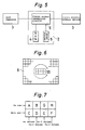
- all pixels on the screen are grouped into groups each of which is composed of four pixels contiguous to each other as shown by arrow II on the display panel composed of a plurality of pixels arranged in the form of matrix on it as shown schematically in the plan view of Figure 1.
- numeral 1 indicates turning a pixel on and numeral 0 indicates turning a pixel off.
- Figure 2 is a plan view schematically showing a magnification of one group of pixels shown by arrow II in the display panel.
- the pixel arrangement is set so that in Figure 2 the two upper pixels A and B are in an even-numbered row, the two lower pixels C and D are in an odd-numbered row, the two left pixels A and C are in an even-numbered column, and the two right pixels B and D are in an odd-numbered column.
- Figure 3 is a schematic diagram showing a gradation rule of each of pixels A to D within one group in case of displaying the 6/8 gradation level all over the screen of the display panel 1 according to the gradation rule.
- brightness level as a whole of a unit image area of one group composed of pixels A to D is as shown in Figure 4.
- the brightness level is always 3/4. Accordingly, the 6/8 brightness level is displayed on the average during one integration time period consisting of eight frame time periods and brightness level of the group does not vary as a whole of the unit image area, so flicker is reduced.
- a capacitive display device as a liquid crystal display device shows a phenomenon that brightness of the pixel turned on at that time varies according to the number of pixels turned on out of the pixels arranged in one row (common line) on the screen of the display panel 1
- difference between the number of pixels turned on in a subgroup of pixels A and B in the upper even-numbered row out of the pixels A to D within one group and the number of pixels turned on in a subgroup of pixels C and D in the lower odd-numbered row causes such deterioration of quality of the display that brightness of the pixels vary for each frame time period and the bright points seem to be vibrating.
- An object of the present invention is to provide a display driving method which makes it possible to display a high quality image with no noticeable flicker and no delicate shades of brightness among pixels of the same gradation level even in case of such a capacitive display device as a liquid crystal display device.
- the invention provides a display driving method for driving a display device having a plurality of scanning lines which makes a gradationally toned display with several brightness levels by setting a plurality of frame time periods, during which each of pixels on its screen is controlled for displaying an image, as one integration time period and by turning on pixels for a number of specified frame time periods corresponding to display data of the image within the integration time period, the display driving method making a gradationally toned display by, grouping all pixels of the display device into groups each of which is composed of a plurality of pixels contiguous to each other, selecting the number of pixels to be turned on for each of the frame time periods within one integration time period corresponding to the specified gradation data of each group, so that the number of pixels to be turned on for one frame time period may be equal between subgroups in the scanning lines within the same group, and setting the frame time period during which the number of pixels to be turned on is kept constant to a period shorter than a predetermined period.
- the invention provides a display driving method which makes a gradationally toned display by using multiple gradation data for each frame time period on the basis of a plurality of gradation data which are apart by nearly equal level from the specified gradation data in the directions opposite to each other.
- the invention provides a display device driving method which makes a gradationally toned display by turning on a number of pixels corresponding to the specified gradation data for each frame time period.
- the invention provides a display driving method in which each of the pixels to be turned on is selected from pixels in different positions within the group for each frame time period.
- the invention provides a display driving method in which difference between the plural gradation data is selected so as to be the minimum unit of gradation data.
- the invention provides a display driving method in which a period of variation among the plural gradation data is selected so as to be the same period as the frame time period.
- all pixels of a display device are grouped into plural groups each of which is composed of plural pixels contiguous to each other, and the number of pixels to be turned on for each frame time period within one integration time period is selected corresponding to the specified gradation data, so that the number of pixels to be turned on for one frame time period may be equal between subgroups in the scanning lines within the same group.
- the frame time period during which the number of pixels to be turned on is kept constant is selected so as to be shorter than a predetermined period, namely, the minimum period for which a human being feels flicker.
- selecting the number of pixels to be turned on out of plural pixels contiguous to each other to form one group for each frame time period corresponding to its display data reduces variation of brightness as a whole of one group of plural pixels and makes it possible to obtain a gradationally toned display without noticeable flicker.
- Figure 5 is a block diagram showing roughly a liquid crystal display device driving method to which a driving method of an embodiment of the invention is applied.
- a controller 2 which is a circuit to control driving of a liquid crystal display device 3, consists of a random access memory 4 (hereinafter referred as to RAM) which stores display data including their gradation data, a switch group 5 which sets gradation rules of a frame thinning out system, and a timing signal generating circuit 6 which generates timing signals necessary for making the liquid crystal display device 3 display an image.
- a host computer 7 is in charge of controlling the timing signal generating circuit 6.
- Figure 6 is a plan view schematically showing a display panel 8 of the liquid crystal display device 3 in which a plurality of pixels are arranged in the form of matrix
- Figure 7 is a plan view schematically showing a magnification of one group of pixels shown by arrow VII in the display panel 8.
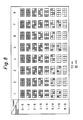
- Figure 8 is a schematic diagram showing gradation rules applied to the liquid crystal display device driving method in case of displaying a uniform gradation throughout the screen (a display in a uniform gradation all over the screen of the display panel 8), and
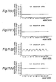
- Figure 9 is a set of schematic diagrams showing variation of brightness in a gradational display controlled by the method. Referring to Figure 8 and 9, operation of the liquid crystal display device driving method is described as follows.
- a gradationally toned display with 9 levels of the 0/8 (0 level), 1/8, 2/8, 3/8, 4/8, 5/8, 6/8, 7/8, and 8/8 (1 level) gradation levels is performed by setting eight frame time periods as one integration time period, a case is described that a unit image area with the 0/8, 1/8, 2/8, 3/8, 4/8, 5/8, 6/8, 7/8, or 8/8 gradation level in brightness is displayed with a group of pixels A, B, C, D, E, F, G and H shown in Figure 7.
- all pixels on the display panel 8 are grouped into a plurality of groups each of which is composed of the pixels shown in Figure 7 so that in a group of pixels shown in Figure 7 the upper pixels A, B, G, and H may be in the (2m)th row on the screen, the lower pixels C, D, E, and F may be in the (2m+1)th row on the screen, the pixels A and C in the leftmost column may be in the (4n)th column, the pixels B and D in the 2nd column from the left may be in the (4n+1)th column on the screen, the pixels G and E in the 3rd column from the left may be in the (4n+2)th column on the screen, and the pixels H and F in the rightmost column may be in the (4n+3)th column on the screen (where m and n are respectively integers which are equal to or greater than 0 and independent from each other).
- the gradation rules shown in Figure 8 are applied to the pixels A to H. Namely, in this case the gradation rules applied to the pixels A to D are exactly the same as the gradation rules applied to the pixels A to D in case of the proposed example shown in Table 1.
- the on/off state of the lower pixels E and F is set to the same as the on/off state of the upper pixels A and B in each frame, and the on/off state of the upper pixels G and H is set to the same as the on/off state of the lower pixels C and D.
- the off (no lighting) state is always selected for all of the eight pixels A to H throughout all of the eight frame time periods, and after this the same cycle is repeated.
- the on (lighting) state is selected for the two pixels A and E in the first frame out of the eight frames
- the off state is selected for all of the eight pixels A to H in the second frame
- the on state is selected for the two pixels B and F in the third frame
- the off state is selected again for all of the eight pixels A to H in the fourth frame
- the on state is selected for the two pixels C and G in the 5th frame
- the off state is selected again for all of the eight pixels A to H in the 6th frame
- the on state is selected for the two pixels D and H in the 7th frame
- the off state is selected for all of the eight pixels A to H in the 8th frame; and after this the same cycle is repeated.
- each of the pixels A to H is turned on equally once (in one frame) during the eight frame time periods.
- the on state is selected for the pixels A and E in the first frame, for the pixels B and F in the second frame, for the pixels C and G in the third frame, for the pixels D and H in the 4th frame, and the pixel control rules in the first to fourth frames are repeated in the 5th to 8th frames; and after this the same cycle is repeated.
- the pixel control rules in the first to fourth frames are repeated in the 5th to 8th frames; and after this the same cycle is repeated.
- two pixels are turned on in all frames and each of the pixels A to H is turned on equally twice during the eight frame time periods.
- the on state is selected for the pixels A and E in the first frame, for the pixels B, C, F, and G in the second frame, for the pixels C and G in the third frame, for the pixels A, D, E, and H in the 4th frame, for the pixels D and H in the 5th frame, for the pixels B, C, F, and G in the 6th frame, for the pixels B and F in the 7th frame, and for the pixels A, D, E, and H in the 8th frame; and after this the same cycle is repeated.
- a frame in which two pixels are turned on and another frame in which four pixels are turned on are alternately displayed, and each of the pixels A to H is turned on equally three times during the eight frame time periods.
- the on state is selected for the pixels A, C, E, and G in the first frame and for the pixels B, D, F, and H in the second frame and the gradation rules in the first and second frames are repeatedly applied to the 3rd to 8th frames; and after this the same cycle is repeated.
- the 4/8 gradation level four pixels are turned on in all of the eight frames and each of the pixels A to H is turned on equally 4 times during the 8 frames.
- the on state is selected for the pixels B, C, D, F, G, and H in the first frame, for the pixels A, C, D, E, G, and H in the second frame, for the pixels A, B, D, E, F, and H in the third frame, for the pixels A, B, C, E, F, and G in the 4th frame, and the gradation rules in the first to fourth frames are repeatedly applied to the 5th to 8th frames; and after this the same cycle is repeated.
- the 6/8 gradation level six pixels are turned on in all the frames and each of the pixels A to H is turned on equally 6 times during the eight frame time periods.
- the on state is selected for the pixels B, C, D, F, G, and H in the first frame, for all of the pixels A to H in the second frame, for the pixels A, C, D, E, G, and H in the third frame, for all of the pixels A to H in the fourth frame, for the pixels A, B, D, E, F, and H in the 5th frame, for all of the pixels A to H in the 6th frame, for the pixels A, B, C, E, F, and G in the 7th frame, and for all of the pixels A to H in the 8th frame; and after this the same cycle is repeated.
- a frame in which six pixels are turned on and another frame in which eight pixels are turned on are alternately displayed and each of the pixels A to H is turned on equally 7 times during the eight frame time periods.
- the on state is always selected for all of the eight pixels A to H during the eight frame time periods, and after this the same cycle is repeated.
- the controller 2 drives the eight pixels A to H forming one group in the display panel 8 of the liquid crystal display device 3.
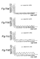
- brightness levels as a whole of one group composed of the 8 pixels A to H in the display panel 8 are as shown in Figures 9 (a), (b), (c), (d), (e), (f), (g), and (h).
- the brightness level is always 0 as shown in Figure 9 (a). Accordingly, the average brightness level is also 0 during one integration time period consisting of 8 frame time periods. In this case, since the brightness level does not vary, no flicker occurs.
- the on/off state of the pixels A and B in the upper row out of the pixels A to H of one group is the same as the on/off state of the pixels E and F in the lower row and the on/off state of the pixels C and D in the lower row is the same as the on/off state of the pixels G and H in the upper row
- the number of pixels turned on out of the pixels A, B, G, and H in the upper row and the number of pixels turned on out of the pixels C, D, E, and F in the lower row within one group are always equal to each other. Accordingly, in case that the same brightness level of display is displayed all over the screen, the number of pixels turned on out of the pixels arranged in one scanning line in a frame is always the same as that in any other frame. As a result, brightness of pixels turned on does not happen to vary in each frame and any delicate shades of brightness do not occur among pixels.
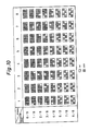
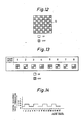
- Figure 10 is a schematic diagram showing gradation rules for displaying a checker pattern as shown in Figure 12 on the basis of the gradation rules shown in Figure 8, and Figure 11 is a set of schematic diagrams showing variation of brightness level in a gradational display obtained by the gradation rules in Figure 10.
- a pixel to be turned on out of pixels on the display panel 8 is indicated as a blank box, and a pixel to be turned off is indicated as a hatched box.
- the pixel in the upper left hand corner of the screen and pixels alternately disposed following it are turned on. Accordingly, the gradation rules shown in Figure 10 are equivalent to those according to which the pixels B, C, E, and H out of the pixels A to H controlled according to the gradation rules shown in Figure 8 are turned off throughout all frame time periods.
- the pixels F and G to be set in the same on/off state as the pixels B and C are not changed to be turned off among the pixels E, F, G, and H in order to display a checker pattern, even in case that the pixels B and C to be originally turned on are changed to be turned off in order to display a checker pattern among the pixels A, B, C, and D. Namely, it is the pixels E and H that are changed to be turned off among the pixels E, F, G, and H in order to display a checker pattern in spite of being originally turned on.
- the pixels E and H are changed to be turned off in order to display a checker pattern in spite of being originally turned on, among the pixels A, B, C, and D the pixels A and D to be set in the same on/off state as the pixels E and H are not changed to be turned off in order to display a checker pattern. Accordingly, the number of pixels turned on in each frame according to the gradation rules in case of displaying a checker pattern is reduced to one half as compared with that according to the gradation rules shown in Figure 8, but the corresponding relation between the number of pixels turned on and the gradation levels is kept equal in both cases.
- the on/off state of the pixels is the same as that in Figure 8, but in case of displaying the 1/8 gradation level, the pixel A is turned on in the 1st frame, all the pixels are turned off in the 2nd frame, the pixel F is turned on in the 3rd frame, all the pixels are turned off in the 4th frame, the pixel G is turned on in the 5th frame, all the pixels are turned off in the 6th frame, the pixel D is turned on in the 7th frame, and all the pixels are turned off in the 8th frame.
- a frame in which one pixel is turned on and another frame in which all of the 8 pixels A to H are turned off are alternately displayed.
- the on state is selected for the pixel A in the 1st frame, for the pixel F in the 2nd frame, for the pixel G in the 3rd frame, for the pixel D in the 4th frame, and the same gradation rules as the 1st to 4th frames are applied to the 5th to 8th frames. Namely, in displaying the 2/8 gradation level, one pixel is turned on in all frames.
- the on state is selected for the pixel A in the 1st frame, for the pixels F and G in the 2nd frame, for the pixel G in the 3rd frame, for the pixels A and D in the 4th frame, for the pixel D in the 5th frame, for the pixels F and G in the 6th frame, for the pixel F in the 7th frame, and for the pixels A and D in the 8th frame.
- a frame in which one pixel is turned on and another frame in which two pixels are turned on are alternately displayed.
- the on state is selected for the pixels A and G in the 1st frame, for the pixels D and F in the 2nd frame, and after this the same cycle is repeated. Namely, in displaying the 4/8 gradation level, two pixels are turned on in all frames.
- the on state is selected for the pixels D, F, and G in the 1st frame, for the pixels A, D, and G in the 2nd frame, for the pixels A, D, and F in the 3rd frame, for the pixels A, F, and G in the 4th frame, and the same gradation rules as the 1st to 4th frames are applied to the 5th to 8th frames. Namely, in displaying the 6/8 gradation level, three pixels are turned on in all frames.
- the on state is selected for the pixels D, F, and G in the 1st frame, for the pixels A, D, F, and G in the 2nd frame, for the pixels A, D, and G in the 3rd frame, for the pixels A, D, F, and G in the 4th frame, for the pixels A, D, and F in the 5th frame, for the pixels A, D, F, and G in the 6th frame, for the pixels A, F, and G in the 7th frame, and for the pixels A, D, F, and G in the 8th frame.
- a frame in which three pixels are turned on and another frame in which four pixels are turned on are alternately displayed.
- the on state is selected for the pixels A, D, F, and G in all frames. Namely, in displaying the 8/8 gradation level, four pixels are turned on in all frames.
- brightness levels as a whole of one group composed of the 8 pixels A to H in the display panel 8 are as shown in Figure 11 (a), (b), (d), (c), (e), (f), (g), and (h).
- Figure 3 is a schematic diagram showing the gradation rule for the 6/8 gradation level in Table 1.
- the gradation rule for displaying a checker pattern as shown in Figure 12 is indicated by a schematic diagram shown in Figure 13.
- the schematic diagram shown in Figure 13 is equalent to the case of turning off the pixels B and C in all frames in the schematic diagram shown in Figure 3. Accordingly, brightness as a whole of the unit image area of one group composed of the four pixels A to D is as shown in Figure 14.
- the one pixel D is turned on in the first frame and the brightness level is 1/4
- the two pixels A and D are turned on in the second frame and the brightness level is 2/4
- the two pixels A and D are turned on in the third frame also and the brightness level is 2/4
- the one pixel A is turned on in the 4th frame and the brightness level is 1/4
- the gradation rules in the first to fourth frames are repeatedly applied to the fifth to eighth frames.
- the brightness level is 2/4 in consecutive two frames and is 1/4 in the following consecutive two frames, and this cycle is repeated.
- a frequency of alternating the 1/4 and 2/4 brightness levels is one fourth of the frame frequency, and is less than the frequency in case of the same 6/8 brightness level in the above-mentioned embodiment.
- the frame frequency is 80 Hz or so
- the frequency of alternating becomes 20 Hz or so, and as a result flicker comes out to be very noticeable and causes deterioration of quality of the display.
- the frequency of alternating variation of brightness level is at least a half or so of the frame frequency, so flicker is not so much noticeable as mentioned above.
Abstract
Description
- The present invention relates to a method for driving such display devices as a liquid crystal display device, thin film EL display device, and the like.
- For a liquid crystal display device and the like, a frame thinning out system is well-known as one of driving methods for enabling such a display panel to display a gradationally toned image with several brightness levels on its screen.
- The frame thinning out system turns on pixels only in a number of frames corresponding to a level of brightness to be displayed out of all frames within an integration time period consisting of a plurality of frame time periods so as to visually obtain a medium level of brightness in each integration time period.
- The applicant of the invention has already proposed a driving method to reduce flicker on the screen by grouping all pixels of the display device into groups each of which is composed of a plurality of pixels contiguous to each other and limiting the total number of pixels to be turned on for each frame time period within the same group according to its display data as a display driving method improving the conventional frame thinning out system.
- Table 1 shows gradation rules (rules of turning pixels on or off for which frame time period) in case of making a gradational display by setting eight frame time periods as one integration time period by means of this driving method. In this case, all pixels on the screen are grouped into groups each of which is composed of four pixels contiguous to each other as shown by arrow II on the display panel composed of a plurality of pixels arranged in the form of matrix on it as shown schematically in the plan view of Figure 1.
Table 1 Frame 1 2 3 4 5 6 7 8 Gradation level Pixel 0/8 A 0 0 0 0 0 0 0 0 B 0 0 0 0 0 0 0 0 C 0 0 0 0 0 0 0 0 D 0 0 0 0 0 0 0 0 1/8 A 1 0 0 0 0 0 0 0 B 0 0 1 0 0 0 0 0 C 0 0 0 0 1 0 0 0 D 0 0 0 0 0 0 1 0 2/8 A 1 0 0 0 1 0 0 0 B 0 1 0 0 0 1 0 0 C 0 0 1 0 0 0 1 0 D 0 0 0 1 0 0 0 1 3/8 A 1 0 0 1 0 0 0 1 B 0 1 0 0 0 1 1 0 C 0 1 1 0 0 1 0 0 D 0 0 0 1 1 0 0 1 4/8 A 1 0 1 0 1 0 1 0 B 0 1 0 1 0 1 0 1 C 1 0 1 0 1 0 1 0 D 0 1 0 1 0 1 0 1 6/8 A 0 1 1 1 0 1 1 1 B 1 0 1 1 1 0 1 1 C 1 1 0 1 1 1 0 1 D 1 1 1 0 1 1 1 0 7/8 A 0 1 1 1 1 1 1 1 B 1 1 0 1 1 1 1 1 C 1 1 1 1 0 1 1 1 D 1 1 1 1 1 1 0 1 8/8 A 1 1 1 1 1 1 1 1 B 1 1 1 1 1 1 1 1 C 1 1 1 1 1 1 1 1 D 1 1 1 1 1 1 1 1 - In Table 1,
numeral 1 indicates turning a pixel on andnumeral 0 indicates turning a pixel off. - Figure 2 is a plan view schematically showing a magnification of one group of pixels shown by arrow II in the display panel. In the grouping, when setting the pixel in the upper left hand corner of the screen of the
display panel 1 as a pixel in the 0th row and 0th column, the pixel arrangement is set so that in Figure 2 the two upper pixels A and B are in an even-numbered row, the two lower pixels C and D are in an odd-numbered row, the two left pixels A and C are in an even-numbered column, and the two right pixels B and D are in an odd-numbered column. - Figure 3 is a schematic diagram showing a gradation rule of each of pixels A to D within one group in case of displaying the 6/8 gradation level all over the screen of the
display panel 1 according to the gradation rule. - As known from Figure 3, in case of displaying the 6/8 gradation level, three pixels B, C and D are turned on (the pixels A is turned off) for the first frame time period, three pixels A, C and D are turned on (the pixel B is off) for the second frame time period, three pixels A, B and D are turned on (the pixel C is off) for the third frame time period, and three pixels A, B and C are turned on for the fourth frame time period. The rule for the first to fourth frame time periods is also applied to the fifth to eighth frame time periods, and after this the cycle is repeated which has the eight frame time periods as an integration time period. Namely, in case of displaying the 6/8 gradation level, three pixels are always turned on for each frame time period and each of pixels A to D are turned on equally six times for eight frame time periods.
- In this case brightness level as a whole of a unit image area of one group composed of pixels A to D is as shown in Figure 4.
- Namely, since three pixels are turned on throughout all frame time periods, the brightness level is always 3/4. Accordingly, the 6/8 brightness level is displayed on the average during one integration time period consisting of eight frame time periods and brightness level of the group does not vary as a whole of the unit image area, so flicker is reduced.
- In the above-mentioned driving method previously proposed, however, as shown in Figure 3, in case of the 6/8 brightness level the number of pixels turned on in a subgroup of pixels A and B in the upper even-numbered row out of the pixels A to D within one group for each frame time period is different from the number of pixels turned on in a subgroup of pixels C and D in the lower odd-numbered row. As a result, there has been a problem that quality of the display is deteriorated depending on a viewing angle in case that the above-mentioned driving method is applied to such a capacitive display device as a liquid crystal display device.
- Namely, since such a capacitive display device as a liquid crystal display device shows a phenomenon that brightness of the pixel turned on at that time varies according to the number of pixels turned on out of the pixels arranged in one row (common line) on the screen of the
display panel 1, difference between the number of pixels turned on in a subgroup of pixels A and B in the upper even-numbered row out of the pixels A to D within one group and the number of pixels turned on in a subgroup of pixels C and D in the lower odd-numbered row causes such deterioration of quality of the display that brightness of the pixels vary for each frame time period and the bright points seem to be vibrating. - This problem occurs also in case of displaying the other gradation levels.
- An object of the present invention is to provide a display driving method which makes it possible to display a high quality image with no noticeable flicker and no delicate shades of brightness among pixels of the same gradation level even in case of such a capacitive display device as a liquid crystal display device.
- The invention provides a display driving method for driving a display device having a plurality of scanning lines which makes a gradationally toned display with several brightness levels by setting a plurality of frame time periods, during which each of pixels on its screen is controlled for displaying an image, as one integration time period and by turning on pixels for a number of specified frame time periods corresponding to display data of the image within the integration time period, the display driving method making a gradationally toned display by,
grouping all pixels of the display device into groups each of which is composed of a plurality of pixels contiguous to each other,
selecting the number of pixels to be turned on for each of the frame time periods within one integration time period corresponding to the specified gradation data of each group, so that the number of pixels to be turned on for one frame time period may be equal between subgroups in the scanning lines within the same group, and
setting the frame time period during which the number of pixels to be turned on is kept constant to a period shorter than a predetermined period. - And the invention provides a display driving method which makes a gradationally toned display by using multiple gradation data for each frame time period on the basis of a plurality of gradation data which are apart by nearly equal level from the specified gradation data in the directions opposite to each other.
- Further, the invention provides a display device driving method which makes a gradationally toned display by turning on a number of pixels corresponding to the specified gradation data for each frame time period.
- Still further, the invention provides a display driving method in which each of the pixels to be turned on is selected from pixels in different positions within the group for each frame time period.
- And furthermore, the invention provides a display driving method in which difference between the plural gradation data is selected so as to be the minimum unit of gradation data.
- Still furthermore, the invention provides a display driving method in which a period of variation among the plural gradation data is selected so as to be the same period as the frame time period.
- According to the invention, all pixels of a display device are grouped into plural groups each of which is composed of plural pixels contiguous to each other, and the number of pixels to be turned on for each frame time period within one integration time period is selected corresponding to the specified gradation data, so that the number of pixels to be turned on for one frame time period may be equal between subgroups in the scanning lines within the same group. And the frame time period during which the number of pixels to be turned on is kept constant is selected so as to be shorter than a predetermined period, namely, the minimum period for which a human being feels flicker.
- Accordingly, in case of viewing a plurality of pixels all over one group as a unit image area, a high quality gradational display without noticeable flicker can be obtained. And since no delicate shades of brightness occur among pixels to display the same gradation level, quality of the display is improved.
- As mentioned above, according to a display device driving method by the invention, selecting the number of pixels to be turned on out of plural pixels contiguous to each other to form one group for each frame time period corresponding to its display data reduces variation of brightness as a whole of one group of plural pixels and makes it possible to obtain a gradationally toned display without noticeable flicker.
- Since the number of pixels to be turned on for each frame time period is equal to each other among the subgroups respectively arranged in the scanning line within the same group, no delicate shades of brightens occur among pixels to display the same gradation level even in case of applying this driving method to such a capacitive display device as a liquid crystal display device; and as a result, quality of the display is improved so much.
- These objects, the other objects, features, and merits of the present invention will be clarified more expressly by the following detailed descriptions and drawings.
- Figure 1 is a plan view of the display panel schematically shown to explain grouping of the pixels in a driving method previously proposed as an example,
- Figure 2 is a plan view schematically showing a magnification of one group of pixels of the display panel,
- Figure 3 is a schematic diagram showing a gradation rule for displaying the 6/8 gradation level in the driving method proposed as an example,
- Figure 4 is a schematic diagram showing variation of brightness in one group of pixels controlled on the basis of the gradation rule,
- Figure 5 is a block diagram to show roughly configuration of a liquid crystal display device driving method to which a driving method of an embodiment of the invention is applied,
- Figure 6 is a plan view schematically showing the display panel of the liquid crystal display device,
- Figure 7 is a plan view schematically showing a magnification of one group of pixels of the display panel,
- Figure 8 is a schematic diagram showing gradation rules applied to the liquid crystal display device driving method,
- Figure 9 is a set of schematic diagrams showing variation of brightness in one group of pixels controlled on the basis of the gradation rules,
- Figure 10 is a schematic diagram showing gradation rules in case of display a checker pattern on the basis of the above-mentioned gradation rules,
- Figure 11 is a set of schematic diagrams showing variation of brightness in one group of pixels controlled on the basis of the gradation rules,
- Figure 12 is a plan view schematically showing a display screen of the checker pattern,
- Figure 13 is a schematic diagram showing a gradation rule for the 6/8 gradation level in case of displaying a checker pattern on the basis of the gradation rule in the driving method previously proposed as an example, and
- Figure 14 is a schematic diagram showing variation of brightness in one group of pixels controlled on the basis of this gradation rule.
- Referring to the drawings, a preferred embodiment of the present invention is described in details below.
- Figure 5 is a block diagram showing roughly a liquid crystal display device driving method to which a driving method of an embodiment of the invention is applied.
- In Figure 5, a
controller 2, which is a circuit to control driving of a liquidcrystal display device 3, consists of a random access memory 4 (hereinafter referred as to RAM) which stores display data including their gradation data, aswitch group 5 which sets gradation rules of a frame thinning out system, and a timingsignal generating circuit 6 which generates timing signals necessary for making the liquidcrystal display device 3 display an image. Ahost computer 7 is in charge of controlling the timingsignal generating circuit 6. - Figure 6 is a plan view schematically showing a
display panel 8 of the liquidcrystal display device 3 in which a plurality of pixels are arranged in the form of matrix, and Figure 7 is a plan view schematically showing a magnification of one group of pixels shown by arrow VII in thedisplay panel 8. - Figure 8 is a schematic diagram showing gradation rules applied to the liquid crystal display device driving method in case of displaying a uniform gradation throughout the screen (a display in a uniform gradation all over the screen of the display panel 8), and Figure 9 is a set of schematic diagrams showing variation of brightness in a gradational display controlled by the method. Referring to Figure 8 and 9, operation of the liquid crystal display device driving method is described as follows.
- Assuming that a gradationally toned display with 9 levels of the 0/8 (0 level), 1/8, 2/8, 3/8, 4/8, 5/8, 6/8, 7/8, and 8/8 (1 level) gradation levels is performed by setting eight frame time periods as one integration time period, a case is described that a unit image area with the 0/8, 1/8, 2/8, 3/8, 4/8, 5/8, 6/8, 7/8, or 8/8 gradation level in brightness is displayed with a group of pixels A, B, C, D, E, F, G and H shown in Figure 7.
- When setting the pixel in the upper left hand corner of the screen of the
display panel 8 shown in Figure 6 as a pixel in the 0th row and 0th column, all pixels on thedisplay panel 8 are grouped into a plurality of groups each of which is composed of the pixels shown in Figure 7 so that in a group of pixels shown in Figure 7 the upper pixels A, B, G, and H may be in the (2m)th row on the screen, the lower pixels C, D, E, and F may be in the (2m+1)th row on the screen, the pixels A and C in the leftmost column may be in the (4n)th column, the pixels B and D in the 2nd column from the left may be in the (4n+1)th column on the screen, the pixels G and E in the 3rd column from the left may be in the (4n+2)th column on the screen, and the pixels H and F in the rightmost column may be in the (4n+3)th column on the screen (where m and n are respectively integers which are equal to or greater than 0 and independent from each other). - In the
switch group 5 shown in Figure 5, the gradation rules shown in Figure 8 are applied to the pixels A to H. Namely, in this case the gradation rules applied to the pixels A to D are exactly the same as the gradation rules applied to the pixels A to D in case of the proposed example shown in Table 1. When setting the driving data of turning on or off the pixels A, B, C, D, E, F, G, and H respectively as a, b, c, d, e, f, g, and h, the gradation rules shown in Figure 8 sets a=e, b=f, c=g, and d=h. Namely, for the pixels in Figure 7, the on/off state of the lower pixels E and F is set to the same as the on/off state of the upper pixels A and B in each frame, and the on/off state of the upper pixels G and H is set to the same as the on/off state of the lower pixels C and D. - In case of displaying the 0/8 gradation level, concretely, the off (no lighting) state is always selected for all of the eight pixels A to H throughout all of the eight frame time periods, and after this the same cycle is repeated.
- In case of displaying the 1/8 gradation level, the on (lighting) state is selected for the two pixels A and E in the first frame out of the eight frames, the off state is selected for all of the eight pixels A to H in the second frame, the on state is selected for the two pixels B and F in the third frame, the off state is selected again for all of the eight pixels A to H in the fourth frame, the on state is selected for the two pixels C and G in the 5th frame, the off state is selected again for all of the eight pixels A to H in the 6th frame, the on state is selected for the two pixels D and H in the 7th frame, and the off state is selected for all of the eight pixels A to H in the 8th frame; and after this the same cycle is repeated. Namely, in displaying the 1/8 gradation level, a frame in which two pixels are turned on and another frame in which all of the eight pixels are turned off are alternately displayed. In this case, each of the pixels A to H is turned on equally once (in one frame) during the eight frame time periods.
- In case of displaying the 2/8 gradation level, the on state is selected for the pixels A and E in the first frame, for the pixels B and F in the second frame, for the pixels C and G in the third frame, for the pixels D and H in the 4th frame, and the pixel control rules in the first to fourth frames are repeated in the 5th to 8th frames; and after this the same cycle is repeated. Namely, in displaying the 2/8 gradation level, two pixels are turned on in all frames and each of the pixels A to H is turned on equally twice during the eight frame time periods.
- In case of displaying the 3/8 gradation level, the on state is selected for the pixels A and E in the first frame, for the pixels B, C, F, and G in the second frame, for the pixels C and G in the third frame, for the pixels A, D, E, and H in the 4th frame, for the pixels D and H in the 5th frame, for the pixels B, C, F, and G in the 6th frame, for the pixels B and F in the 7th frame, and for the pixels A, D, E, and H in the 8th frame; and after this the same cycle is repeated. Namely, in displaying the 3/8 gradation level, a frame in which two pixels are turned on and another frame in which four pixels are turned on are alternately displayed, and each of the pixels A to H is turned on equally three times during the eight frame time periods.
- In case of displaying the 4/8 gradation level, the on state is selected for the pixels A, C, E, and G in the first frame and for the pixels B, D, F, and H in the second frame and the gradation rules in the first and second frames are repeatedly applied to the 3rd to 8th frames; and after this the same cycle is repeated. Namely, in displaying the 4/8 gradation level, four pixels are turned on in all of the eight frames and each of the pixels A to H is turned on equally 4 times during the 8 frames.
- In case of displaying the 6/8 gradation level, the on state is selected for the pixels B, C, D, F, G, and H in the first frame, for the pixels A, C, D, E, G, and H in the second frame, for the pixels A, B, D, E, F, and H in the third frame, for the pixels A, B, C, E, F, and G in the 4th frame, and the gradation rules in the first to fourth frames are repeatedly applied to the 5th to 8th frames; and after this the same cycle is repeated. Namely, in displaying the 6/8 gradation level, six pixels are turned on in all the frames and each of the pixels A to H is turned on equally 6 times during the eight frame time periods.
- In case of displaying the 7/8 gradation level, the on state is selected for the pixels B, C, D, F, G, and H in the first frame, for all of the pixels A to H in the second frame, for the pixels A, C, D, E, G, and H in the third frame, for all of the pixels A to H in the fourth frame, for the pixels A, B, D, E, F, and H in the 5th frame, for all of the pixels A to H in the 6th frame, for the pixels A, B, C, E, F, and G in the 7th frame, and for all of the pixels A to H in the 8th frame; and after this the same cycle is repeated. Namely, in displaying the 7/8 gradation level, a frame in which six pixels are turned on and another frame in which eight pixels are turned on are alternately displayed and each of the pixels A to H is turned on equally 7 times during the eight frame time periods.
- In case of displaying the 8/8 gradation level, the on state is always selected for all of the eight pixels A to H during the eight frame time periods, and after this the same cycle is repeated.
- According to these gradation rules, the
controller 2 drives the eight pixels A to H forming one group in thedisplay panel 8 of the liquidcrystal display device 3. In these cases, brightness levels as a whole of one group composed of the 8 pixels A to H in thedisplay panel 8 are as shown in Figures 9 (a), (b), (c), (d), (e), (f), (g), and (h). - That is to say, in case of displaying the 0/8 gradation level, since all of the 8 pixels A to H are turned off throughout all frame time periods, the brightness level is always 0 as shown in Figure 9 (a). Accordingly, the average brightness level is also 0 during one integration time period consisting of 8 frame time periods. In this case, since the brightness level does not vary, no flicker occurs.
- In case of displaying the 1/8 gradation level, as shown in Figure 9 (b), since two pixels are turned on in the first frame the brightness level is 2/8 and since all of the 8 pixels are turned off in the second frame the brightness level becomes 0, and this cycle is repeated. As a result, the 1/8 brightness level is displayed on the average during one integration time period consisting of 8 frame time periods. And since a frequency of alternating the 2/8 and 0 brightness levels is a half of the frame frequency and (quadruple) greater than the frequency having 8 frame periods as one integration period, flicker is reduced so much.
- In case of displaying the 2/8 gradation level, as shown in Figure 9 (c), since two pixels are always turned on throughout all frame time periods, the brightness level is always 2/8. Accordingly, the average brightness level is also 2/8 during one integration time period consisting of 8 frame time periods. In this case, since the brightness level does not vary, no flicker occurs.
- In case of displaying the 3/8 gradation level, as shown in Figure 9 (d), since two pixels are turned on in the first frame the brightness level is 2/8 and since four pixels are turned on in the second frame the brightness level becomes 4/8, and this cycle is repeated. As a result, the 3/8 brightness level is displayed on the average during one integration time period consisting of 8 frame time periods. And since a frequency of alternating the 2/8 and 4/8 brightness levels is a half of the frame frequency and (quadruple) greater than the frequency having 8 frame periods as one integration period, flicker is reduced so much.
- In case of displaying the 4/8 gradation level, as shown in Figure 9 (e), since four pixels are always turned on throughout all frame time periods, the brightness level is always 4/8. Accordingly, the average brightness level is also 4/8 during one integration time period consisting of 8 frame time periods. In this case also, since the brightness level does not vary, no flicker occurs.
- In case of displaying the 6/8 gradation level also, as shown in Figure 9 (f), since six pixels are always turned on throughout all frame time periods, the brightness level is always 6/8. In this case also, since the brightness level does not vary, no flicker occurs.
- In case of displaying the 7/8 gradation level, as shown in Figure 9 (g), since six pixels are turned on in the first frame the brightness level is 6/8 and since all of the 8 pixels are turned on in the second frame the brightness level becomes 8/8, and this cycle is repeated. As a result, the 7/8 brightness level is displayed on the average during one integration time period consisting of 8 frame time periods. And since a frequency of alternating the 6/8 and 8/8 brightness levels is a half of the frame frequency and greater than the frequency having 8 frame periods as one integration time period, flicker is reduced so much.
- And in case of displaying the 8/8 gradation level, as shown in Figure 9 (h), since all of the 8 pixels are always turned on throughout all frame time periods, the brightness level is always 8/8. Accordingly the average brightness level is also 8/8 during one integration time period consisting of 8 frame time periods. In this case also, since the brightness level does not vary, no flicker occurs.
- As mentioned above, since the on/off state of the pixels A and B in the upper row out of the pixels A to H of one group is the same as the on/off state of the pixels E and F in the lower row and the on/off state of the pixels C and D in the lower row is the same as the on/off state of the pixels G and H in the upper row, the number of pixels turned on out of the pixels A, B, G, and H in the upper row and the number of pixels turned on out of the pixels C, D, E, and F in the lower row within one group are always equal to each other. Accordingly, in case that the same brightness level of display is displayed all over the screen, the number of pixels turned on out of the pixels arranged in one scanning line in a frame is always the same as that in any other frame. As a result, brightness of pixels turned on does not happen to vary in each frame and any delicate shades of brightness do not occur among pixels.
- Figure 10 is a schematic diagram showing gradation rules for displaying a checker pattern as shown in Figure 12 on the basis of the gradation rules shown in Figure 8, and Figure 11 is a set of schematic diagrams showing variation of brightness level in a gradational display obtained by the gradation rules in Figure 10.
- In Figure 12, a pixel to be turned on out of pixels on the
display panel 8 is indicated as a blank box, and a pixel to be turned off is indicated as a hatched box. The pixel in the upper left hand corner of the screen and pixels alternately disposed following it are turned on. Accordingly, the gradation rules shown in Figure 10 are equivalent to those according to which the pixels B, C, E, and H out of the pixels A to H controlled according to the gradation rules shown in Figure 8 are turned off throughout all frame time periods. - As mentioned above, since the gradation rules shown in Figure 8 are set so that the on/off state of the pixels A and B out of one group of pixels shown in Figure 7 may be equal to the on/off state of the pixels E and F and the on/off state of the pixels C and D may be equal to the on/off state of the pixels G and H, the pixels F and G to be set in the same on/off state as the pixels B and C are not changed to be turned off among the pixels E, F, G, and H in order to display a checker pattern, even in case that the pixels B and C to be originally turned on are changed to be turned off in order to display a checker pattern among the pixels A, B, C, and D. Namely, it is the pixels E and H that are changed to be turned off among the pixels E, F, G, and H in order to display a checker pattern in spite of being originally turned on.
- On the other hand, even in case that among the pixels E, F, G, and H the pixels E and H are changed to be turned off in order to display a checker pattern in spite of being originally turned on, among the pixels A, B, C, and D the pixels A and D to be set in the same on/off state as the pixels E and H are not changed to be turned off in order to display a checker pattern. Accordingly, the number of pixels turned on in each frame according to the gradation rules in case of displaying a checker pattern is reduced to one half as compared with that according to the gradation rules shown in Figure 8, but the corresponding relation between the number of pixels turned on and the gradation levels is kept equal in both cases.
- Namely, in Figure 10, in case of displaying the 0/8 gradation level, the on/off state of the pixels is the same as that in Figure 8, but in case of displaying the 1/8 gradation level, the pixel A is turned on in the 1st frame, all the pixels are turned off in the 2nd frame, the pixel F is turned on in the 3rd frame, all the pixels are turned off in the 4th frame, the pixel G is turned on in the 5th frame, all the pixels are turned off in the 6th frame, the pixel D is turned on in the 7th frame, and all the pixels are turned off in the 8th frame. Namely, in displaying the 1/8 gradation level, a frame in which one pixel is turned on and another frame in which all of the 8 pixels A to H are turned off are alternately displayed.
- In case of displaying the 2/8 gradation level, the on state is selected for the pixel A in the 1st frame, for the pixel F in the 2nd frame, for the pixel G in the 3rd frame, for the pixel D in the 4th frame, and the same gradation rules as the 1st to 4th frames are applied to the 5th to 8th frames. Namely, in displaying the 2/8 gradation level, one pixel is turned on in all frames.
- In case of displaying the 3/8 gradation level, the on state is selected for the pixel A in the 1st frame, for the pixels F and G in the 2nd frame, for the pixel G in the 3rd frame, for the pixels A and D in the 4th frame, for the pixel D in the 5th frame, for the pixels F and G in the 6th frame, for the pixel F in the 7th frame, and for the pixels A and D in the 8th frame. Namely, in displaying the 3/8 gradation level, a frame in which one pixel is turned on and another frame in which two pixels are turned on are alternately displayed.
- In case of displaying the 4/8 gradation level, the on state is selected for the pixels A and G in the 1st frame, for the pixels D and F in the 2nd frame, and after this the same cycle is repeated. Namely, in displaying the 4/8 gradation level, two pixels are turned on in all frames.
- In case of displaying the 6/8 gradation level, the on state is selected for the pixels D, F, and G in the 1st frame, for the pixels A, D, and G in the 2nd frame, for the pixels A, D, and F in the 3rd frame, for the pixels A, F, and G in the 4th frame, and the same gradation rules as the 1st to 4th frames are applied to the 5th to 8th frames. Namely, in displaying the 6/8 gradation level, three pixels are turned on in all frames.
- In case of displaying the 7/8 gradation level, the on state is selected for the pixels D, F, and G in the 1st frame, for the pixels A, D, F, and G in the 2nd frame, for the pixels A, D, and G in the 3rd frame, for the pixels A, D, F, and G in the 4th frame, for the pixels A, D, and F in the 5th frame, for the pixels A, D, F, and G in the 6th frame, for the pixels A, F, and G in the 7th frame, and for the pixels A, D, F, and G in the 8th frame. Namely, in displaying the 7/8 gradation level, a frame in which three pixels are turned on and another frame in which four pixels are turned on are alternately displayed.
- And in case of displaying the 8/8 gradation level, the on state is selected for the pixels A, D, F, and G in all frames. Namely, in displaying the 8/8 gradation level, four pixels are turned on in all frames.
- In these cases, brightness levels as a whole of one group composed of the 8 pixels A to H in the
display panel 8 are as shown in Figure 11 (a), (b), (d), (c), (e), (f), (g), and (h). - That is to say, in case of displaying the 0/8 gradation level, since all of the pixels A to H are turned off throughout all frame time periods, the brightness level is always 0 as shown in Figure 11 (a).
- In case of displaying the 1/8 gradation level, as shown in Figure 11 (b), since one pixel is turned on in the first frame the brightness level is 1/8 and since all of the 8 pixels are turned off in the 2nd frame the brightness level becomes 0, and this cycle is repeated. As a result, the 1/16 brightness level is displayed on the average during one integration time period consisting of 8 frame time periods. And since a frequency of alternating the 1/8 and 0 brightness levels is a half of the frame frequency and (quadruple) greater than the frequency having 8 frame periods as one integration period, flicker is reduced so much.
- In case of displaying the 2/8 gradation level, as shown in Figure 11 (c), since one pixel is always turned on throughout all frame time periods, the brightness level is always 1/8. Accordingly the average brightness level is also 1/8 during one integration time period consisting of 8 frame time periods. In this case, since the brightness level does not vary, no flicker occurs.
- In case of displaying the 3/8 gradation level, as shown in Figure 11 (d), since one pixel is turned on in the 1st frame the brightness level is 1/8 and since two pixels are turned on in the 2nd frame the brightness level becomes 2/8, and this cycle is repeated. As a result the 3/16 brightness level is displayed on the average during one integration time period consisting of 8 frame time periods. And since a frequency of alternating the 1/8 and 2/8 brightness levels is a half of the frame frequency and greater than the frequency having 8 frame periods as one integration period, flicker is reduced so much.
- In case of displaying the 4/8 gradation level, as shown in Figure 11 (e), since two pixels are always turned on throughout all frame time periods, the brightness level is always 2/8. Accordingly the average brightness level is also 2/8 during one integration time period consisting of 8 frame time periods. In this case also, since the brightness level does not vary, no flicker occurs.
- In case of displaying the 6/8 gradation level, as shown in Figure 11 (f), since three pixels are always turned on throughout all frame time periods, the brightness level is always 3/8. In this case also, since the brightness level does not vary, no flicker occurs.
- In case of displaying the 7/8 gradation level, as shown in Figure 11 (g), since three pixels are turned on in the 1st frame the brightness level is 3/8 and since four pixels are turned on in the 2nd frame the brightness level becomes 4/8, and this cycle is repeated. As a result the 7/16 brightness level is displayed on the average during one integration time period consisting of 8 frame time periods. And since a frequency of alternating the 3/8 and 4/8 brightness levels is a half of the frame frequency and greater than the frequency having 8 frame periods as one integration period, flicker is reduced so much.
- In case of displaying the 8/8 gradation level, as shown in Figure 11 (h), since four pixels are always turned on throughout all frame time periods, the brightness level is always 4/8. Accordingly the average brightness level is also 4/8 during one integration time period consisting of 8 frame time periods. In this case also, since the brightness level does not vary, no flicker occurs.
- By the way, in case of displaying the checker pattern shown in Figure 12 according to the gradation rules of the previously proposed example shown in Table 1, flicker is noticeable on the screen. This is described below taking the 6/8 gradation level of display as an example.
- Figure 3 is a schematic diagram showing the gradation rule for the 6/8 gradation level in Table 1. The gradation rule for displaying a checker pattern as shown in Figure 12 is indicated by a schematic diagram shown in Figure 13.
- Namely, the schematic diagram shown in Figure 13 is equalent to the case of turning off the pixels B and C in all frames in the schematic diagram shown in Figure 3. Accordingly, brightness as a whole of the unit image area of one group composed of the four pixels A to D is as shown in Figure 14. In Figure 14, the one pixel D is turned on in the first frame and the brightness level is 1/4, the two pixels A and D are turned on in the second frame and the brightness level is 2/4, the two pixels A and D are turned on in the third frame also and the brightness level is 2/4, the one pixel A is turned on in the 4th frame and the brightness level is 1/4, and the gradation rules in the first to fourth frames are repeatedly applied to the fifth to eighth frames. Namely, in case of displaying a checker pattern according to the gradation rule for the 6/8 gradation level, the brightness level is 2/4 in consecutive two frames and is 1/4 in the following consecutive two frames, and this cycle is repeated. Accordingly a frequency of alternating the 1/4 and 2/4 brightness levels is one fourth of the frame frequency, and is less than the frequency in case of the same 6/8 brightness level in the above-mentioned embodiment. Namely, in case that the frame frequency is 80 Hz or so, the frequency of alternating becomes 20 Hz or so, and as a result flicker comes out to be very noticeable and causes deterioration of quality of the display.
- As compared with this, in case of the embodiment, the frequency of alternating variation of brightness level is at least a half or so of the frame frequency, so flicker is not so much noticeable as mentioned above.
- The invention may be embodied in other specific forms without departing from the spirit or essential characteristics thereof. The present embodiments are therefore to be considered in all respects as illustrative and not restrictive, the scope of the invention being indicated by the appended claims rather than by the foregoing description and all changes which come within the meaning and the range of equivalency of the claims are therefore intended to be embraced therein.
- There are described above novel features which the skilled man will appreciate give rise to advantages. These are each independent aspects of the invention to be covered by the present application, irrespective of whether or not they are included within the scope of the following claims.
Claims (9)
grouping all pixels of the display device (3) into groups each of which is composed of a plurality of pixels (A, B, C, D, E, F, G, and H) contiguous to each other,
selecting the number of pixels to be turned on for each of the frame time periods within one integration time period corresponding to the specified gradation data of each group, so that the number of pixels to be turned on for one frame time period may be equal between subgroups in the scanning lines within the same group, and
setting the frame time period during which the number of pixels to be turned on is kept constant to a period shorter than a predetermined period.
using the multiple gradation data for each frame time period on the basis of a plurality of gradation data which are apart by nearly equal level from the specified gradation data in the directions opposite to each other.
turning on a number of pixels corresponding to the specified gradation data for each frame time period.
Applications Claiming Priority (2)
| Application Number | Priority Date | Filing Date | Title |
|---|---|---|---|
| JP138807/89 | 1989-05-30 | ||
| JP1138807A JP2637822B2 (en) | 1989-05-30 | 1989-05-30 | Driving method of display device |
Publications (3)
| Publication Number | Publication Date |
|---|---|
| EP0400992A2 true EP0400992A2 (en) | 1990-12-05 |
| EP0400992A3 EP0400992A3 (en) | 1992-06-03 |
| EP0400992B1 EP0400992B1 (en) | 1996-03-20 |
Family
ID=15230699
Family Applications (1)
| Application Number | Title | Priority Date | Filing Date |
|---|---|---|---|
| EP90305884A Expired - Lifetime EP0400992B1 (en) | 1989-05-30 | 1990-05-30 | Method for driving display device |
Country Status (5)
| Country | Link |
|---|---|
| US (1) | US5412395A (en) |
| EP (1) | EP0400992B1 (en) |
| JP (1) | JP2637822B2 (en) |
| CA (1) | CA2017757C (en) |
| DE (1) | DE69025983T2 (en) |
Cited By (5)
| Publication number | Priority date | Publication date | Assignee | Title |
|---|---|---|---|---|
| EP0536975A2 (en) * | 1991-10-07 | 1993-04-14 | Fujitsu Limited | Method of driving surface-stabilised ferroelectric liquid crystal display element for increasing the number of gray scales |
| GB2278223A (en) * | 1993-05-21 | 1994-11-23 | Sharp Kk | Spatial light modulator and directional display |
| US5479188A (en) * | 1993-06-02 | 1995-12-26 | Nec Corporation | Method for driving liquid crystal display panel, with reduced flicker and with no sticking |
| US6570550B1 (en) | 1994-12-22 | 2003-05-27 | Displaytech, Inc. | Active matrix liquid crystal image generator |
| CN101599253B (en) * | 2009-03-30 | 2012-08-22 | 南京中电熊猫液晶显示科技有限公司 | Driving method of liquid crystal display |
Families Citing this family (18)
| Publication number | Priority date | Publication date | Assignee | Title |
|---|---|---|---|---|
| JP3349527B2 (en) | 1991-10-01 | 2002-11-25 | 株式会社日立製作所 | Liquid crystal halftone display |
| US5751265A (en) * | 1991-12-24 | 1998-05-12 | Cirrus Logic, Inc. | Apparatus and method for producing shaded images on display screens |
| US6714212B1 (en) * | 1993-10-05 | 2004-03-30 | Canon Kabushiki Kaisha | Display apparatus |
| TW280901B (en) * | 1994-04-19 | 1996-07-11 | Matsushita Electric Ind Co Ltd | |
| JP3426723B2 (en) * | 1994-08-30 | 2003-07-14 | 富士通ディスプレイテクノロジーズ株式会社 | Liquid crystal display device and driving method thereof |
| EP0703561A3 (en) * | 1994-09-26 | 1996-12-18 | Canon Kk | Driving method for display device and display apparatus |
| US6025818A (en) * | 1994-12-27 | 2000-02-15 | Pioneer Electronic Corporation | Method for correcting pixel data in a self-luminous display panel driving system |
| JP3618948B2 (en) | 1996-03-11 | 2005-02-09 | キヤノン株式会社 | Image display device and driving method thereof |
| WO1998002773A1 (en) * | 1996-07-15 | 1998-01-22 | Hitachi, Ltd. | Display device |
| JP2002196728A (en) * | 2000-12-27 | 2002-07-12 | Matsushita Electric Ind Co Ltd | Method for driving simple matrix-type liquid crystal panel and liquid crystal display device |
| JP2002229505A (en) | 2001-01-31 | 2002-08-16 | Nec Corp | Display device |
| US20040222954A1 (en) * | 2003-04-07 | 2004-11-11 | Lueder Ernst H. | Methods and apparatus for a display |
| US20060066549A1 (en) * | 2004-09-24 | 2006-03-30 | Sony Corporation | Flat display apparatus and driving method for flat display apparatus |
| JP4364281B2 (en) * | 2005-09-16 | 2009-11-11 | シャープ株式会社 | Display device |
| US8330474B2 (en) * | 2008-10-15 | 2012-12-11 | Synaptics Incorporated | Sensor device and method with at surface object sensing and away from surface object sensing |
| JP4810711B2 (en) | 2010-01-14 | 2011-11-09 | オンキヨー株式会社 | Amplification equipment |
| KR102266064B1 (en) * | 2014-10-15 | 2021-06-18 | 삼성디스플레이 주식회사 | Method of driving display panel, display panel driving apparatus and display apparatus having the display panel driving apparatus |
| CN108111767B (en) * | 2018-01-24 | 2020-07-28 | 努比亚技术有限公司 | Shooting method, terminal and computer readable storage medium |
Citations (4)
| Publication number | Priority date | Publication date | Assignee | Title |
|---|---|---|---|---|
| EP0193728A2 (en) * | 1985-03-08 | 1986-09-10 | Ascii Corporation | Display control system |
| EP0306011A2 (en) * | 1987-08-31 | 1989-03-08 | Sharp Kabushiki Kaisha | Method for driving a display device |
| DE3906924A1 (en) * | 1988-03-05 | 1989-09-14 | Sharp Kk | Grey-scale imaging method having a pixel-matrix display device |
| EP0387033A2 (en) * | 1989-03-07 | 1990-09-12 | Sharp Kabushiki Kaisha | Method for driving display device |
Family Cites Families (6)
| Publication number | Priority date | Publication date | Assignee | Title |
|---|---|---|---|---|
| GB1399371A (en) * | 1972-03-15 | 1975-07-02 | Int Computers Ltd | Image display apparatus |
| US3997719A (en) * | 1975-03-19 | 1976-12-14 | Bell Telephone Laboratories, Incorporated | Bi-level display systems |
| US4531160A (en) * | 1983-05-03 | 1985-07-23 | Itek Corporation | Display processor system and method |
| US4827255A (en) * | 1985-05-31 | 1989-05-02 | Ascii Corporation | Display control system which produces varying patterns to reduce flickering |
| JPS6397921A (en) * | 1986-10-14 | 1988-04-28 | Seiko Epson Corp | Liquid crystal display device |
| US5266940A (en) * | 1988-03-05 | 1993-11-30 | Sharp Kabushiki Kaisha | Method of gray scale display for dot matrix type display device |
-
1989
- 1989-05-30 JP JP1138807A patent/JP2637822B2/en not_active Expired - Lifetime
-
1990
- 1990-05-30 CA CA002017757A patent/CA2017757C/en not_active Expired - Lifetime
- 1990-05-30 EP EP90305884A patent/EP0400992B1/en not_active Expired - Lifetime
- 1990-05-30 DE DE69025983T patent/DE69025983T2/en not_active Expired - Lifetime
-
1992
- 1992-06-01 US US07/892,736 patent/US5412395A/en not_active Expired - Lifetime
Patent Citations (4)
| Publication number | Priority date | Publication date | Assignee | Title |
|---|---|---|---|---|
| EP0193728A2 (en) * | 1985-03-08 | 1986-09-10 | Ascii Corporation | Display control system |
| EP0306011A2 (en) * | 1987-08-31 | 1989-03-08 | Sharp Kabushiki Kaisha | Method for driving a display device |
| DE3906924A1 (en) * | 1988-03-05 | 1989-09-14 | Sharp Kk | Grey-scale imaging method having a pixel-matrix display device |
| EP0387033A2 (en) * | 1989-03-07 | 1990-09-12 | Sharp Kabushiki Kaisha | Method for driving display device |
Cited By (8)
| Publication number | Priority date | Publication date | Assignee | Title |
|---|---|---|---|---|
| EP0536975A2 (en) * | 1991-10-07 | 1993-04-14 | Fujitsu Limited | Method of driving surface-stabilised ferroelectric liquid crystal display element for increasing the number of gray scales |
| EP0536975A3 (en) * | 1991-10-07 | 1993-10-20 | Fujitsu Ltd | Method of driving surface-stabilised ferroelectric liquid crystal display element for increasing the number of gray scales |
| US5856815A (en) * | 1991-10-07 | 1999-01-05 | Fujitsu Limited | Method of driving surface-stabilized ferroelectric liquid crystal display element for increasing the number of gray scales |
| GB2278223A (en) * | 1993-05-21 | 1994-11-23 | Sharp Kk | Spatial light modulator and directional display |
| US5602658A (en) * | 1993-05-21 | 1997-02-11 | Sharp Kabushiki Kaisha | Spatial light modulator and directional display having continuous parallax and an increased number of 2D views |
| US5479188A (en) * | 1993-06-02 | 1995-12-26 | Nec Corporation | Method for driving liquid crystal display panel, with reduced flicker and with no sticking |
| US6570550B1 (en) | 1994-12-22 | 2003-05-27 | Displaytech, Inc. | Active matrix liquid crystal image generator |
| CN101599253B (en) * | 2009-03-30 | 2012-08-22 | 南京中电熊猫液晶显示科技有限公司 | Driving method of liquid crystal display |
Also Published As
| Publication number | Publication date |
|---|---|
| JP2637822B2 (en) | 1997-08-06 |
| EP0400992B1 (en) | 1996-03-20 |
| US5412395A (en) | 1995-05-02 |
| DE69025983T2 (en) | 1996-09-26 |
| EP0400992A3 (en) | 1992-06-03 |
| CA2017757C (en) | 1995-02-14 |
| JPH032722A (en) | 1991-01-09 |
| CA2017757A1 (en) | 1990-11-30 |
| DE69025983D1 (en) | 1996-04-25 |
Similar Documents
| Publication | Publication Date | Title |
|---|---|---|
| EP0400992A2 (en) | Method for driving display device | |
| EP0387033A2 (en) | Method for driving display device | |
| US5438442A (en) | Matrix electrode structure having defining independently controllable groups of subsidiary pixels | |
| US5499037A (en) | Liquid crystal display device for display with gray levels | |
| EP0807920B1 (en) | Liquid crystal display device | |
| US5252959A (en) | Method and apparatus for controlling a multigradation display | |
| EP0681281A2 (en) | Vertical filtering method for raster scanner display | |
| US5508716A (en) | Plural line liquid crystal addressing method and apparatus | |
| US6778152B1 (en) | Method and apparatus for driving a plasma display panel | |
| EP0683479B1 (en) | LCD Gray scale controller suited for active addressing with split bit storage | |
| KR100538782B1 (en) | Display device and method of driving the same | |
| US6054972A (en) | Method and apparatus for driving a passive matrix liquid crystal display device | |
| EP0384403B1 (en) | A method for controlling a multi-gradation display and a multi-gradation display device | |
| JP4586845B2 (en) | Two-screen display device | |
| JPH0553530A (en) | Method of displaying matrix-screen image | |
| EP0428324A2 (en) | Matrix addressable display and driver having CRT compatibility | |
| KR100462014B1 (en) | Liquid Crystal Display Using Halftone Display | |
| JPH0760303B2 (en) | Driving method of color display device | |
| JP3365007B2 (en) | Liquid crystal device driving method and display device | |
| JP2004126626A (en) | Multi-gradation display device | |
| JPH07334117A (en) | Multilevel display device and method thereof | |
| JP3632569B2 (en) | Method for driving liquid crystal device and display device | |
| JPH0830238A (en) | Method for driving image display device | |
| JPH0863131A (en) | Driving method for picture display device | |
| JPH03164711A (en) | Color liquid crystal display device |
Legal Events
| Date | Code | Title | Description |
|---|---|---|---|
| PUAI | Public reference made under article 153(3) epc to a published international application that has entered the european phase |
Free format text: ORIGINAL CODE: 0009012 |
|
| AK | Designated contracting states |
Kind code of ref document: A2 Designated state(s): DE GB |
|
| 17P | Request for examination filed |
Effective date: 19901219 |
|
| PUAL | Search report despatched |
Free format text: ORIGINAL CODE: 0009013 |
|
| AK | Designated contracting states |
Kind code of ref document: A3 Designated state(s): DE GB |
|
| 17Q | First examination report despatched |
Effective date: 19940119 |
|
| GRAH | Despatch of communication of intention to grant a patent |
Free format text: ORIGINAL CODE: EPIDOS IGRA |
|
| GRAA | (expected) grant |
Free format text: ORIGINAL CODE: 0009210 |
|
| AK | Designated contracting states |
Kind code of ref document: B1 Designated state(s): DE GB |
|
| REF | Corresponds to: |
Ref document number: 69025983 Country of ref document: DE Date of ref document: 19960425 |
|
| PLBE | No opposition filed within time limit |
Free format text: ORIGINAL CODE: 0009261 |
|
| STAA | Information on the status of an ep patent application or granted ep patent |
Free format text: STATUS: NO OPPOSITION FILED WITHIN TIME LIMIT |
|
| 26N | No opposition filed | ||
| REG | Reference to a national code |
Ref country code: GB Ref legal event code: IF02 |
|
| PGFP | Annual fee paid to national office [announced via postgrant information from national office to epo] |
Ref country code: DE Payment date: 20090529 Year of fee payment: 20 |
|
| PGFP | Annual fee paid to national office [announced via postgrant information from national office to epo] |
Ref country code: GB Payment date: 20090527 Year of fee payment: 20 |
|
| PG25 | Lapsed in a contracting state [announced via postgrant information from national office to epo] |
Ref country code: GB Free format text: LAPSE BECAUSE OF EXPIRATION OF PROTECTION Effective date: 20100529 |
|
| PG25 | Lapsed in a contracting state [announced via postgrant information from national office to epo] |
Ref country code: DE Free format text: LAPSE BECAUSE OF EXPIRATION OF PROTECTION Effective date: 20100530 |