EP0393282A2 - Signal conditioning circuits - Google Patents
Signal conditioning circuits Download PDFInfo
- Publication number
- EP0393282A2 EP0393282A2 EP89312673A EP89312673A EP0393282A2 EP 0393282 A2 EP0393282 A2 EP 0393282A2 EP 89312673 A EP89312673 A EP 89312673A EP 89312673 A EP89312673 A EP 89312673A EP 0393282 A2 EP0393282 A2 EP 0393282A2
- Authority
- EP
- European Patent Office
- Prior art keywords
- opto
- resistor
- transistor
- input
- circuit according
- Prior art date
- Legal status (The legal status is an assumption and is not a legal conclusion. Google has not performed a legal analysis and makes no representation as to the accuracy of the status listed.)
- Granted
Links
Images

Classifications
-
- H—ELECTRICITY
- H04—ELECTRIC COMMUNICATION TECHNIQUE
- H04B—TRANSMISSION
- H04B10/00—Transmission systems employing electromagnetic waves other than radio-waves, e.g. infrared, visible or ultraviolet light, or employing corpuscular radiation, e.g. quantum communication
- H04B10/80—Optical aspects relating to the use of optical transmission for specific applications, not provided for in groups H04B10/03 - H04B10/70, e.g. optical power feeding or optical transmission through water
- H04B10/801—Optical aspects relating to the use of optical transmission for specific applications, not provided for in groups H04B10/03 - H04B10/70, e.g. optical power feeding or optical transmission through water using optical interconnects, e.g. light coupled isolators, circuit board interconnections
- H04B10/802—Optical aspects relating to the use of optical transmission for specific applications, not provided for in groups H04B10/03 - H04B10/70, e.g. optical power feeding or optical transmission through water using optical interconnects, e.g. light coupled isolators, circuit board interconnections for isolation, e.g. using optocouplers
-
- H—ELECTRICITY
- H04—ELECTRIC COMMUNICATION TECHNIQUE
- H04L—TRANSMISSION OF DIGITAL INFORMATION, e.g. TELEGRAPHIC COMMUNICATION
- H04L25/00—Baseband systems
- H04L25/02—Details ; arrangements for supplying electrical power along data transmission lines
- H04L25/20—Repeater circuits; Relay circuits
- H04L25/26—Circuits with optical sensing means, i.e. using opto-couplers for isolation
Definitions
- This invention relates in general to signal conditioning or processing, for example for use in industrial control applications, and in particular to circuits for receiving and conditioning a variety of signals.
- Industrial digital and frequency input circuits normally are resistive circuits with opto-coupling for the required isolation. They are able to take a standard control signal such as 24 Vdc, 125 Vdc, 117 Vac, or 230 Vac.
- resistive input circuit Another problem with a resistive input circuit is that, as the applied voltage is increased, the power consumption increases at an accelerated rate. Also, there is a limit to signal knowledge depending on the method of monitoring. For example, if the level is checked ten times per second, it may be adequate for a digital input; however, a 5 Hz frequency is the highest it would be able to pick up according to Shannon's sampling theorem. On the other hand, if it is monitored at smaller increments like 20,000 times per second, then there probably would not be much time to do anything else. At this point a frequency-to-voltage converter may seem appealing; however, this requires an analogue signal measurement which is indirect and more difficult to implement.
- a circuit for conditioning a signal that may have a variety of waveforms and voltage levels, the circuit comprising: a pair of input terminals for receiving the signal; non-linear voltage limiting means connected across the input terminals for limiting any high transient voltage across the terminals; a diode connected to one of the terminals for preventing a flow of reverse current to said one terminal; a transistor having a base connected through a resistor to the other one of the terminals; and opto-coupler means connected to an emitter of the transistor for receiving current therefrom, the opto-coupler means having an isolated output for outputting a conditioned signal.
- the signal received by the circuit is preferably a control signal and the outputted conditioned signal is preferably for use in an industrial control application.
- an input circuit for industrial control applications including a metal oxide varistor connected between input terminals of the circuit, a diode connected to one of the input terminals for preventing a negative current flow, and a zener diode connected across the input terminals for limiting voltage supplied to a transistor which has a base connected to one of the input terminals and which is connected to an opto-coupler.
- the opto-coupler preferably has an output connected to a Schmitt trigger input of an inverter, and an output of the inverter is preferably connected to a microprocessor or other apparatus for receiving an industrial control signal.
- a circuit according to a preferred embodiment of the invention is capable of receiving a wide range of dc and ac voltages, thus eliminating the need for jumpers.
- the drawings show an input circuit (control circuit) embodying the invention for receiving and conditioning input control signals having a wide variety of waveform and voltage, and for supplying the signals to a microprocessor or other industrial control apparatus.
- the input circuit is an improved digital/frequency input circuit which is designed for industrial control applications. A diagram of the circuit is shown in Figure 1.
- the circuit allows a wide range of standard and non-standard control signals to be applied. When tested, it had a minimum high level threshold voltage of 11 V and a low level maximum of 8 V for a 0 to 10 kHz signal.
- the circuit is capable of withstanding an input voltage of 130 Vdc and 250 Vac. Therefore, it can handle any dc control signals from about 15 V to 250 V. Some of the standard control input signals this will accommodate are 15 Vdc, 24 Vdc, 28 Vdc, 125 Vdc, 24 Vac, 117 Vac, and 230 Vac. All of these signals can be applied without the need to use jumpers to select the range.
- the only criteria for the input signal are that it is above 15 V for high level and below 2 V for low level while at the same time not exceeding +130 Vdc, 250 Vac or going negative by more than -350 Vdc.
- the signal frequency limit was tested up to about 45 kHz; however, 10 kHz is good enough for most control signal applications. Therefore, practically any waveform shape that holds to these criteria may be used successfully.
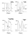
- Some examples of possible waveforms are shown in Figures 2 to 5. Some waveform types that can be used are square, triangular, and sinusoidal.
- the circuit includes positive (+) and negative (-) input terminals 8 and 12 and a metal oxide varistor (MOV) 10 connected across the input terminals 8 and 12 to suppress any transients of over 370 V that appear.
- a diode 14 allows positively biased signals to pass and cuts off negatively biased signals. In the reverse bias mode, hardly any current flows, which saves power and the rest of the components.
- a transistor Q turns on, which allows current to flow through a diode 16 of an opto-coupler.
- the transistor Q and a zener diode 18 connected as shown have bias currents supplied from the signal through a resistor R2 connected between the input terminal 8 and a base of the transistor Q.
- the zener voltage of the zener diode 18 controls a steady current to flow through the transistor Q. This is due to the nearly constant voltage appearing across an output resistor R3 connected between an emitter of the transistor Q and the diode 16. Therefore, after the signal reaches this point it will only draw 3 to 4 mA, regardless of how much higher the signal goes.
- This current through the opto-coupler diode 16 will cause a transistor 20 of the opto-coupler (which is optically coupled to the diode 16) to conduct, thereby pulling low the input to an inverter with Schmitt trigger circuit 22 (type 74HC14 circuit) connected to a collector of the transistor 20.
- the 74HC14 type circuit 22 has a Schmitt trigger input which provides the hysteresis necessary to keep noise from causing false pulses.
- the inverted output of the 74HC14 type circuit 22 is taken to an input pin of a microprocessor 24 which uses the signal for some industrial control function.
- the microprocessor 24 can sense these changes in level (edge-triggered interrupts). These interrupts can mark time be keeping track of the counts between them. Since there is a known internal clock frequency, the interrupt frequency can be determined. In a dc digital control input situation, one can determine if the level is high or low from reading the port or by keeping track of the transition state.
- ac line digital control input signals can be realised by using the frequency mode.
- An ac line signal can be recognized as a 45 to 65 Hz frequency for a high level signal and less than this for a low level signal.
- the frequency can be determined in half of a cycle. Another approach for determining the frequency is to count the transitions in a fixed period of time; however, this will not give quick results.
- a resistor R1 is connected between the positive input terminal 8 and a collector of the transistor Q for protecting the collector against surged current.
- a resistor R5 is connected between a base and an emitter of the opto-coupler transistor 20 for reducing noise, and for evening out opto-coupler on- off switching times.
- the opto-coupler 16, 20 can, for example, be a 4N36 type circuit, which is generally available in the industry.
- the microprocessor 24 requires a 0-5 V digital signal to sense the input control signal and provide adequate control to devices connected to the microprocessor.
- the MOV 10 prevents transients and noise spikes, while the zener diode 18 sets the voltage for the transistor Q, which requires a control voltage to operate and itself set up a constant current to the opto-coupler 16, 20.
- the digital/frequency input circuit described above has many advantages over prior arrangements.
- circuit doubles as a digital and/or frequency input circuit, additional circuitry such as frequency-to-voltage converters or ac coupled configurations are not required.
- the circuit limits the current input to 3 to 4 mA, which greatly reduces power consumption when high voltages are applied. For instance, if the voltage applied increased from 24 Vdc to 125 Vdc, the power in a standard resistive input circuit would go up by over 27 times for the value at which it started; whereas in the above-described circuit it would go up only by a factor of about 5.
- the above-described circuit typically pulls (draws) 3 to 4 mA. It requires a minimum current to activate the high level state; thus, this will provide some inherent noise immunity.
- the 74HC14 type circuit 22 with its Schmitt trigger input builds in hysteresis which helps prevent output oscillation during level transitions.
- the resistor R5 helps reduce noise from activating the opto-coupler.
- This circuit can be applied to a variety of input ranges and sensitivity levels by changing the values of the resistors R1, R2, R3 and the zener voltage of the zener diode 18. This would redefine the threshold voltages and input current limiting values.
Landscapes
- Engineering & Computer Science (AREA)
- Computer Networks & Wireless Communication (AREA)
- Signal Processing (AREA)
- Power Engineering (AREA)
- Physics & Mathematics (AREA)
- Electromagnetism (AREA)
- Manipulation Of Pulses (AREA)
- Electronic Switches (AREA)
- Measurement Of Current Or Voltage (AREA)
Abstract
Description
- This invention relates in general to signal conditioning or processing, for example for use in industrial control applications, and in particular to circuits for receiving and conditioning a variety of signals.
- Industrial digital and frequency input circuits normally are resistive circuits with opto-coupling for the required isolation. They are able to take a standard control signal such as 24 Vdc, 125 Vdc, 117 Vac, or 230 Vac.
- A drawback to these circuits is that they require jumper settings to select a desired signal range. Otherwise, the circuits are limited to only one signal type. A common problem is that customers end up with the jumpers in the wrong positions for their application, whereby failure occurs.
- Another problem with a resistive input circuit is that, as the applied voltage is increased, the power consumption increases at an accelerated rate. Also, there is a limit to signal knowledge depending on the method of monitoring. For example, if the level is checked ten times per second, it may be adequate for a digital input; however, a 5 Hz frequency is the highest it would be able to pick up according to Shannon's sampling theorem. On the other hand, if it is monitored at smaller increments like 20,000 times per second, then there probably would not be much time to do anything else. At this point a frequency-to-voltage converter may seem appealing; however, this requires an analogue signal measurement which is indirect and more difficult to implement.
- According to one aspect of the invention there is provided a circuit for conditioning a signal that may have a variety of waveforms and voltage levels, the circuit comprising:
a pair of input terminals for receiving the signal;
non-linear voltage limiting means connected across the input terminals for limiting any high transient voltage across the terminals;
a diode connected to one of the terminals for preventing a flow of reverse current to said one terminal;
a transistor having a base connected through a resistor to the other one of the terminals; and
opto-coupler means connected to an emitter of the transistor for receiving current therefrom, the opto-coupler means having an isolated output for outputting a conditioned signal. - The signal received by the circuit is preferably a control signal and the outputted conditioned signal is preferably for use in an industrial control application.
- According to another aspect of the invention there is provided an input circuit for industrial control applications, the circuit including a metal oxide varistor connected between input terminals of the circuit, a diode connected to one of the input terminals for preventing a negative current flow, and a zener diode connected across the input terminals for limiting voltage supplied to a transistor which has a base connected to one of the input terminals and which is connected to an opto-coupler. The opto-coupler preferably has an output connected to a Schmitt trigger input of an inverter, and an output of the inverter is preferably connected to a microprocessor or other apparatus for receiving an industrial control signal.
- A circuit according to a preferred embodiment of the invention, described in detail below, is capable of receiving a wide range of dc and ac voltages, thus eliminating the need for jumpers.
- The invention will not be further described, by way of illustrative and non-limiting example, with reference to the accompanying drawings, in which:
- Figure 1 is a schematic diagram of an input circuit according to a preferred embodiment of the invention;
- Figure 2 is a waveform diagram showing at the top the waveform of a possible input control signal and showing at the bottom the waveform of the signal after it has been conditioned by the input circuit for use by a microprocessor or other industrial control apparatus;
- Figure 3 is a view similar to Figure 2, showing another input control signal;
- Figure 4 is a view similar to Figure 2, showing a still further input control signal; and
- Figure 5 is a view similar to Figure 2, showing a possible non-standard input control signal.
- The drawings show an input circuit (control circuit) embodying the invention for receiving and conditioning input control signals having a wide variety of waveform and voltage, and for supplying the signals to a microprocessor or other industrial control apparatus. The input circuit is an improved digital/frequency input circuit which is designed for industrial control applications. A diagram of the circuit is shown in Figure 1.
- The circuit allows a wide range of standard and non-standard control signals to be applied. When tested, it had a minimum high level threshold voltage of 11 V and a low level maximum of 8 V for a 0 to 10 kHz signal. The circuit is capable of withstanding an input voltage of 130 Vdc and 250 Vac. Therefore, it can handle any dc control signals from about 15 V to 250 V. Some of the standard control input signals this will accommodate are 15 Vdc, 24 Vdc, 28 Vdc, 125 Vdc, 24 Vac, 117 Vac, and 230 Vac. All of these signals can be applied without the need to use jumpers to select the range. The only criteria for the input signal are that it is above 15 V for high level and below 2 V for low level while at the same time not exceeding +130 Vdc, 250 Vac or going negative by more than -350 Vdc. The signal frequency limit was tested up to about 45 kHz; however, 10 kHz is good enough for most control signal applications. Therefore, practically any waveform shape that holds to these criteria may be used successfully.
- Some examples of possible waveforms are shown in Figures 2 to 5. Some waveform types that can be used are square, triangular, and sinusoidal.
- Looking in more detail at Figure 1, the circuit includes positive (+) and negative (-)
input terminals input terminals diode 16 of an opto-coupler. The transistor Q and azener diode 18 connected as shown have bias currents supplied from the signal through a resistor R2 connected between theinput terminal 8 and a base of the transistor Q. Once the zener voltage of thezener diode 18 is reached, it controls a steady current to flow through the transistor Q. This is due to the nearly constant voltage appearing across an output resistor R3 connected between an emitter of the transistor Q and thediode 16. Therefore, after the signal reaches this point it will only draw 3 to 4 mA, regardless of how much higher the signal goes. - This current through the opto-
coupler diode 16 will cause a transistor 20 of the opto-coupler (which is optically coupled to the diode 16) to conduct, thereby pulling low the input to an inverter with Schmitt trigger circuit 22 (type 74HC14 circuit) connected to a collector of the transistor 20. The74HC14 type circuit 22 has a Schmitt trigger input which provides the hysteresis necessary to keep noise from causing false pulses. The inverted output of the74HC14 type circuit 22 is taken to an input pin of amicroprocessor 24 which uses the signal for some industrial control function. - As the applied control signal drops, it will reach a point where the current through the resistor R3 and the opto-
coupler 16, 20 is such that it allows a pull-up resistor R4 (connected as shown between a +5 Vdc supply and the circuit 22) to raise the input voltage to thecircuit 22, which causes the inverted output thereof to go low. Themicroprocessor 24 can sense these changes in level (edge-triggered interrupts). These interrupts can mark time be keeping track of the counts between them. Since there is a known internal clock frequency, the interrupt frequency can be determined. In a dc digital control input situation, one can determine if the level is high or low from reading the port or by keeping track of the transition state. - ac line digital control input signals can be realised by using the frequency mode. An ac line signal can be recognized as a 45 to 65 Hz frequency for a high level signal and less than this for a low level signal. For 50/50 duty cycle waveforms, the frequency can be determined in half of a cycle. Another approach for determining the frequency is to count the transitions in a fixed period of time; however, this will not give quick results.
- As shown in Figure 1, a resistor R1 is connected between the
positive input terminal 8 and a collector of the transistor Q for protecting the collector against surged current. A resistor R5 is connected between a base and an emitter of the opto-coupler transistor 20 for reducing noise, and for evening out opto-coupler on- off switching times. - The opto-
coupler 16, 20 can, for example, be a 4N36 type circuit, which is generally available in the industry. - The
microprocessor 24 requires a 0-5 V digital signal to sense the input control signal and provide adequate control to devices connected to the microprocessor. - The
MOV 10 prevents transients and noise spikes, while thezener diode 18 sets the voltage for the transistor Q, which requires a control voltage to operate and itself set up a constant current to the opto-coupler 16, 20. - The digital/frequency input circuit described above has many advantages over prior arrangements.
- The elimination of physical jumpers in the circuit eliminates the need for a customer to set the jumpers. Not only does this free the customer from the need to consult documentation on jumper positions, but it helps prevent failure due to incorrect jumper settings.
- Since the above-described circuit is practically waveform independent, this gives the customer the flexibility of running sinusoidal signals, square wave (on-off dc signals), or non-standard signals such as a triangular signal, if so desired.
- Since the circuit doubles as a digital and/or frequency input circuit, additional circuitry such as frequency-to-voltage converters or ac coupled configurations are not required.
- The circuit limits the current input to 3 to 4 mA, which greatly reduces power consumption when high voltages are applied. For instance, if the voltage applied increased from 24 Vdc to 125 Vdc, the power in a standard resistive input circuit would go up by over 27 times for the value at which it started; whereas in the above-described circuit it would go up only by a factor of about 5.
- The above-described circuit typically pulls (draws) 3 to 4 mA. It requires a minimum current to activate the high level state; thus, this will provide some inherent noise immunity. The
74HC14 type circuit 22 with its Schmitt trigger input builds in hysteresis which helps prevent output oscillation during level transitions. The resistor R5 helps reduce noise from activating the opto-coupler. - This circuit can be applied to a variety of input ranges and sensitivity levels by changing the values of the resistors R1, R2, R3 and the zener voltage of the
zener diode 18. This would redefine the threshold voltages and input current limiting values.
Claims (11)
a pair of input terminals (8, 12) for receiving the signal;
non-linear voltage limiting means (10) connected across the input terminals (8, 12) for limiting any high transient voltage across the terminals;
a diode (14) connected to one (12) of the terminals (8,12) for preventing a flow of reverse current to said one terminal (12);
a transistor (Q) having a base connected through a resistor (R2) to the other one (8) of the terminals (8,12); and
opto-coupler means (16, 20) connected to an emitter of the transistor (Q) for receiving current therefrom, the opto-coupler means having an isolated output for outputting a conditioned signal.
Applications Claiming Priority (2)
| Application Number | Priority Date | Filing Date | Title |
|---|---|---|---|
| US07/340,984 US5068545A (en) | 1989-04-20 | 1989-04-20 | Digital/frequency input for industrial control applications |
| US340984 | 1994-11-17 |
Publications (3)
| Publication Number | Publication Date |
|---|---|
| EP0393282A2 true EP0393282A2 (en) | 1990-10-24 |
| EP0393282A3 EP0393282A3 (en) | 1991-08-21 |
| EP0393282B1 EP0393282B1 (en) | 1995-04-12 |
Family
ID=23335769
Family Applications (1)
| Application Number | Title | Priority Date | Filing Date |
|---|---|---|---|
| EP89312673A Expired - Lifetime EP0393282B1 (en) | 1989-04-20 | 1989-12-05 | Signal conditioning circuits |
Country Status (7)
| Country | Link |
|---|---|
| US (1) | US5068545A (en) |
| EP (1) | EP0393282B1 (en) |
| JP (1) | JPH02295312A (en) |
| AU (1) | AU626038B2 (en) |
| CA (1) | CA2002791C (en) |
| DE (1) | DE68922210T2 (en) |
| NO (1) | NO894448L (en) |
Cited By (5)
| Publication number | Priority date | Publication date | Assignee | Title |
|---|---|---|---|---|
| EP0949759A1 (en) * | 1998-04-09 | 1999-10-13 | Electrowatt Technology Innovation AG | Apparatus for generating an output voltage from an input voltage in an electricity meter, a remote control receiver, a combination of both and/or an additional device for use therewith, the output signal having a defined level which is independent from the level of the input signal |
| EP1873915A3 (en) * | 2006-06-28 | 2008-05-28 | Phoenix Contact GmbH & Co. KG | Secure input circuit with single channel peripheral connection for the input of a bus participant |
| DE102011015498A1 (en) * | 2011-03-29 | 2012-10-04 | Phoenix Contact Gmbh & Co. Kg | Input circuit for an input module and method for operating an input circuit |
| EP3079259A1 (en) * | 2015-04-06 | 2016-10-12 | Rockwell Automation Technologies, Inc. | Low-power dissipation input circuit |
| CN109831204A (en) * | 2018-12-13 | 2019-05-31 | 深圳市崧盛电子股份有限公司 | A kind of signal isolation conversion circuit and control device |
Families Citing this family (13)
| Publication number | Priority date | Publication date | Assignee | Title |
|---|---|---|---|---|
| US5239209A (en) * | 1991-06-17 | 1993-08-24 | Minnesota Mining And Manufacturing Company | Zero crossing detection circuit |
| JPH0537322A (en) * | 1991-07-30 | 1993-02-12 | Nippondenso Co Ltd | Output circuit for control signal |
| JPH0582876A (en) * | 1991-09-18 | 1993-04-02 | Minolta Camera Co Ltd | Laser diode unit driving method |
| JPH06195476A (en) * | 1992-07-21 | 1994-07-15 | Advanced Micro Devicds Inc | Integrated circuit for incorporation of microcontroller and method for reduction of power consumption by it |
| US5570263A (en) * | 1994-12-27 | 1996-10-29 | Dataserv Computer Maintenance, Inc. | Communications bus surge protector |
| US5539352A (en) * | 1994-12-28 | 1996-07-23 | General Electric Company | Low power voltage input circuit with high noise immunity and fast operating time |
| KR0143434B1 (en) * | 1995-01-09 | 1998-08-17 | 신재인 | High peak power pulse generation in lamp pumped continuous wave lasers by current mixing |
| US5789960A (en) * | 1996-09-04 | 1998-08-04 | Control Gaging, Inc. | Universal input circuit including opto-isolator and retriggerable monostable multivibrator |
| US5805062A (en) * | 1996-10-21 | 1998-09-08 | Mini-Systems, Inc. | 2-wire optovoltaic loop-powered isolation amplifier with current bootstrapping |
| EP1078304B1 (en) | 1998-05-20 | 2003-07-16 | The Foxboro Company | Self-validating output module |
| CN102073108B (en) * | 2010-11-29 | 2013-11-06 | 华为终端有限公司 | Optical coupler isolating circuit |
| CN102497197A (en) * | 2011-12-28 | 2012-06-13 | 中冶南方(武汉)自动化有限公司 | Isolated bidirectional digital input output circuit |
| JP2019087938A (en) * | 2017-11-09 | 2019-06-06 | ルネサスエレクトロニクス株式会社 | Semiconductor device, semiconductor system, and control method of semiconductor device |
Family Cites Families (10)
| Publication number | Priority date | Publication date | Assignee | Title |
|---|---|---|---|---|
| JPS5242010B1 (en) * | 1971-06-14 | 1977-10-21 | ||
| US4063045A (en) * | 1976-07-27 | 1977-12-13 | Extel Corporation | Telecommunication line switching circuit |
| JPS5464452A (en) * | 1977-11-01 | 1979-05-24 | Fuji Electric Co Ltd | Signal selection unit using photo coupling circuit |
| US4321487A (en) * | 1980-04-07 | 1982-03-23 | Reliance Electric Company | Common mode rejection coupler |
| US4484331A (en) * | 1981-07-20 | 1984-11-20 | Rca Corporation | Regulator for bias current of semiconductor laser diode |
| DE3322896A1 (en) * | 1983-06-23 | 1985-01-03 | Siemens AG, 1000 Berlin und 8000 München | CIRCUIT ARRANGEMENT FOR POTENTIAL-FREE DETECTION OF BINARY ELECTRICAL SIGNALS |
| JPS6074807A (en) * | 1983-09-30 | 1985-04-27 | Toshiba Corp | Converting circuit |
| US4645948A (en) * | 1984-10-01 | 1987-02-24 | At&T Bell Laboratories | Field effect transistor current source |
| JPS62110317A (en) * | 1985-11-08 | 1987-05-21 | Toshiba Corp | Solid-state relay |
| JPS62188525A (en) * | 1986-02-14 | 1987-08-18 | Mitsubishi Electric Corp | signal transmission equipment |
-
1989
- 1989-04-20 US US07/340,984 patent/US5068545A/en not_active Expired - Fee Related
- 1989-11-08 NO NO89894448A patent/NO894448L/en unknown
- 1989-11-10 CA CA002002791A patent/CA2002791C/en not_active Expired - Fee Related
- 1989-12-05 DE DE68922210T patent/DE68922210T2/en not_active Expired - Fee Related
- 1989-12-05 EP EP89312673A patent/EP0393282B1/en not_active Expired - Lifetime
-
1990
- 1990-04-19 AU AU53735/90A patent/AU626038B2/en not_active Ceased
- 1990-04-20 JP JP2103303A patent/JPH02295312A/en active Pending
Cited By (10)
| Publication number | Priority date | Publication date | Assignee | Title |
|---|---|---|---|---|
| EP0949759A1 (en) * | 1998-04-09 | 1999-10-13 | Electrowatt Technology Innovation AG | Apparatus for generating an output voltage from an input voltage in an electricity meter, a remote control receiver, a combination of both and/or an additional device for use therewith, the output signal having a defined level which is independent from the level of the input signal |
| EP1873915A3 (en) * | 2006-06-28 | 2008-05-28 | Phoenix Contact GmbH & Co. KG | Secure input circuit with single channel peripheral connection for the input of a bus participant |
| US7719255B2 (en) | 2006-06-28 | 2010-05-18 | Phoenix Contact Gmbh & Co. Kg | Safe input circuit with one-channel peripheral connection for the input of a bus participant |
| EP2378663A3 (en) * | 2006-06-28 | 2012-01-04 | PHOENIX CONTACT GmbH & Co. KG | Secure input circuit with single channel peripheral connection for the input of a bus participant |
| DE102011015498A1 (en) * | 2011-03-29 | 2012-10-04 | Phoenix Contact Gmbh & Co. Kg | Input circuit for an input module and method for operating an input circuit |
| DE102011015498B4 (en) * | 2011-03-29 | 2012-10-25 | Phoenix Contact Gmbh & Co. Kg | Input circuit for an input module and method for operating an input circuit |
| EP2506436A3 (en) * | 2011-03-29 | 2013-05-22 | Phoenix Contact GmbH & Co. KG | Input circuit for an input component and method for operating same |
| EP3079259A1 (en) * | 2015-04-06 | 2016-10-12 | Rockwell Automation Technologies, Inc. | Low-power dissipation input circuit |
| US10158358B2 (en) | 2015-04-06 | 2018-12-18 | Rockwell Automation Technologies, Inc. | Low-power dissipation input circuit |
| CN109831204A (en) * | 2018-12-13 | 2019-05-31 | 深圳市崧盛电子股份有限公司 | A kind of signal isolation conversion circuit and control device |
Also Published As
| Publication number | Publication date |
|---|---|
| JPH02295312A (en) | 1990-12-06 |
| CA2002791C (en) | 1996-06-18 |
| EP0393282A3 (en) | 1991-08-21 |
| EP0393282B1 (en) | 1995-04-12 |
| NO894448D0 (en) | 1989-11-08 |
| US5068545A (en) | 1991-11-26 |
| DE68922210D1 (en) | 1995-05-18 |
| CA2002791A1 (en) | 1990-10-20 |
| AU5373590A (en) | 1990-10-25 |
| AU626038B2 (en) | 1992-07-23 |
| DE68922210T2 (en) | 1995-08-17 |
| NO894448L (en) | 1990-10-22 |
Similar Documents
| Publication | Publication Date | Title |
|---|---|---|
| EP0393282B1 (en) | Signal conditioning circuits | |
| JPH087241B2 (en) | Signal processing circuit and converter circuit | |
| EP0097559B1 (en) | Autofunction voltmeter | |
| EP1180840A2 (en) | Power supply negative phase detecting circuit | |
| EP0298737A1 (en) | Solenoid drive circuit | |
| US4356442A (en) | Electronic voltage and continuity testing unit | |
| EP0247654A2 (en) | Noise immune circuit for use with frequency sensor | |
| EP0092807B1 (en) | A digital supervisory circuit for a telephone system | |
| US4031417A (en) | Apparatus for coupling a digital data generator to a digital data readout device with electrical isolation therebetween | |
| EP0283030A2 (en) | Device for measuring amount of engine suction air | |
| JPH06113553A (en) | Ac adapter | |
| CN109839547B (en) | Three-phase power phase sequence detection circuit | |
| GB2249840A (en) | Universal digital input channel | |
| KR100352598B1 (en) | Apparatus for automatical controlling input of digital mult imeter | |
| EP0268378A2 (en) | A phonic meter for measuring current/force/resistance | |
| JPS59152028A (en) | Resistivity control device for electrical discharge machining | |
| KR950002410Y1 (en) | Overcurrent Protection Circuit of Sensor for Detection | |
| JPH04276226A (en) | Dust detection device for vacuum cleaner | |
| SU1104429A1 (en) | Ac-to-dc voltage measuring converter | |
| JPS59100882A (en) | Device for detecting number of poles and rotating direction of motor | |
| KR100242780B1 (en) | Digital timing relay | |
| SU1550610A1 (en) | Threshold device | |
| JPH01140848A (en) | Alternating current signal receiver | |
| KR920000253Y1 (en) | Open state sensing device for motor flywheel diode | |
| JPH09103088A (en) | Motor drive circuit |
Legal Events
| Date | Code | Title | Description |
|---|---|---|---|
| PUAI | Public reference made under article 153(3) epc to a published international application that has entered the european phase |
Free format text: ORIGINAL CODE: 0009012 |
|
| AK | Designated contracting states |
Kind code of ref document: A2 Designated state(s): DE FR GB IT |
|
| RAP1 | Party data changed (applicant data changed or rights of an application transferred) |
Owner name: INTERNATIONAL CONTROL AUTOMATION FINANCE S.A. |
|
| PUAL | Search report despatched |
Free format text: ORIGINAL CODE: 0009013 |
|
| AK | Designated contracting states |
Kind code of ref document: A3 Designated state(s): DE FR GB IT |
|
| 17P | Request for examination filed |
Effective date: 19920120 |
|
| 17Q | First examination report despatched |
Effective date: 19940304 |
|
| GRAA | (expected) grant |
Free format text: ORIGINAL CODE: 0009210 |
|
| AK | Designated contracting states |
Kind code of ref document: B1 Designated state(s): DE FR GB IT |
|
| REF | Corresponds to: |
Ref document number: 68922210 Country of ref document: DE Date of ref document: 19950518 |
|
| ET | Fr: translation filed | ||
| ITF | It: translation for a ep patent filed | ||
| PLBE | No opposition filed within time limit |
Free format text: ORIGINAL CODE: 0009261 |
|
| STAA | Information on the status of an ep patent application or granted ep patent |
Free format text: STATUS: NO OPPOSITION FILED WITHIN TIME LIMIT |
|
| 26N | No opposition filed | ||
| PGFP | Annual fee paid to national office [announced via postgrant information from national office to epo] |
Ref country code: FR Payment date: 19961115 Year of fee payment: 8 |
|
| PGFP | Annual fee paid to national office [announced via postgrant information from national office to epo] |
Ref country code: DE Payment date: 19961122 Year of fee payment: 8 |
|
| PGFP | Annual fee paid to national office [announced via postgrant information from national office to epo] |
Ref country code: GB Payment date: 19961128 Year of fee payment: 8 |
|
| PG25 | Lapsed in a contracting state [announced via postgrant information from national office to epo] |
Ref country code: GB Free format text: LAPSE BECAUSE OF NON-PAYMENT OF DUE FEES Effective date: 19971205 |
|
| PG25 | Lapsed in a contracting state [announced via postgrant information from national office to epo] |
Ref country code: FR Free format text: THE PATENT HAS BEEN ANNULLED BY A DECISION OF A NATIONAL AUTHORITY Effective date: 19971231 |
|
| GBPC | Gb: european patent ceased through non-payment of renewal fee |
Effective date: 19971205 |
|
| PG25 | Lapsed in a contracting state [announced via postgrant information from national office to epo] |
Ref country code: DE Free format text: LAPSE BECAUSE OF NON-PAYMENT OF DUE FEES Effective date: 19980901 |
|
| REG | Reference to a national code |
Ref country code: FR Ref legal event code: ST |
|
| PG25 | Lapsed in a contracting state [announced via postgrant information from national office to epo] |
Ref country code: IT Free format text: LAPSE BECAUSE OF NON-PAYMENT OF DUE FEES Effective date: 20051205 |