EP0393080B1 - Hypersystolic reed-solomon encoder - Google Patents
Hypersystolic reed-solomon encoder Download PDFInfo
- Publication number
- EP0393080B1 EP0393080B1 EP88909680A EP88909680A EP0393080B1 EP 0393080 B1 EP0393080 B1 EP 0393080B1 EP 88909680 A EP88909680 A EP 88909680A EP 88909680 A EP88909680 A EP 88909680A EP 0393080 B1 EP0393080 B1 EP 0393080B1
- Authority
- EP
- European Patent Office
- Prior art keywords
- message
- symbols
- stream
- cell
- cells
- Prior art date
- Legal status (The legal status is an assumption and is not a legal conclusion. Google has not performed a legal analysis and makes no representation as to the accuracy of the status listed.)
- Expired - Lifetime
Links
Images


Classifications
-
- H—ELECTRICITY
- H03—ELECTRONIC CIRCUITRY
- H03M—CODING; DECODING; CODE CONVERSION IN GENERAL
- H03M13/00—Coding, decoding or code conversion, for error detection or error correction; Coding theory basic assumptions; Coding bounds; Error probability evaluation methods; Channel models; Simulation or testing of codes
- H03M13/03—Error detection or forward error correction by redundancy in data representation, i.e. code words containing more digits than the source words
- H03M13/05—Error detection or forward error correction by redundancy in data representation, i.e. code words containing more digits than the source words using block codes, i.e. a predetermined number of check bits joined to a predetermined number of information bits
- H03M13/13—Linear codes
- H03M13/15—Cyclic codes, i.e. cyclic shifts of codewords produce other codewords, e.g. codes defined by a generator polynomial, Bose-Chaudhuri-Hocquenghem [BCH] codes
-
- H—ELECTRICITY
- H03—ELECTRONIC CIRCUITRY
- H03M—CODING; DECODING; CODE CONVERSION IN GENERAL
- H03M13/00—Coding, decoding or code conversion, for error detection or error correction; Coding theory basic assumptions; Coding bounds; Error probability evaluation methods; Channel models; Simulation or testing of codes
- H03M13/03—Error detection or forward error correction by redundancy in data representation, i.e. code words containing more digits than the source words
- H03M13/033—Theoretical methods to calculate these checking codes
Abstract
Description
- Error detection and correction systems remove errors introduced into data traveling through a channel from a transmitter to a receiver.
- In such a system, the transmitter appends to each set of message symbols a set of redundant check symbols in accordance with a code generator polynomial G(Z) known to both the transmitter and the receiver. The codeword thus generated contains sufficient information for the receiver to correct errors introduced during transit through the channel, as long as the number of erroneous symbols does not exceed half the number of check characters, using Reed-Solomon codes, for example. Such error detection and correction systems are useful over a wide variety of digital systems including digital recording systems, digital memory systems and digital communications systems.
- One type of error detection and correction system uses Reed-Solomon codes to construct the redundant check characters (encode) at the transmitter and to correct errors (decode) at the receiver. The transmitter computes the redundant check symbols from the set of message characters using a standard Reed-Solomon encoder.
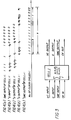
- Referring to Fig. 1, a standard Reed-Solomon encoder includes an
input node 10 which receives the stream of message symbols in serial succession, and anoutput node 12 from which the redundant check characters are transmitted following the end of the stream of message symbols. Between the input andoutput nodes stages 14, Galoisfield adders 16 and Galoisfield multipliers 18. Each of the Galoisfield multipliers 18 multiplies the feedback signal by a particular one of the coefficients gi of the code generator polynomial G(Z), as illustrated in Fig. 1. In the Reed-Solomon encoder of Fig. 1, the number of stages in the shift register is precisely equal to R, the number of redundant check characters. - The problem with the standard Reed-Solomon encoder of Fig. 1 is twofold, namely: (a) Timing constraints: The feedback network requires all of the
stages 14 to operate synchronously. This in turn requires a central (global) clock, which must be distributed to all of the stages. Such distribution entails long connections or a complex distribution scheme, either of which slows down the system, due to inevitable clock skews created by the distribution network. And (b) Inflexibility: a significant hardware change is required whenever it is desired to change the number R of redundant check characters to be appended to the block of K message symbols. - The problem is how to implement a more flexible Reed-Solomon encoder which is systematic (i.e., it reproduces the stream of message symbols immediately followed by a stream of redundant check symbols), which does not have global signals, and which is faster than currently available encoders.
- One known way of attacking the problem is so-called "transform" encoding and decoding which has the advantage of not requiring any feedback among each of the cells of the shift register. The transform encoder lends itself to a systolic implementation, i.e., an implementation without feedback or global signals in which each cell is connected only to its immediate neighbors. Each symbol in a codeword generated by such a transform encoder is a linear combination of all symbols in the original message. The disadvantages of such transform encoding are: (a) the number of encoder cells (shift register stages) is equal to K, the number of message symbols in each block (which usually is far greater than the number R of cells required in Fig. 1) and (b) the encoding is non-systematic, in that the message and redundancy information is distributed among the K + R codeword symbols generated by the transform encoder, so that the encoder does not output an exact copy of the original message (which complicates the decoding process). Thus, because the transform encoder requires K-R more cells than the standard Reed-Solomon encoder and because it is non-systematic, it is not really a solution to the problem.
- In IEEE Transactions on Computers, Vol. C-34, No. 5, May 1985, pages 393 - 403, a Pipeline Reed-Solomon Decoder is disclosed showing a systolic systematic circuit (Fig. 2) used for syndrome calculation for a Reed-Solomon code. This circuit comprises R substantially identical successive cells for Galois Field Arithmetic calculation for calculating syndromes of an RS-code for error correction.
- Although such a circuit may also be useable for encoding of a stream of message symbols, in this circuit all the Galois Field Arithmetic has to be performed within the successive cells, which results in downslowing of the encoding procedure.
- The present invention is a highly flexible systolic systematic Reed-Solomon encoder having R stages which operate independently of each other (so that the encoder is systolic) and receive and pass on (without alteration) each of the message symbols before appending a redundant check symbol at the end of the message stream (so that the encoder is systematic). The encoder comprises a set of identical modular cells quickly reconfigurable to adjust for changes in the number R of check symbols to be appended to a given block of message symbols (so that the encoder is flexible).
- It is a discovery of the invention that there is an algorithm which can be performed at each stage of an R-stage encoder without reference to any of the computations performed in the other stages, to generate an individual one of the R redundant check symbols. There is no feedback between any of the individual cells using such an algorithm, and the operation is systolic and systematic. The algorithm is adapted in each individual one of the R stages by selecting the values of two constants in the algorithm, as will be described. Otherwise, each of the cells defining the stages in the encoder shift register are identical in their hardware configuration and operation, facilitating a significant cost savings. Because each cell is independent from each of the other cells, the systolic array of cells is readily adaptable to changes in the number R of check symbols to be appended to the block of message characters.
- The jth cell of the R systolic encoder cells performs the following operation on each of the K message symbols ui to compute the jth redundant check symbol wj:

where j obeys the following: 1≦j≦R.
Each of the quantities ci and xi are defined below in this specification; they change each time a different message symbol ui is received in the cell. The quantities dj and yj are quantities which are constant within the jth cell and are also defined below in the specification. Such a cell is called a Cauchy cell, in accordance with the class of mathematical operations it performs which are described in Seroussi and Roth, "On Generator Matrices of MDS Codes," IEEE Transactions on Information Theory, November 1985, pp. 826-830. - In operation, the cells are arranged in serial order and process each succeeding message symbol ui in order of receipt, passing the current message symbol to its neighboring downstream cell while receiving the next message symbol from its neighboring upstream cell. As the last message symbol uk leaves the jth cell and enters the j+1st cell, the jth cell completes its computation of the redundant message symbol wj and appends wj to the end of the message stream. In this manner, a complete set of R redundant check symbols (w₁ through wR) are appended at the end of the message stream of K message symbols as the array of R cells systolically processes the message symbol block.
- Each cell may be enabled or disabled in real time so that it either appends or does not append its computed redundant check symbol to the message stream. In this manner, the number R of active cells (which determines the number R of appended redundant check symbols) may be increased or decreased in real time in accordance with any desired change in R. Furthermore, the operation of the systolic array of Cauchy cells of the invention is independent of the number K of message symbols, so that the systolic array of Cauchy cells of this invention can accommodate in real time changes in K, the number of message symbols and/or R, the number of redundant check symbols in each code word.
- When the encoder has a global signal (e.g. the feedback path), that signal needs to be generated at one cell and synchronously clocked to a plurality of other cells. This forces a synchronous design with a global clock.
- Elimination of the feedback path (and any other global signals) permits a systolic clock distribution method, by which each cell receives an input clock signal (say CK_IN) from its predecessor cell, electrically buffers it, and propogates it through an output clock signal (say CK_OUT) to its successor cell. The fact that the clock is also systolic is denoted by the "hyper" prefix (hence, the term "hypersystolic encoder"). Systolic arrays found in the literature have a central (global) clock, which needs to be distributed to all the cells through some kind of distribution net. As mentioned above, this implies the need for either long connections or a complex distribution scheme, which in any case slow down the system, due to the inevitable clock skews created by the distribution net. In a hypersystolic system, clock distribution is ideal: a very short clock line from one cell to the next.
- Also, in the hypersystolic system of the invention, while neighboring cells may be regarded as synchronous (they exchange data through a common clock that is transmitted from one to the next), the system as a whole is asynchronous, due to the clock skew caused by the passage of the clock signal through each cell. When one looks at two cells that are not immediate neighbors (say, three or four cells apart), the accumulated clock skew is large enough so that they may be considered asynchronous (i.e. the clock signals are in random phase with respect to each other).
- The hypersystolic encoder may therefore operate at extremely high data rates, on the order of several gigabits/second, which are extremely difficult if not impossible to attain with standard designs.
- The invention may be understood by reference to the accompanying drawings, of which:
- Fig. 1 is a simplified block diagram of a prior art Reed-Solomon encoder;
- Fig. 2 is a simplified block diagram of the hypersystolic Reed-Solomon encoder of the invention;
- Fig. 3 is a simplified block diagram of an individual cell in the encoder of Fig. 2;
- Fig. 4a-4e include contemporaneous timing diagrams illustrating operation of the hypersystolic Reed-Solomon encoder of Fig. 2;
- Figs. 5a and 5b illustrate the uici processor used in the hypersystolic encoder of Fig. 2;
- Figs. 6a, 6b and 6c are detailed block diagrams of the cell of Fig. 3; and
- Figs. 7a-7h include contemporaneous timing diagrams of signals controlling operation of the cell of Fig. 3.
- Referring to Fig. 2, a uici processor 20 receives at its input a stream of message symbols ui in synchronism with a clock signal CK. The
processor 20 transmits at its output a delayed version of the stream of message symbols ui and a buffered version of the clock signal CK. In addition, theprocessor 20 outputs the product uici to be defined below. These three results are passed to a systolic array of identicalCauchy cells 22. This array processes the stream of message symbols ui and products uici systolically in synchronism with the hypersystolic clock signal CK and adds a stream of check characters at the end of the message stream. Each of the cells has the form illustrated in Fig. 3, including a UC input, a U input, an SMC input, a CK_IN input, a UC output, a U output, an SMC output and a CK_OUT output. The jth one of the R cells, for example, performs the algorithm indicated in Fig. 3 using all of the message symbols ui through uK and constants dj and yj to be defined below. - As soon as the last (Kth) message symbol uK has been received and processed in the jth cell, the computation performed by that cell of the jth redundant check symbol wj is complete, so that the jth cell outputs wj on its U output immediately following the last symbol in the message stream. The next symbol, of course, will be the check symbol wj-1 appended by the adjacent upstream neighbor cell (the j-1st cell).
- This is best illustrated in Fig. 4. In Fig. 4a, the SMC input of
cell number 1 constitutes a string of K logic "ones" (during the first K cycles of the clock signal CK) followed by a string of R logic "zeroes" (during the last R cycles of the clock signal CK). Thus, SMCi = 1 for i = 1 through K, and SMCi = 0 for i = K + 1 through K + R. The SMC signal serves to inform the cell when the transition from message to check symbols occurs. - Simultaneously, the U input of cell 1 (Fig. 4b) constitutes the K message symbols u₁ through UK for the first K cycles of the clock signal CK followed by R zeroes for the last R cycles of the clock signal CK. The U output of cell number 1 (Fig. 4c) is delayed with respect to the U input by one CK clock cycle and comprises the K message symbols u₁ through uK in order followed by the results of the computation performed in
cell number 1, namely the redundant check character w₁. This is followed in turn by R-1 zeroes. - The next cell, cell number 2 (whose output is not illustrated in Fig. 4) has an identical output, delayed with respect to the output of
cell 1 by one CK clock cycle, except that w₂ (computed in cell number 2) is inserted immediately before w₁. - Finally, as illustrated in Fig. 4d, the U output of cell R, the last cell in the systolic array of
cells 22, is delayed with respect to the output ofcell 1 by R clock cycles, and is in fact identical therewith for the first K clock cycles, but thereafter transmits all of the check characters w₁ through wR at the end of the message stream (wR being computed in cell R). The SMC output of cell R is identical with the SMC input ofcell 1 except that it is delayed by R clock cycles. - Each of the
Cauchy cells 22 must process all of the message symbols in the stream before it can generate a corresponding redundant check symbol to be added to the end of the stream. - In principle, Fig. 4 may be thought of as illustrating a process in which a long train (stream) of railroad cars (message symbols) is constantly supplemented "on the fly" with an additional railroad car (check symbol) as it passes through periodic stations (cells) along the railroad track, each station being responsible for inserting its own particular railroad car, until the last station adds the last additional railroad car to the train, and the process is complete.
- Referring to the algorithm of equation (1) on
page 4, ui is the ith message symbol in the stream of K message symbols. ui is an m-bit binary byte and the encoder of Fig. 2 uses a Reed-Solomon code of maximum length N = 2m-1 in a Galois field GF(2m) to compute the R redundant check symbols in accordance with a code generator polynomial G(Z). In the following definitions, a is a primitive element of the Galois field GF(2m). (See Elwyn R. Berlekamp, Algebraic Coding Theory, Academic Press, 1968.) The remaining symbols in the algorithm of equation (1) are defined as follows:
where 1≦i≦K,
where 1≦j≦R,
where 1≦i≦K,
where 1≦j≦R - In equations (1)-(5), K is the number of message bytes and the parameter a is defined as follows:

(i.e., a is the positive remainder from (1-L) ÷ N) where αL is the lowest order root of the code generator polynomial G(Z). (The quantity L is discussed in somewhat greater detail in U.S. Patent Application Serial No. 076,579 entitled "Hard-Wired Serial Galois Field Decoder" filed July 22, 1987 by Earl T. Cohen). - Referring to Fig. 2, each cell receives the product uici generated at the
processor 20, so that the cell is responsible for performing only a part of the computation of equation (1). There are R Cauchy cells which process the stream of products uici and there is an additional cell of different design used to implement the uici processor 20, for a total of R+1 cells. - An implementation of the uici processor 20 is illustrated in Fig. 5a. The
processor 20 includes a register 30 containing an m-bit byte equal to the first of the ci′s, namely c₁ (a constant). The definition of c₁ is denoted in Fig. 5a inside the register 30. This byte (c₁) is furnished to the "0" input of amultiplexer 32. The value of c₁ is loaded into the register 30 during system initialization and remains constant during operation. - The output of the
multiplexer 32 is applied to one input of aGalois field multiplier 34. The other input of theGalois field multiplier 34 receives an m-bit byte equal to the ratio ci+1/ci, by which each ci+1 may be computed from its predecessor, ci. This ratio is stored inregister 36 and is defined (as denoted in Fig. 5a inside the box 37) for each value of i in accordance with the following equation:
where the range of i is: 1≦i≦K-1 and the quantity "a" is as defined previously. The output of themultiplier 34 is applied to the input of aregister 38 whose output is applied to the "1" input of themultiplexer 32. - The
register 38 stores the output, ci+1, of themultiplier 34. ci₊₁ is present at the input of theregister 38 while, simultaneously, its predecessor ci is present at the output of theregister 38. Theregister 36 furnishes to themultiplier 34 the appropriate ratio ci+1/ci for each value of i. A logic circuit 37 (Fig. 5b) loads a new value of ci+1/ci into theregister 36 each time the index i is incremented. - The
logic circuit 37 computes the ratio ci+1/ci in accordance with equation (7) for each successive value of i. Fig. 5b illustrates one way the logic circuit may be implemented. A CSEL logic signal (Fig. 7g) causes amultiplexer 100 to select a constant αa+1 furnished to its 0 input from aregister 102 just before the receipt of the message stream. (Theregister 102 is programmed with the value of αa+1 during system initialization and remains constant during system operation.) Then, during receipt of the message stream, the CSEL logic signal causes the multiplexer to select at its 1 input the product furnished by aconstant multiplier 104. Theconstant multiplier 104 multiplies whatever value is present at its input by α⁻¹ in accordance with Galois field multiplication rules. This type of multiplier is described below in greater detail in connection with Fig. 6b. - The current output of the
multiplexer 100 is stored in aregister 106, whose contents is recirculated through the input of theconstant multiplier 104. The content of theregister 106 is the value of αa+1-i. AGalois field adder 108 combines this latter quantity with the value of a constant αa+1-K furnished from aregister 110. Theregister 110 is programmed with the value of αa+1-K during system initialization and remains constant during system operation. The output of theadder 108 is the numerator of the expression at the right hand side of equation (7). The denominator of this ratio is computed in a sub-circuit 102′, 104′, 106′, 108′, 110′ identical to the foregoingsub-circuit register 102′ is initialized with the value of α⁻¹ and theregister 110′ is initialized with the value of 1. TheGalois field divider 112 divides the numerator from theregister 108 by the denominator from theregister 108′ to generate the ratio ci+1/ci. - Operation is controlled by a
control logic circuit 40 in synchronism with the SMC signal and the clock signal CK received at the CK_IN input to theprocessor 20. Thecontrol circuit 40 distributes a version of the clock signal CK to the clock inputs of all of the registers in theprocessor 20. Thecontrol logic circuit 40 also transmits the CSEL select signal to themultiplexer 32 telling themultiplexer 32 which one of its two inputs ("0" or "1") to select. Thecontrol logic circuit 40 holds the CSEL control signal in the 0 logic state until just before the beginning of the stream of message characters, causing c₁ to be sent by themultiplexer 32 to themultiplier 34 at that time. Thereafter, the CSEL logic signal is in alogic 1 state until the end of the message stream, so that themultiplexer 32 applies the current output of the register 38 (i.e., ci) to themultiplier 34. (The CSEL logic signal is illustrated in Fig. 7g as mentioned above.) - The contents of the register 38 (i.e., ci), is multiplied by the message symbol ui in a
Galois field multiplier 42 to generate the product uici at the UC output of theprocessor 20. The message symbol ui is derived from the U input of theprocessor 20 by interposing two m-bit delay stages 44, 46. The input to theprocessor 20 is the message symbol ui+2, the output of thedelay stage 44 is the message ui+1 and the output of thedelay stage 46 is the message symbol ui. The SMC input is applied to the input of adelay stage 48, whose output furnishes the previous SMC pulse, namely SMCi to the SMC output of theprocessor 20. - In summary, the
processor 20 successively generates each of the ci's, starting with c₁, by simply multiplying the current ci by a recursion formula to generate the next value, ci+1. Theprocessor 20 further multiplies ui by ci and provides this product at its UC output, while simultaneously providing the message symbol ui+1 and the clock signal SMCi at its other two outputs. - The
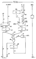
Cauchy cell 22 of Fig. 3 is illustrated in greater detail in Figs. 6a - 6c. Referring to Fig. 6a, the UC input of theCauchy cell 22 is applied to the 0 input of amultiplexer 50, whose output is applied to an m-bit A register 52. The output of theA register 52 is applied to one input of aGalois field multiplier 54. Parameters xi and yj (whose derivation is illustrated in Fig. 6b) are added together in an adder, namely an m-bit exclusive ORgate 56, whose output is applied to aninverting device 58 which forms the Galois field reciprocal of its input and applies this result to the 0 input of amultiplexer 60. (More complex Galois field inverters are disclosed in Berlekamp, Algebraic Coding Theory, Academic Press, 1968, pp. 36-44.) - The 1 input of the
multiplexer 60 receives the constant dj from aD register 62 whose contents is programmed in accordance with equation 5 (where j is the number of theCauchy cell 22 in the systolic array of Fig. 2). The value of dj is loaded into theD register 62 during system initialization and remains constant during operation. The output of themultiplexer 60 is applied to aB register 64, whose output, in turn, is applied to the other input of theGalois field multiplier 54. The output of themultiplier 54 is applied to one input of aGalois field adder 66 whose output is stored in anaccumulator register 68. The output of theaccumulator register 68 is recirculated through an ANDgate 70 to the other input of theadder 66. Whenever the RCTL signal (Fig. 7f) is zero, the ANDgate 70 causes the content of theaccumulator register 68 to be reset to zero in preparation for the next block of K message symbols. - As shown in Fig. 6a, the
quantity 1/(xi+yj) is present at the 0 input of themultiplexer 60, the quantity dj is present at the 1 input of themultiplexer 60 and the quantity uici is present at the 0 input of themultiplexer 50. Here, it should be noted that the first cycle of the clock signal is the one in which u₁ is received at the U input. Thus, "the ith cycle" is well defined. The cycle repeats itself for every codeword. During the ith cycle of the clock signal, the product uici is received at the UC input of theCauchy cell 22. (This is only true until i exceeds K, after which no more message symbols ui are received.) Simultaneously, the ASEL and BSEL control signals (Fig. 7c) are low, causing the uici and 1/(xi+yj) quantities to be multiplied together in themultiplier 54. The resulting product is added to the accumulated sum of previous such multiplications by theadder 66, the final accumulated sum being stored in theaccumulator register 68. Thus, at the end of K cycles of the clock signal, the quantity
1≦j≦R is stored in theaccumulator register 68. This quantity must be multiplied by dj in order to obtain the wj of equation (1). - At this point, the ASEL and BSEL control signals (Fig. 7c) become logic ones so that the quantity dj is applied by the
multiplexer 60 to one input of themultiplier 54 while the accumulated sum present at the input of theaccumulator 68 is applied by themultiplexer 50 to the other input of themultiplier 54 in order to perform the requisite multiplication by dj. After one more clock cycle, the computation of wj is complete. - After that, the control signal RCTL (Fig. 7f) controlling the AND
gate 70 becomes alogic 0 so that the ANDgate 70 applies a zero to one input of theadder 66. Then, wj (now present at the output of the multiplier 54) is added to zero by theadder 70 and applied to anRP output 72 of the Cauchy cell subsystem of Fig. 6a. TheRP output 72 is connected to the sub-system of Fig. 6c, discussed below. - Referring to the subsystem of Fig. 6b, the xi input to the subsystem of Fig. 6a is furnished from an
X register 74 whose contents is determined for each value of i (number of clock cycles) in accordance with equation (2). For this purpose, amultiplexer 76 receives the initial value x₁ at its 0 input from aregister 78 storing x₁. x₁ is the reciprocal of α, namely α⁻¹. (As mentioned earlier, α is simply a primitive element of the Galois field GF(2m)). The value of α⁻¹ is loaded into theregister 78 during system initialization and remains constant during operation. - The output of the
X register 74 is recirculated to aconstant multiplier 80 which multiplies the X register output by α⁻¹ and furnishes the resulting product to the 1 input of themultiplexer 76. - In operation, the XSEL control signal (Fig. 7e) is in the 0 state just before the arrival at cell j of the stream of K message symbols ui. At this point, the initial value x₁, namely α⁻¹, is loaded through the
multiplexer 76 into theX register 74. Then, the XSEL signal enters the 1 state and, in synchronism with the clock signal CK, the contents of theX register 74 is recirculated so as to be repeatedly multiplied by α⁻¹, so that it becomes α⁻², α⁻³ ... α-i (during the ith cycle of the clock signal)... etc... During the ith cycle of the clock signal, xi is present at the output of theregister 74 and is applied to the xi input of the adder 56 (Fig. 6a). - One implementation of the
constant multiplier 80 is shown in exploded view in Fig. 6b, for the three-bit example of GF(2³). In this example, all symbols are 3-bit binary numbers and theconstant multiplier 80 performs a linear transformation on each 3-bit byte applied at its X input to produce a 3-bit product byte at its Z output equal to X multiplied by α⁻¹. The linear transformation is indicated in Fig. 6b and need not be elaborated here. - The yj input to the
adder 56 of Fig. 6a is simply taken from a Yj register 82 whose contents is predetermined in accordance with equation (3), where j equals the number of theparticular cell 22 in the systolic array of Fig. 2. The value of yj is loaded into theregister 82 during system initialization and remains constant during system operation. - The jth Cauchy cell 22 (Fig. 2) is responsible for inserting the computed check symbol wj following the message stream emanating from the upstream neighboring cell (the j-1st cell). Fig. 6c illustrates the U input of the jth cell 22 and the U output of the same cell through which the message stream flows and where the check symbol wj must be inserted at the proper moment. A three-
input multiplexer 90 receives the message stream at its D1 input through an m-bit delay stage 92 (having a delay of one clock cycle) and at its D1P input (with no delay). The RP input of themultiplexer 90 is connected to theRP output 72 of the subsystem of Fig. 6a to receive the check symbol wj (to facilitate the injection of wj following the message stream at the proper moment). Themultiplexer 90 is controlled by a three-state logic signal OSEL (Fig. 7d). The output of the multiplexer 90 passes through another m-bit delay stage 94 before reaching the U output of thecell 22. - Referring to Fig. 7d, during the reception of the stream of the K message symbols ui, the OSEL signal is in its D1P state, so that the
multiplexer 90 receives, without any delay, each of the ui message symbols from the U input and sends them directly through thedelay 94 to the U output. In this state, the cell is transparent to (does not delay) the message/check symbol stream. Then, (in one embodiment of the present invention) following the conclusion of the message stream (after the last message symbol uk has been received), the OSEL signal changes to its RP state. This causes the check byte wj present at theRP output 72 of the jth cell 22 (subsystem of Fig. 6a) to be loaded through the RP input of themultiplexer 90 and sent through thedelay 94 to the U output of the cell 22 (subsystem of Fig. 6c). In the meantime, the check symbol wj-1 (and its predecessors), which had (up to this point) immediately followed the last message symbol uk, is being held (for one clock cycle) in thedelay stage 92. At the end of this cycle, the OSEL signal leaves its RP state and enters its D1 state. Thus, the check symbol wj-1 held in the delay stage 92 (and all subsequent check symbols) is now transmitted by themultiplexer 90 from its D1 input through thedelay stage 94 to the U output immediately following the last check symbol wj previously furnished through the RP input of themultiplexer 90. Thus, the subsystem of Fig. 6c, in effect, creates a gap between the incoming message stream and the trailing stream of check symbols and inserts the check symbol computed in the present cell into the gap. - If the number K of redundant characters is to be reduced to R-1, then the last cell (cell R) in the array of Fig. 2 is "disabled" by preventing its OSEL signal from ever leaving the D1P ("transparent") state. More cells may be so disabled for further reductions in R. To increase R, selected ones of the disabled cells may be enabled, as desired.
- In an alternative embodiment, the check symbol wj is inserted at the end of the check byte stream (i.e. after wj+1) (rather than being inserted between the message stream and the trailing check byte stream), so as to insert the R check symbols wj into the stream in the opposite order from that described above. This feature requires more complex control.
- In an alternative embodiment, ci and dj may be set to 1 for each 1≦i≦K, 1≦j≦R (thus, in effect, dispensing with the multiplications by these parameters). Actually, this significantly simplifies the system: it eliminates the uici processor altogether, as well as the need for separate ui and uici inputs/outputs. In this alternative embodiment, the encoder would append to the message stream R check symbols computed (as a result of this modification) in accordance with a "generalized Reed-Solomon Code" of the type described, for example, in the above-referenced publication by Seroussi and Roth.
- The control signals ASEL, BSEL, OSEL, XSEL and RCTL discussed previously in connection with Fig. 6a, b and c and Figs. 7a, b, c, d, e and f are generated in synchronism with the clock signal CK within each cell by the
control logic circuit 96 which receives the SMCi and CK signals from the SMC and CK_IN inputs of thecell 22. The control logic circuit distributes a version of the clock signal CK to all of the registers in thecell 22. A skilled worker may readily implement thecontrol logic circuit 96 as a programmable logic array (or the like) in accordance with Figs. 7a-7f. - Fig. 6c illustrates the "CK_IN" clock input to the cell, receiving the clock signal CK from the neighboring upstream cell. The
control logic circuit 96 receives the clock signal CK from the CK_IN input and passes it on to the clock output CK_OUT output of the cell to the neighboring downstream cell. Cell operation timing, controlled by thelogic circuit 96, is therefore synchronous only between adjacent cells, and is otherwise asynchronous. The advantage is that the longest clock delay is the short distance between adjacent cells, and the system may therefore operate at very fast clock rates.
Claims (6)
- A systolic systematic Reed-Solomon encoder for encoding a stream of K message symbols, said encoder having a plurality of R identical successive cells (22) connected in series, whereby said stream of message symbols may flow through said series of cells (22) so that each cell receives a current message symbol from its upstream neighbor cell while transmitting the previous message symbol to its downstream neighbor cell and each of said cells (22) comprises means for performing at least a portion of a Galois Field Arithmetic computation of a corresponding redundant check symbol wj according to the formula:

a common processor (20) adapted to perform the calculation of at least the product ui·ci of said Galois Field computation once to generate a partial result, whereby said partial result is made available successively to each of said R successive cells (22). - The encoder of Claim 1 wherein said identical successive cells (22) are of the type that is known as Cauchy cell.
- The encoder of Claims 1 or 2 wherein said encoder is adapted to process a stream of K message symbols ui, where the index i runs from 1 through K,
wherein each of said cells (22) computes an individual one of R redundant check symbols, said common processor (20) comprising:
means (30) for storing a first constant c₁;
means (37) for supplying a recursion ratio ci+1/ci for each index i;
means (34) for multiplying a given constant ci by said ratio to determine the next constant ci+1 and
means (42) for computing the product between each message symbol ui and the corresponding constant ci. - The encoder of Claim 3 wherein said processor (20) comprises means for providing said value ui·ci for said successive cells (22) for computing said redundant check symbols by said cells (22).
- A method for systematically systolically encoding a stream of K message symbols ui, where the index i runs from 1 through K, in accordance with a Reed-Solomon code generator polynomial, by performing in each of a plurality of R identical successive cells (22) at least a portion of a Galois Field Arithmetic computation of a corresponding redundant check symbol wj according to the formula:

characterized by:
a process common for all of said successive cells (22) for computing a product ui·ci, whereby this product is provided successively to each of said successive cells (22). - The method of claim 5, said common process comprising the following steps:
storing a fixed constant c₁;
storing a recursion ratio ci + 1/ci for each value of said index i;
multiplying each ci with each of said message symbols ui for each value of said index i.
Applications Claiming Priority (3)
| Application Number | Priority Date | Filing Date | Title |
|---|---|---|---|
| US07/107,207 US4835775A (en) | 1987-10-13 | 1987-10-13 | Hypersystolic reed-solomon encoder |
| US107207 | 1987-10-13 | ||
| PCT/US1988/003382 WO1989003621A1 (en) | 1987-10-13 | 1988-10-05 | Hypersystolic reed-solomon encoder |
Publications (2)
| Publication Number | Publication Date |
|---|---|
| EP0393080A1 EP0393080A1 (en) | 1990-10-24 |
| EP0393080B1 true EP0393080B1 (en) | 1994-12-28 |
Family
ID=22315424
Family Applications (1)
| Application Number | Title | Priority Date | Filing Date |
|---|---|---|---|
| EP88909680A Expired - Lifetime EP0393080B1 (en) | 1987-10-13 | 1988-10-05 | Hypersystolic reed-solomon encoder |
Country Status (4)
| Country | Link |
|---|---|
| US (1) | US4835775A (en) |
| EP (1) | EP0393080B1 (en) |
| DE (1) | DE3852648T2 (en) |
| WO (1) | WO1989003621A1 (en) |
Families Citing this family (14)
| Publication number | Priority date | Publication date | Assignee | Title |
|---|---|---|---|---|
| US4996690A (en) * | 1988-08-26 | 1991-02-26 | Stac Electronics | Write operation with gating capability |
| US5130990A (en) * | 1990-02-15 | 1992-07-14 | The United States Of America, As Represented By The Administrator, National Aeronautics And Space Administration | VLSI architecture for a Reed-Solomon decoder |
| US5115436A (en) * | 1990-05-04 | 1992-05-19 | Bell Communications Research | Forward error correction code system |
| US5659780A (en) * | 1994-02-24 | 1997-08-19 | Wu; Chen-Mie | Pipelined SIMD-systolic array processor and methods thereof |
| US5761220A (en) * | 1994-09-19 | 1998-06-02 | Cirrus Logic, Inc. | Minimum latency asynchronous data path controller in a digital recording system |
| US5553272A (en) * | 1994-09-30 | 1996-09-03 | The University Of South Florida | VLSI circuit structure for determining the edit distance between strings |
| US5778009A (en) * | 1995-06-14 | 1998-07-07 | Quantum Corporation | Dedicated ALU architecture for 10-bit Reed-Solomon error correction module |
| US6405339B1 (en) * | 1999-08-31 | 2002-06-11 | International Business Machines Corporation | Parallelized programmable encoder/syndrome generator |
| AU1691101A (en) * | 1999-09-25 | 2001-04-30 | Manfred Rieck | Method and devices for production of a digital code for correction of transmission errors and error correcting decoding thereof |
| US6738942B1 (en) | 2000-06-02 | 2004-05-18 | Vitesse Semiconductor Corporation | Product code based forward error correction system |
| US6694476B1 (en) | 2000-06-02 | 2004-02-17 | Vitesse Semiconductor Corporation | Reed-solomon encoder and decoder |
| US8707143B1 (en) * | 2011-06-13 | 2014-04-22 | Altera Corporation | Multiplication-based reed-solomon encoding architecture |
| US10445323B2 (en) * | 2015-09-30 | 2019-10-15 | University Of Virginia Patent Foundation | Association rule mining with the micron automata processor |
| US10181864B2 (en) | 2016-02-26 | 2019-01-15 | Altera Corporation | Methods and apparatus for performing reed-solomon encoding |
Family Cites Families (3)
| Publication number | Priority date | Publication date | Assignee | Title |
|---|---|---|---|---|
| US4584686A (en) * | 1983-12-22 | 1986-04-22 | Optical Storage International | Reed-Solomon error correction apparatus |
| US4665523A (en) * | 1984-02-15 | 1987-05-12 | Stanford University | Method and means for error detection and correction in high speed data transmission codes |
| US4747103A (en) * | 1985-03-21 | 1988-05-24 | Canon Kabushiki Kaisha | Signal processing apparatus for correcting decoding errors |
-
1987
- 1987-10-13 US US07/107,207 patent/US4835775A/en not_active Expired - Fee Related
-
1988
- 1988-10-05 WO PCT/US1988/003382 patent/WO1989003621A1/en active IP Right Grant
- 1988-10-05 DE DE3852648T patent/DE3852648T2/en not_active Expired - Fee Related
- 1988-10-05 EP EP88909680A patent/EP0393080B1/en not_active Expired - Lifetime
Non-Patent Citations (3)
| Title |
|---|
| IEEE Transactions on Computers, vol.C-34, no.5, May 1985, IEEE; H.M.Shao et al: "A VLSI design of a pipeline Reed-Solomon decoder", pages 393-403 * |
| IEEE Transactions on Information Theory, vol.IT-31, no.6, November 1985, IEEE, R.M.Roth et al: "On generator matrices of MDS codes", pages 826-830 * |
| NTIS Technical Notes, no.4, part B, April 1986 (Springfield, Virginia US) "Systolic VLSI Reed-Solomon decoder", page 403 * |
Also Published As
| Publication number | Publication date |
|---|---|
| DE3852648D1 (en) | 1995-02-09 |
| US4835775A (en) | 1989-05-30 |
| EP0393080A1 (en) | 1990-10-24 |
| DE3852648T2 (en) | 1995-08-17 |
| WO1989003621A1 (en) | 1989-04-20 |
Similar Documents
| Publication | Publication Date | Title |
|---|---|---|
| US5440570A (en) | Real-time binary BCH decoder | |
| EP0114938B1 (en) | On-the-fly multibyte error correction | |
| EP0158510B1 (en) | Error detection and correction in digital communication systems | |
| EP0393080B1 (en) | Hypersystolic reed-solomon encoder | |
| US6347389B1 (en) | Pipelined high speed reed-solomon error/erasure decoder | |
| JP3046988B2 (en) | Method and apparatus for detecting frame synchronization of data stream | |
| US5805617A (en) | Apparatus for computing error correction syndromes | |
| KR100309724B1 (en) | Reed solomon coding apparatus and reed solomon coding method | |
| US4312069A (en) | Serial encoding-decoding for cyclic block codes | |
| KR890004677B1 (en) | Decoding method and apparatus for cyclic codes | |
| EP0249982B1 (en) | Decoder | |
| CN112468161A (en) | RS high-speed coding circuit | |
| KR19990016134A (en) | High Speed Serial Error Position Polynomial Computation Circuit | |
| JPH0575479A (en) | Circuit apparatus for identifying, revising and correcting error in data flow | |
| EP0720759B1 (en) | Programmable redundancy/syndrome generator | |
| US4488302A (en) | Burst error correction using cyclic block codes | |
| EP0660535B1 (en) | Apparatus for uniformly correcting erasure and error of received word by using a common polynomial | |
| US6219816B1 (en) | Device and method for carrying out Reed-Solomon encoding | |
| EP0991196B1 (en) | Method of correcting lost data and circuit thereof | |
| US6859905B2 (en) | Parallel processing Reed-Solomon encoding circuit and method | |
| EP0584864B1 (en) | A hardware-efficient method and device for encoding BCH codes and in particular Reed-Solomon codes | |
| EP0341851A2 (en) | Method and apparatus for interleaved encoding | |
| JP2710176B2 (en) | Error position and error pattern derivation circuit | |
| SU1018119A1 (en) | Mass storage error protection device | |
| JPH06290065A (en) | Euclidean algorithm circuit |
Legal Events
| Date | Code | Title | Description |
|---|---|---|---|
| PUAI | Public reference made under article 153(3) epc to a published international application that has entered the european phase |
Free format text: ORIGINAL CODE: 0009012 |
|
| 17P | Request for examination filed |
Effective date: 19900410 |
|
| AK | Designated contracting states |
Kind code of ref document: A1 Designated state(s): DE FR GB NL |
|
| 17Q | First examination report despatched |
Effective date: 19930115 |
|
| RBV | Designated contracting states (corrected) |
Designated state(s): DE FR GB |
|
| GRAA | (expected) grant |
Free format text: ORIGINAL CODE: 0009210 |
|
| REF | Corresponds to: |
Ref document number: 3852648 Country of ref document: DE Date of ref document: 19950209 |
|
| ET | Fr: translation filed | ||
| PG25 | Lapsed in a contracting state [announced via postgrant information from national office to epo] |
Ref country code: GB Effective date: 19951005 |
|
| PLBE | No opposition filed within time limit |
Free format text: ORIGINAL CODE: 0009261 |
|
| STAA | Information on the status of an ep patent application or granted ep patent |
Free format text: STATUS: NO OPPOSITION FILED WITHIN TIME LIMIT |
|
| 26N | No opposition filed | ||
| GBPC | Gb: european patent ceased through non-payment of renewal fee |
Effective date: 19951005 |
|
| PG25 | Lapsed in a contracting state [announced via postgrant information from national office to epo] |
Ref country code: FR Effective date: 19960628 |
|
| PG25 | Lapsed in a contracting state [announced via postgrant information from national office to epo] |
Ref country code: DE Effective date: 19960702 |
|
| REG | Reference to a national code |
Ref country code: FR Ref legal event code: ST |