EP0389584B1 - Transistor breakdown protection circuit - Google Patents
Transistor breakdown protection circuit Download PDFInfo
- Publication number
- EP0389584B1 EP0389584B1 EP89909179A EP89909179A EP0389584B1 EP 0389584 B1 EP0389584 B1 EP 0389584B1 EP 89909179 A EP89909179 A EP 89909179A EP 89909179 A EP89909179 A EP 89909179A EP 0389584 B1 EP0389584 B1 EP 0389584B1
- Authority
- EP
- European Patent Office
- Prior art keywords
- protecting
- transistors
- coupled
- protection circuit
- fets
- Prior art date
- Legal status (The legal status is an assumption and is not a legal conclusion. Google has not performed a legal analysis and makes no representation as to the accuracy of the status listed.)
- Expired - Lifetime
Links
Images
Classifications
-
- H—ELECTRICITY
- H03—ELECTRONIC CIRCUITRY
- H03K—PULSE TECHNIQUE
- H03K17/00—Electronic switching or gating, i.e. not by contact-making and –breaking
- H03K17/08—Modifications for protecting switching circuit against overcurrent or overvoltage
- H03K17/081—Modifications for protecting switching circuit against overcurrent or overvoltage without feedback from the output circuit to the control circuit
- H03K17/0814—Modifications for protecting switching circuit against overcurrent or overvoltage without feedback from the output circuit to the control circuit by measures taken in the output circuit
- H03K17/08142—Modifications for protecting switching circuit against overcurrent or overvoltage without feedback from the output circuit to the control circuit by measures taken in the output circuit in field-effect transistor switches
-
- G—PHYSICS
- G11—INFORMATION STORAGE
- G11C—STATIC STORES
- G11C16/00—Erasable programmable read-only memories
- G11C16/02—Erasable programmable read-only memories electrically programmable
- G11C16/06—Auxiliary circuits, e.g. for writing into memory
- G11C16/10—Programming or data input circuits
- G11C16/12—Programming voltage switching circuits
-
- G—PHYSICS
- G11—INFORMATION STORAGE
- G11C—STATIC STORES
- G11C16/00—Erasable programmable read-only memories
- G11C16/02—Erasable programmable read-only memories electrically programmable
- G11C16/06—Auxiliary circuits, e.g. for writing into memory
- G11C16/22—Safety or protection circuits preventing unauthorised or accidental access to memory cells
- G11C16/225—Preventing erasure, programming or reading when power supply voltages are outside the required ranges
-
- H—ELECTRICITY
- H03—ELECTRONIC CIRCUITRY
- H03K—PULSE TECHNIQUE
- H03K17/00—Electronic switching or gating, i.e. not by contact-making and –breaking
- H03K17/10—Modifications for increasing the maximum permissible switched voltage
- H03K17/102—Modifications for increasing the maximum permissible switched voltage in field-effect transistor switches
-
- H—ELECTRICITY
- H03—ELECTRONIC CIRCUITRY
- H03K—PULSE TECHNIQUE
- H03K17/00—Electronic switching or gating, i.e. not by contact-making and –breaking
- H03K17/51—Electronic switching or gating, i.e. not by contact-making and –breaking characterised by the components used
- H03K17/56—Electronic switching or gating, i.e. not by contact-making and –breaking characterised by the components used by the use, as active elements, of semiconductor devices
- H03K17/687—Electronic switching or gating, i.e. not by contact-making and –breaking characterised by the components used by the use, as active elements, of semiconductor devices the devices being field-effect transistors
- H03K17/693—Switching arrangements with several input- or output-terminals, e.g. multiplexers, distributors
-
- H—ELECTRICITY
- H03—ELECTRONIC CIRCUITRY
- H03K—PULSE TECHNIQUE
- H03K19/00—Logic circuits, i.e. having at least two inputs acting on one output; Inverting circuits
- H03K19/003—Modifications for increasing the reliability for protection
- H03K19/00315—Modifications for increasing the reliability for protection in field-effect transistor circuits
Definitions
- This invention relates to transistor breakdown protection circuits for use in high voltage circuitry.
- This inventions relates more particularly to memory systems such as Electrically Erasable Programmable Read Only Memory (EEPROM), or Non-Volatile Random Access Memory (NVRAM) which require high voltages for write and erase operations.
- EEPROM Electrically Erasable Programmable Read Only Memory
- NVRAM Non-Volatile Random Access Memory
- protecting transistors are provided in connection with the buffer gates.
- the protecting transistors are only useful during the write/erase operation and at all other times the voltage applied to the protecting transistors' gates are selected so that the protecting transistors are switched "on" so as not to disturb the logic function of the memory system.
- Such an arrangement is used in the MC68HC11 EEPROM write amplifier supplied by Motorola Inc. which is also designed so that it can operate with a three state function output.
- the tristate function is realised by a transmission gate able to support high voltage and which is coupled to the buffer gates.
- the transmission gate is made up of four coupled transistors. Since the buffer and transmission gate are connected to each column of the EEPROM memory a large number of transistors are required to create a tristate function resulting in greater circuit size and cost.
- Non-Volatile RAM NVRAM
- Applicant's UK patent application No. 8702785
- NVRAM Non-Volatile RAM
- a high voltage for write/erase operation is required.
- the above referred to UK application discloses presetting the memory cells by using a single pull-down transistor per column. However, a very large transistor is required to pull-down all the RAM cells on the same column which can create significant power consumption and can make the preset difficult.
- a high voltage transistor breakdown protection circuit for protecting transistor circuitry when a high voltage is supplied thereto, the transistor circuitry comprising first and second transistors coupled in series between a supply line and a reference line, the protection circuit comprising: protecting means having a first input and a second input, the protecting means comprising first and second protecting transistors coupled in series between the first and second transistors to form an inverter, the control electrode of the first protecting transistor being coupled to the first input and the control electrode of the second protecting transistor being coupled to the second input, a connection node between the first and second protecting transistors being coupled to an output of the transistor circuitry; protection control means coupled to said first and second inputs of said protecting means to apply first and second signals thereto, each of said first and second protecting transistors being switched on or off depending on which of the first and second signals is applied to the first and second inputs respectively, said protecting means assuming, in dependence on said protection control means applying to said first and second inputs first and second combinations of said first and second signals, a protecting mode when the
- the write amplifier 2 has a plurality of inverters, only one of which 4 is shown, such that each inverter 4 is connected to one row of cells in a single plane of EEPROM memory (not shown).
- the inverter 4 comprises a transmission gate 6, which is made up of four field effect transistors (FET) 10, 12, 14, 16 and a group of four transistors 18, 20, 22, 24 coupled in series, comprising two buffer gates 18, 24 and two protection transistors 20, 22.
- Two voltage supply lines HVPP and HVPN connected to the gates of the protecting transistors 20 and 22 respectively, control the "on/off" state of the protecting transistors.
- the gate electrodes of the buffer gates 18, 24 are coupled to form the input of the inverter 4 and the second electrodes of the FETs 14, 16 of the transmission gate are coupled to form the output of the inverter 4.
- a high voltage is supplied to the write amplifier 2 from a supply line (usually at voltage V DD ) pulled to the programming voltage V PP .
- the lines HVPP and HVPN are pulled high so that a voltage V HN is applied to the gates of the protecting transistors 20 and 22.
- V SS voltage
- protecting transistor 20 is switched “on” and protecting transistor 22 provides protection against breakdown in the buffer transistor 24.
- protecting transistor 22 is switched “on” and protecting transistor 20 provides protection against breakdown in the buffer transistor 18.
- the supply line is pulled to the lower voltage V DD and in order that the protecting transistors 20, 22 do not disturb the logic function of the inverter 4, the HVPN line is held at the potential V HN so that the protecting transistor 22 is "on” and the HVPP line is pulled to the potential V SS so that the protecting transistor 20 is switched “on”.
- a three state output such as in the MC68HC11 EEPROM write amplifier supplied by Motorola Inc, is generated by the transmission gate 6 whose state is controlled by a driver 8.
- a high voltage is applied to the gates of two of the FETs 12, 16.
- Such a write amplifier is well known in the art.
- the write amplifier 28 of Figure 2 has a command block 34 and a plurality of inverters, only one of which 40 is shown, such that each inverter is associated with one row of cells in a plane of EEPROM memory (not shown).
- the inverters are supplied from a common supply line (normally at voltage V DD ) and a line at datum potential V SS .
- the inverter 40 includes four FET transistors 29, 30, 32, 33 coupled together in series by their current electrodes.
- the first and second transistors are p-channel FETs, the third and fourth are n-channel FETs.
- the gate electrodes of the first and fourth FETs 29, 33 form the input of the inverter 40 and the second current electrodes of the second and third FETs 30, 32 are coupled to form the output of the inverter 40.
- the first current electrode of the first FET 29 is coupled to the supply line and also to the bulk electrode of the second FET 30, and the bulk electrode of the first FET 29 is also tied to this first current electrode.
- the fourth FET 33 is connected to the line at datum potential V SS .
- the gate electrodes of the second and third FETs 30, 32 are coupled to the command block 34 by two voltage lines 36, 38 respectively.
- the command block 34 can control whether these FETs 30 and 32 act as protection transistors when the supply voltage is V PP or are used to create the tristate function when the supply voltage is V DD .
- the command block 34 includes four switching transistors 42, 44. 52, 54 and four command transistors 56, 58, 60, 62-
- the voltage line 36 is connected to the HVPP line via the first and second switching transistors 42, 44 coupled in parallel.
- the first current electrode of the first switching transistor 42 is connected together with the second current electrode of the second switching transistor 44 to the voltage line 36, and the second current electrode of the first switching transistor 42 is connected together with the first current electrode of the second switching transistor 44 to the HVPP line.
- the first switching transistor 42 is a n-channel FET whose gate electrode is connected to a fourth common voltage line 46.
- the second switching transistor 44 is a p-channel FET, whose gate electrode is connected to a third common voltage line 48 and whose bulk electrode is connected to a first common voltage line 50.
- the first common voltage line 50 is connected to the HVPN line.
- the voltage line 38 is connected to the HVPN line and the first common voltage line 50 via the third and fourth switching transistors 52, 54 coupled in parallel in an identical way to that described above for the voltage line 36.
- the third switching transistor 52 is a n-channel FET and the fourth switching transistor 54 is a p-channel FET.
- the first and third command transistors 56, 60 are coupled together in series by way of the current electrodes as are the second and fourth command transistors 58, 62.
- the first and second command transistors 56, 58 are p-channel enhancement FETs, whose gate electrodes are cross-coupled respectively to the second and first nodes D and B located between the first current electrodes of the fourth and third command transistors 62, 60 respectively.
- the nodes B and D are connected respectively to the third and fourth common voltage lines 48, 46.
- the first current electrodes of the first and second command FETs 56, 58 are coupled to the first common voltage line 50 for receiving a voltage supply from the HVPN line and these first current electrodes are also connected to their respective bulk electrodes.
- the third and fourth command transistors are n-channel FET whose gates are coupled to tristate command lines 64, 66 respectively for receiving mode command signals and whose second current electrodes are both connected to a second common voltage line 68 at datum potential V SS .
- the first common voltage line 50 is coupled to the voltage line 36 via the first current electrode of a p-channel enhancement FET 70 whose gate electrode is connected to the fourth common voltage line 46 and whose bulk electrode is connected to the first current electrode.
- the second common voltage line 68 at voltage V SS is coupled to the voltage line 38 via the second current electrode of a n-channel FET 72 whose gate electrode is connected to the third common voltage line 48.
- a high programming voltage V PP is supplied from the supply line to the inverter 40 and in order to protect against breakdown in the buffer transistors 29, 33, which may occur when the voltage applied to the input of the inverter 40 is high, V DD , and low, V SS , respectively, the voltages on both the HVPP and HVPN lines are pulled up to a voltage V HN .
- a voltage V HN is therefore applied to the gate electrodes of the intermediate FETs 30, 32, via the switching transistors 42, 44 and 52, 54 respectively, so that when the voltage applied to the input of the inverter 40 is low, V SS , the FET 30 is switched “on” and FET 32 provides protection whereby the voltage applied to the buffer transistor 33 is prevented from reaching the breakdown voltage limit.
- V DD When the voltage applied to the input of the inverter 40 is high, V DD , the FET 32 is switched “on” and the FET 30 provides protection whereby the voltage applied to the buffer transistor 29 is prevented from reaching the breakdown voltage limit. In both cases the limit is dependent on the particular transistors utilised.
- V DD When a write operation is not being performed a low voltage V DD is supplied from the supply line and by controlling the voltages on the HVPP and HVPN lines by way of the four command transistors 56, 58, 60, 62 which are in turn controlled by the tristate command lines 64, 66 the intermediate FETs 30, 32 can be switched “on” or “off” thereby creating the tristate function. Therefore, when the supply line is at potential V DD the output from the inverter 40 can be one of three possible states: binary '1' (potential V DD ), binary '0' (potential V SS ) and floating.
- the static RAM cell 74 which is one cell of an array of identical cells of the RAM structure which forms part of a NVRAM memory system, includes two FETs 76, 78 having their current electrodes coupled in series between a pair of split column select lines C, CN.
- the gate electrodes of the FETs 76, 78 are connected to a row select line R, and an inverting buffer amplifier arrangement A is connected between the FETs 76, 78 and supplied from a supply line (normally at voltage V DD ) and a line a datum potential V SS .
- a supply line normally at voltage V DD
- V SS datum potential
- the inverting buffer amplifier arrangement A includes p-channel FETs 80, 82 and n-channel FETs 84, 86 which protect the buffer transistors 88, 90, 92, 94 against voltage breakdown.
- the gates of the p-channel protection transistors 80, 82 are coupled to a voltage line HVPP and the gates of the n-channel protection transistors 84, 86 are coupled to a voltage line HVPN.
- protecting transistors 82 and 86 are switched “on” and protecting transistors 80 and 84 provide protection against breakdown in the buffer transistors 88 and 94.
- protecting transistors 82 and 86 provide protection against breakdown in the buffer transistors 90 and 92.
- the RAM cells 74 are preset by using a single pull down per column to a voltage V SS via a transistor 96 on each cell's column select line CN. However, pulling down all the cells on the same column creates difficulty in performing the preset and since a large transistor must be used in order to turn the RAM cells, significant power consumption results.
- the RAM cell 98 includes a RAM cell of the same structure as shown in Figure 3, but wherein the gate electrodes of the p- and n-channel protecting transistors 82, 80 and 84, 86 are coupled respectively by two voltage lines 126, 128 to the HVPP and the HVPN lines via a command block 100. As shown, like components to those of Figure 3 are referenced by the same numerals.
- the voltages applied to the gates of the p-channel protecting transistors 80, 82 and n-channel protecting transistors 84, 86 are controlled by the command block 100.
- the command block 100 is similar to that of the command block 34 of the write amplifier 28 in Figure 2 in that there are four command transistors 102, 104, 106, 108 interconnected identically to the command transistors 56, 58, 60, 62 of the write amplifier, and four common voltage lines 114, 116, 112, 110.
- the second common voltage line 116 at datum potential V SS is coupled to the datum potential line of the RAM cell 99.
- only the state of the p-channel protecting transistors 82, 80 need be controlled.
- the command block 100 has only two switching transistors 118, 120 coupled between the HVPP line and the voltage line 126 to control the voltage applied to the p-channel protecting transistors 80, 82.
- the HVPN line connects to the voltage line 128 by way of the first common voltage line 114.
- the command transistors 102, 104, 106, 108 are controlled by the voltage on two pull-up inhibit lines 122, 124 applied to the gate electrodes of the command transistors 106, 108 and this allows for the disabling of the p-channel protection transistors 80, 82.
- V DD When a high voltage, V DD , is applied to node Y the protecting transistors 80 and 84 are switched “on" and 82 and 86 provide protection whereby the voltages applied to the buffer transistors 90 and 92 are respectively prevented from reaching the breakdown voltage limit.
- the RAM cells 99 Before program and/or data can be transferred to the RAM array of the NVRAM memory system (not shown), the RAM cells 99 must be preset via a transistor 96 on each cell's column select line CN. During preset activation, the voltage supply line is at a voltage V DD and the voltage supplied to the gate electrodes of the p-channel protecting transistors 80, 82, which is controlled by the pull-up inhibit lines 122, 124, is pulled to V HN switching the p-channel protecting transistors 80, 82 "off".
- the column select line CN of a column of RAM cells 99 in the array can be pulled down by one transistor 96 to a potential V SS thereby making the preset easier and also with reduced power consumption since a smaller transistor can be used.
- the pull-up inhibit of the p-channel protecting transistors is then deselected by controlling the voltage on the pull-up inhibit lines 122, 124, which restores the flip-flop function of the RAM cell.
- transistors fabricated in N-well technology have been utilised, wherein, p-channel transistors are represented with four electrodes and n-channel transistors with three electrodes.
- p-channel transistor the bulk electrode connection is explicitly drawn so as to indicate at which potential the channel is connected.
- this connection need not be shown as the n-channel transistors are implemented directly in the substrate which is tied to the ground voltage.
Landscapes
- Engineering & Computer Science (AREA)
- Computer Security & Cryptography (AREA)
- Computer Hardware Design (AREA)
- Computing Systems (AREA)
- General Engineering & Computer Science (AREA)
- Mathematical Physics (AREA)
- Physics & Mathematics (AREA)
- Static Random-Access Memory (AREA)
- Read Only Memory (AREA)
- Electronic Switches (AREA)
- Dram (AREA)
- Semiconductor Memories (AREA)
- Storage Device Security (AREA)
Abstract
Description
- This invention relates to transistor breakdown protection circuits for use in high voltage circuitry. This inventions relates more particularly to memory systems such as Electrically Erasable Programmable Read Only Memory (EEPROM), or Non-Volatile Random Access Memory (NVRAM) which require high voltages for write and erase operations.
- In memory systems such as EEPROM or NVRAM, to transfer program and/or data a high voltage is required to write to or erase the memory cells and therefore, to avoid voltage breakdown in the buffer transistors of the memory cells at high voltages, protecting transistors are provided in connection with the buffer gates. The protecting transistors are only useful during the write/erase operation and at all other times the voltage applied to the protecting transistors' gates are selected so that the protecting transistors are switched "on" so as not to disturb the logic function of the memory system.
- Such an arrangement is used in the MC68HC11 EEPROM write amplifier supplied by Motorola Inc. which is also designed so that it can operate with a three state function output. The tristate function is realised by a transmission gate able to support high voltage and which is coupled to the buffer gates. The transmission gate is made up of four coupled transistors. Since the buffer and transmission gate are connected to each column of the EEPROM memory a large number of transistors are required to create a tristate function resulting in greater circuit size and cost.
- A similar arrangement of buffer gates and protecting transistors is found in the RAM cells of Non-Volatile RAM (NVRAM) memory systems such as that described in Applicant's UK patent application (No. 8702785) entitled "Memory System". As with the above described write amplifier, in the memory system a high voltage for write/erase operation is required. However it is also important to perform a full preset of the entire RAM array before performing a recall. This can be achieved by individually pulling down each cell using a respective transistor, however this requires a large number of transistors. The above referred to UK application discloses presetting the memory cells by using a single pull-down transistor per column. However, a very large transistor is required to pull-down all the RAM cells on the same column which can create significant power consumption and can make the preset difficult.
- It is an object of the present invention to provide a high voltage transistor breakdown protection circuit for a memory system wherein the above disadvantages may be obviated.
- In accordance with the present invention there is provided a high voltage transistor breakdown protection circuit for protecting transistor circuitry when a high voltage is supplied thereto, the transistor circuitry comprising first and second transistors coupled in series between a supply line and a reference line, the protection circuit comprising:
protecting means having a first input and a second input, the protecting means comprising first and second protecting transistors coupled in series between the first and second transistors to form an inverter, the control electrode of the first protecting transistor being coupled to the first input and the control electrode of the second protecting transistor being coupled to the second input, a connection node between the first and second protecting transistors being coupled to an output of the transistor circuitry;
protection control means coupled to said first and second inputs of said protecting means to apply first and second signals thereto, each of said first and second protecting transistors being switched on or off depending on which of the first and second signals is applied to the first and second inputs respectively,
said protecting means assuming, in dependence on said protection control means applying to said first and second inputs first and second combinations of said first and second signals, a protecting mode when the high voltage is supplied to the supply line in which the first and second protection transistors protect the first and second transistors from voltage breakdown or a non-protecting mode when a low voltage is supplied to the supply line, the protection circuit being characterised by,
said protecting means being arranged to assume a third mode or a fourth mode when the low voltage is supplied to the first voltage supply line in dependence on said protection control means applying to said first and second inputs third and fourth combinations of said first and second signals whereby the non-protecting, third and fourth modes of the protecting means operate to provide different logic functions at the output of the transistor circuitry. - Thus, it will be appreciated that by replacing the transmission gate and the high voltage translator of the write amplifier by a circuit wherein the protection transistors are used both as protection against breakdown in the buffer transistors at high voltages and for creating the tristate function at low voltages, the number of transistors are reduced considerably, which reduces the circuit size and cost. Thus power consumption will be decreased and working safety improved.
- It will also be appreciated that by using such a protecting circuit arrangement in the RAM cell of a NVRAM memory system a tristate effect can be created into the RAM cell thereby making the preset easier since the pull-up action of the p transistors in the memory cell during preset activation can now be disabled. Thus a large transistor is not required thereby reducing the power consumption.
- Two memory systems in accordance with the present invention will now be described, by way of example only, with reference to the accompanying drawings, in which:
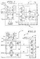
- Figure 1 is a schematic diagram showing the circuit of a write amplifier of a prior art memory system;
- Figure 2 is a schematic diagram showing the circuit of a write amplifier of a first memory system in accordance with the present invention;
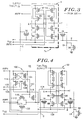
- Figure 3 is a schematic diagram showing the circuit of part of a prior art NVRAM memory system;
- Figure 4 is a schematic diagram showing the circuit of part of a second memory system in accordance with the present invention.
- Referring firstly to Figure 1, the
write amplifier 2 has a plurality of inverters, only one of which 4 is shown, such that eachinverter 4 is connected to one row of cells in a single plane of EEPROM memory (not shown). Theinverter 4 comprises a transmission gate 6, which is made up of four field effect transistors (FET) 10, 12, 14, 16 and a group of fourtransistors buffer gates protection transistors transistors buffer gates inverter 4 and the second electrodes of theFETs inverter 4. - In operation of the
write amplifier 2, for a write operation a high voltage is supplied to thewrite amplifier 2 from a supply line (usually at voltage VDD) pulled to the programming voltage VPP. The lines HVPP and HVPN are pulled high so that a voltage VHN is applied to the gates of the protectingtransistors inverter 4, protectingtransistor 20 is switched "on" and protectingtransistor 22 provides protection against breakdown in thebuffer transistor 24. When a high voltage VDD is applied to the input of theinverter 4, protectingtransistor 22 is switched "on" and protectingtransistor 20 provides protection against breakdown in thebuffer transistor 18. When a write operation is not being performed, the supply line is pulled to the lower voltage VDD and in order that the protectingtransistors inverter 4, the HVPN line is held at the potential VHN so that the protectingtransistor 22 is "on" and the HVPP line is pulled to the potential VSS so that the protectingtransistor 20 is switched "on". A three state output, such as in the MC68HC11 EEPROM write amplifier supplied by Motorola Inc, is generated by the transmission gate 6 whose state is controlled by adriver 8. Thus to command the transmission gate 6, a high voltage is applied to the gates of two of theFETs - Referring now to Figure 2, in order to reduce the number of transistors which are required for the write amplifier referred to above, while still providing protection against voltage breakdown at a high supply voltage VPP as well as providing a tristate function output at a lower supply voltage VDD, the two protection transistors are used to perform both functions. The manner in which this is achieved will be described fully below.
- In a preferred embodiment of the present invention the
write amplifier 28 of Figure 2 has acommand block 34 and a plurality of inverters, only one of which 40 is shown, such that each inverter is associated with one row of cells in a plane of EEPROM memory (not shown). The inverters are supplied from a common supply line (normally at voltage VDD) and a line at datum potential VSS. Theinverter 40 includes fourFET transistors fourth FETs inverter 40 and the second current electrodes of the second andthird FETs 30, 32 are coupled to form the output of theinverter 40. The first current electrode of thefirst FET 29 is coupled to the supply line and also to the bulk electrode of thesecond FET 30, and the bulk electrode of thefirst FET 29 is also tied to this first current electrode. The fourth FET 33 is connected to the line at datum potential VSS. The gate electrodes of the second andthird FETs 30, 32 are coupled to thecommand block 34 by twovoltage lines third FETs 30, 32, thecommand block 34 can control whether theseFETs 30 and 32 act as protection transistors when the supply voltage is VPP or are used to create the tristate function when the supply voltage is VDD. - The
command block 34 includes fourswitching transistors command transistors - The
voltage line 36 is connected to the HVPP line via the first andsecond switching transistors first switching transistor 42 is connected together with the second current electrode of thesecond switching transistor 44 to thevoltage line 36, and the second current electrode of thefirst switching transistor 42 is connected together with the first current electrode of thesecond switching transistor 44 to the HVPP line. Thefirst switching transistor 42 is a n-channel FET whose gate electrode is connected to a fourthcommon voltage line 46. Thesecond switching transistor 44 is a p-channel FET, whose gate electrode is connected to a thirdcommon voltage line 48 and whose bulk electrode is connected to a firstcommon voltage line 50. The firstcommon voltage line 50 is connected to the HVPN line. - The
voltage line 38 is connected to the HVPN line and the firstcommon voltage line 50 via the third andfourth switching transistors voltage line 36. Thethird switching transistor 52 is a n-channel FET and thefourth switching transistor 54 is a p-channel FET. - The first and
third command transistors fourth command transistors second command transistors third command transistors common voltage lines second command FETs common voltage line 50 for receiving a voltage supply from the HVPN line and these first current electrodes are also connected to their respective bulk electrodes. The third and fourth command transistors are n-channel FET whose gates are coupled totristate command lines common voltage line 68 at datum potential VSS. - The first
common voltage line 50 is coupled to thevoltage line 36 via the first current electrode of a p-channel enhancement FET 70 whose gate electrode is connected to the fourthcommon voltage line 46 and whose bulk electrode is connected to the first current electrode. The secondcommon voltage line 68 at voltage VSS is coupled to thevoltage line 38 via the second current electrode of a n-channel FET 72 whose gate electrode is connected to the thirdcommon voltage line 48. - In use of the
write amplifier 28 during a write operation, a high programming voltage VPP is supplied from the supply line to theinverter 40 and in order to protect against breakdown in thebuffer transistors inverter 40 is high, VDD, and low, VSS, respectively, the voltages on both the HVPP and HVPN lines are pulled up to a voltage VHN. - A voltage VHN is therefore applied to the gate electrodes of the
intermediate FETs 30, 32, via the switchingtransistors inverter 40 is low, VSS, theFET 30 is switched "on" and FET 32 provides protection whereby the voltage applied to thebuffer transistor 33 is prevented from reaching the breakdown voltage limit. When the voltage applied to the input of theinverter 40 is high, VDD, the FET 32 is switched "on" and theFET 30 provides protection whereby the voltage applied to thebuffer transistor 29 is prevented from reaching the breakdown voltage limit. In both cases the limit is dependent on the particular transistors utilised. When a write operation is not being performed a low voltage VDD is supplied from the supply line and by controlling the voltages on the HVPP and HVPN lines by way of the fourcommand transistors tristate command lines intermediate FETs 30, 32 can be switched "on" or "off" thereby creating the tristate function. Therefore, when the supply line is at potential VDD the output from theinverter 40 can be one of three possible states: binary '1' (potential VDD), binary '0' (potential VSS) and floating. - It will be appreciated, therefore, that since the
write amplifier 28 in accordance with the present invention has eliminated the need to use the fourtransistors - Referring now to Figure 3, the
static RAM cell 74, which is one cell of an array of identical cells of the RAM structure which forms part of a NVRAM memory system, includes twoFETs FETs FETs - To transfer program and/or data from the RAM cell requires a high voltage VPP supplied from the supply line, and therefore the inverting buffer amplifier arrangement A includes p-
channel FETs channel FETs buffer transistors channel protection transistors channel protection transistors transistors transistors transistors buffer transistors transistors buffer transistors - Before a recall operation can be performed it is important that a full preset of all the RAM array is made. The
RAM cells 74 are preset by using a single pull down per column to a voltage VSS via atransistor 96 on each cell's column select line CN. However, pulling down all the cells on the same column creates difficulty in performing the preset and since a large transistor must be used in order to turn the RAM cells, significant power consumption results. - Referring now also to Figure 4, in order to circumvent these problems a second embodiment of the present invention is incorporated in a
RAM cell 98 for NVRAM application. TheRAM cell 98 includes a RAM cell of the same structure as shown in Figure 3, but wherein the gate electrodes of the p- and n-channel protecting transistors voltage lines command block 100. As shown, like components to those of Figure 3 are referenced by the same numerals. - In the RAM cell of Figure 4, the voltages applied to the gates of the p-
channel protecting transistors channel protecting transistors command block 100. Thecommand block 100 is similar to that of thecommand block 34 of thewrite amplifier 28 in Figure 2 in that there are fourcommand transistors command transistors common voltage lines common voltage line 116 at datum potential VSS is coupled to the datum potential line of theRAM cell 99. However, during a full preset activation of the RAM array only the state of the p-channel protecting transistors command block 100 has only two switchingtransistors voltage line 126 to control the voltage applied to the p-channel protecting transistors voltage line 128 by way of the first common voltage line 114. - The
command transistors lines command transistors channel protection transistors - During a write operation, when the voltage supplied from the supply line is high, VPP, both the HVPP and HVPN lines are pulled up to the voltage VHN. Thus by applying potential VHN to the gate electrodes of the protecting
transistors buffer transistors 88. 90, 92, 94 of theRAM cell 99. When a low voltage, VSS, is applied to node Y, the protectingtransistors buffer transistors transistors buffer transistors - Before program and/or data can be transferred to the RAM array of the NVRAM memory system (not shown), the
RAM cells 99 must be preset via atransistor 96 on each cell's column select line CN. During preset activation, the voltage supply line is at a voltage VDD and the voltage supplied to the gate electrodes of the p-channel protecting transistors lines channel protecting transistors channel protecting transistors RAM cells 99 in the array can be pulled down by onetransistor 96 to a potential VSS thereby making the preset easier and also with reduced power consumption since a smaller transistor can be used. The pull-up inhibit of the p-channel protecting transistors is then deselected by controlling the voltage on the pull-up inhibitlines transistors channel protecting transistors - It will be appreciated that the only difference between the two embodiments of the invention herein described, with reference to Figures 2 and 4, lies in the fact that at low supply voltage VDD with the NVRAM cell of Figure 4 only the conducting state of the p-
channel protecting transistors - In the specific examples described above in accordance with the invention, transistors fabricated in N-well technology have been utilised, wherein, p-channel transistors are represented with four electrodes and n-channel transistors with three electrodes. With a p-channel transistor the bulk electrode connection is explicitly drawn so as to indicate at which potential the channel is connected. However, with a n-channel transistor this connection need not be shown as the n-channel transistors are implemented directly in the substrate which is tied to the ground voltage.
Claims (9)
- A high voltage transistor breakdown protection circuit for protecting transistor circuitry (29, 33) when a high voltage (Vpp) is supplied thereto, the transistor circuitry comprising first (29) and second (33) transistors coupled in series between a supply line (Vpp/VDD) and a reference line (Vss), the protection circuit comprising:
protecting means (30, 32) having a first (36) input and a second (38) input, the protecting means comprising first (30) and second (32) protecting transistors coupled in series between the first (29) and second (33) transistors to form an inverter (40), the control electrode of the first protecting transistor being coupled to the first input (36) and the control electrode of the second protecting transistor (32) being coupled to the second input (38), a connection node between the first (30) and second (32) protecting transistors being coupled to an output (OUT) of the transistor circuitry;
protection control means (34) coupled to said first and second inputs of said protecting means to apply first and second signals thereto, each of said first (30) and second (32) protecting transistors being switched on or off depending on which of the first and second signals is applied to the first and second inputs respectively,
said protecting means (30, 32) assuming, in dependence on said protection control means (34) applying to said first and second inputs first and second combinations of said first and second signals, a protecting mode when the high voltage (Vpp) is supplied to the supply line in which the first and second protection transistors protect the first and second transistors from voltage breakdown or a non-protecting mode when a low voltage (VDD) is supplied to the supply line, the protection circuit being characterised by,
said protecting means (30, 32) being arranged to assume a third mode or a fourth mode when the low voltage is supplied to the first voltage supply line in dependence on said protection control means (34) applying to said first and second inputs third and fourth combinations of said first and second signals whereby the non-protecting, third and fourth modes of the protecting means operate to provide different logic functions at the output (OUT) of the transistor circuitry. - A high voltage transistor breakdown protection circuit according to claim 1 wherein said protecting means provides a protecting mode and a tri-state non-protecting mode.
- A high voltage transistor breakdown protection circuit according to claim 1 or 2 wherein the protection control means (34) comprises:
command means including first (56) and second (58) FETs each having a first current electrode coupled to a first voltage line (50), third (60) and fourth (62) FETs each having a first current electrode coupled to a second voltage line (68), said first (56) and third (60) FETs having second current electrodes connected to a first node (B), said second (58) and fourth (62) FETs having second current electrodes connected to a second node (D), said first (56) and second (58) FETs having gate electrodes coupled respectively to said second (D) and first (B) nodes, and said third (60) and fourth (62) FETs having gate electrodes coupled to receive mode command signals (64, 66), and
switching means (42, 44, 52, 54) coupled to said command means to apply to said protecting means said first and second signals. - A high voltage transistor breakdown protection circuit according to claim 1, 2 or 3 adapted to be used in an EEPROM memory system.
- A high voltage transistor breakdown protection circuit according to claim 1, 2, or 3 adapted to be used in a non-volatile RAM memory system.
- A high voltage transistor breakdown protection circuit according to claim 4 comprising a plurality of said inverters (40) connected respectively to the columns of EEPROM memory cells, each inverter (40) forming a write amplifier connected between the supply line (Vpp/VDD) and the reference line (Vss), said first (29) and second (33) transistors having gate electrodes coupled to a data input (IN) of the amplifier, said first (30) and second (32) protecting transistors having their connection point coupled to the output (OUT) of the amplifier and having gate electrodes coupled respectively to said first (36) and second (38) inputs.
- A high voltage transistor breakdown protection circuit according to claim 5 comprising a multiplicity of said inverters (40), a respective first (82, 84, 88, 92) and second (80, 86, 90, 94) of said inverters forming part of a RAM cell, each of said first and second inverters being connected between the supply line (Vpp/VDD) and the reference line (Vss), said first (92) and second (88) transistors of said first inverter having gate electrodes coupled together, said first (82) and second (84) protecting transistors of said first inverter having gate electrodes coupled respectively to said first (126) and second (128) inputs, said first (94) and second (90) transistors of said second inverter having gate electrodes coupled together, and said first (80) and second (86) protecting transistors of said second inverter having gate electrodes coupled respectively to said first (126) and second (128) inputs.
- A high voltage transistor breakdown protection circuit according to claim 3 or any one of claims 4, 5, 6 and 7 when dependent on claim 3 wherein said switching means comprises at least one set (42, 44) of first and second FETs having current electrodes coupled in parallel between a first node (HVPP) for receiving a control signal and a second node for coupling to said first input (36) of said protecting means, said first (44) and second (42) FETs having gate electrodes coupled to said first (B) and second (D) nodes of said command means.
- A high voltage transistor breakdown protection circuit according to claim 8 wherein said switching means comprises two (42, 44 and 52, 54) of said sets of first and second FETs, said second node of said second set being arranged for coupling to said second (38) input of said protecting means.
Applications Claiming Priority (3)
| Application Number | Priority Date | Filing Date | Title |
|---|---|---|---|
| GB8819733A GB2222045B (en) | 1988-08-19 | 1988-08-19 | Transistor breakdown protection circuit |
| GB8819733 | 1988-08-19 | ||
| PCT/EP1989/000917 WO1990002405A1 (en) | 1988-08-19 | 1989-08-03 | Transistor breakdown protection circuit |
Publications (2)
| Publication Number | Publication Date |
|---|---|
| EP0389584A1 EP0389584A1 (en) | 1990-10-03 |
| EP0389584B1 true EP0389584B1 (en) | 1995-11-15 |
Family
ID=10642403
Family Applications (1)
| Application Number | Title | Priority Date | Filing Date |
|---|---|---|---|
| EP89909179A Expired - Lifetime EP0389584B1 (en) | 1988-08-19 | 1989-08-03 | Transistor breakdown protection circuit |
Country Status (7)
| Country | Link |
|---|---|
| US (1) | US5054001A (en) |
| EP (1) | EP0389584B1 (en) |
| JP (1) | JPH0634357B2 (en) |
| DE (1) | DE68924843T2 (en) |
| GB (1) | GB2222045B (en) |
| HK (1) | HK180695A (en) |
| WO (1) | WO1990002405A1 (en) |
Families Citing this family (11)
| Publication number | Priority date | Publication date | Assignee | Title |
|---|---|---|---|---|
| JPH07114078B2 (en) * | 1990-09-26 | 1995-12-06 | 株式会社東芝 | Nonvolatile semiconductor memory device |
| US5493244A (en) * | 1994-01-13 | 1996-02-20 | Atmel Corporation | Breakdown protection circuit using high voltage detection |
| US5635861A (en) * | 1995-05-23 | 1997-06-03 | International Business Machines Corporation | Off chip driver circuit |
| GB2318228B (en) * | 1996-10-09 | 2000-08-09 | Ericsson Telefon Ab L M | Trimming circuit |
| AUPO799197A0 (en) * | 1997-07-15 | 1997-08-07 | Silverbrook Research Pty Ltd | Image processing method and apparatus (ART01) |
| US5963076A (en) * | 1997-04-14 | 1999-10-05 | Motorola, Inc. | Circuit with hot-electron protection and method |
| US6351157B1 (en) | 1997-08-18 | 2002-02-26 | Vantis Corporation | Output buffer for making a high voltage (5.0 volt) compatible input/output in a low voltage (2.5 volt) semiconductor process |
| US6072351A (en) * | 1997-08-18 | 2000-06-06 | Advanced Micro Devices, Inc. | Output buffer for making a 5.0 volt compatible input/output in a 2.5 volt semiconductor process |
| IT1298818B1 (en) * | 1998-03-27 | 2000-02-02 | Sgs Thomson Microelectronics | SWITCHING CIRCUIT WITH A VARIABLE OUTPUT VOLTAGE BETWEEN FOUR POSSIBLE VALUES |
| US6163199A (en) * | 1999-01-29 | 2000-12-19 | Fairchild Semiconductor Corp. | Overvoltage/undervoltage tolerant transfer gate |
| US6803788B2 (en) * | 2002-09-20 | 2004-10-12 | Sun Microsystems, Inc. | SSTL voltage translator with dynamic biasing |
Family Cites Families (6)
| Publication number | Priority date | Publication date | Assignee | Title |
|---|---|---|---|---|
| US4337525A (en) * | 1979-04-17 | 1982-06-29 | Nippon Electric Co., Ltd. | Asynchronous circuit responsive to changes in logic level |
| JPS56111180A (en) * | 1980-02-06 | 1981-09-02 | Toshiba Corp | Semiconductor device |
| US4385369A (en) * | 1981-08-21 | 1983-05-24 | Mostek Corporation | Semiconductor memory address buffer having power down mode |
| US4467455A (en) * | 1982-11-01 | 1984-08-21 | Motorola, Inc. | Buffer circuit |
| GB2201058B (en) * | 1987-02-07 | 1991-01-23 | Motorola Inc | Mosfet protection circuit |
| GB2201059B (en) * | 1987-02-07 | 1991-01-23 | Motorola Inc | A protection circuit |
-
1988
- 1988-08-19 GB GB8819733A patent/GB2222045B/en not_active Expired - Fee Related
-
1989
- 1989-08-03 DE DE68924843T patent/DE68924843T2/en not_active Expired - Fee Related
- 1989-08-03 JP JP1508703A patent/JPH0634357B2/en not_active Expired - Lifetime
- 1989-08-03 US US07/474,008 patent/US5054001A/en not_active Expired - Fee Related
- 1989-08-03 EP EP89909179A patent/EP0389584B1/en not_active Expired - Lifetime
- 1989-08-03 WO PCT/EP1989/000917 patent/WO1990002405A1/en not_active Ceased
-
1995
- 1995-11-30 HK HK180695A patent/HK180695A/en not_active IP Right Cessation
Also Published As
| Publication number | Publication date |
|---|---|
| EP0389584A1 (en) | 1990-10-03 |
| GB2222045B (en) | 1993-04-07 |
| GB8819733D0 (en) | 1988-09-21 |
| US5054001A (en) | 1991-10-01 |
| DE68924843T2 (en) | 1996-05-30 |
| WO1990002405A1 (en) | 1990-03-08 |
| JPH02502769A (en) | 1990-08-30 |
| GB2222045A (en) | 1990-02-21 |
| DE68924843D1 (en) | 1995-12-21 |
| HK180695A (en) | 1995-12-08 |
| JPH0634357B2 (en) | 1994-05-02 |
Similar Documents
| Publication | Publication Date | Title |
|---|---|---|
| US5170373A (en) | Three transistor eeprom cell | |
| EP0081347B1 (en) | Nonvolatile random access memory cell | |
| US5349243A (en) | Latch controlled output driver | |
| US4839539A (en) | Partially enabled programmable logic device | |
| US4661928A (en) | Output buffer in which inductive noise is suppressed | |
| EP0375105A2 (en) | Memory apparatus for multiple processor systems | |
| EP0613249A1 (en) | Custom look-up table with reduced number of architecture bits | |
| US5297092A (en) | Sense amp for bit line sensing and data latching | |
| EP0171718B1 (en) | Decoder circuit in an ic memory chip | |
| US5054001A (en) | Transistor breakdown protection circuit | |
| US4149268A (en) | Dual function memory | |
| US5764564A (en) | Write-assisted memory cell and method of operating same | |
| EP0830736B1 (en) | Field programmable gate array (fpga) having an improved configuration memory and look up table | |
| WO1995022144A1 (en) | Zero power high speed programmable circuit device architecture | |
| EP0241671B1 (en) | Register providing simultaneous reading and writing to multiple ports | |
| US5138198A (en) | Integrated programmable logic device with control circuit to power down unused sense amplifiers | |
| US5317211A (en) | Programmable pin for use in programmable logic devices | |
| EP0136229B1 (en) | Sense amplifier | |
| US5392235A (en) | Semiconductor memory device | |
| US5644529A (en) | Integrated circuit for the programming of a memory cell in a non-volatile memory register | |
| US4768166A (en) | Semiconductor static memory device with cell grounding means for reduced power consumption | |
| US5136186A (en) | Glitch free power-up for a programmable array | |
| EP0204385B1 (en) | Non-volatile, programmable, static memory cell and a non-volatile, programmable static memory | |
| GB2201059A (en) | High voltage FET circuit | |
| US6683477B1 (en) | Memory cell |
Legal Events
| Date | Code | Title | Description |
|---|---|---|---|
| PUAI | Public reference made under article 153(3) epc to a published international application that has entered the european phase |
Free format text: ORIGINAL CODE: 0009012 |
|
| 17P | Request for examination filed |
Effective date: 19900402 |
|
| AK | Designated contracting states |
Kind code of ref document: A1 Designated state(s): DE FR |
|
| 17Q | First examination report despatched |
Effective date: 19930224 |
|
| GRAA | (expected) grant |
Free format text: ORIGINAL CODE: 0009210 |
|
| AK | Designated contracting states |
Kind code of ref document: B1 Designated state(s): DE FR |
|
| REF | Corresponds to: |
Ref document number: 68924843 Country of ref document: DE Date of ref document: 19951221 |
|
| ET | Fr: translation filed | ||
| PLBE | No opposition filed within time limit |
Free format text: ORIGINAL CODE: 0009261 |
|
| STAA | Information on the status of an ep patent application or granted ep patent |
Free format text: STATUS: NO OPPOSITION FILED WITHIN TIME LIMIT |
|
| 26N | No opposition filed | ||
| PGFP | Annual fee paid to national office [announced via postgrant information from national office to epo] |
Ref country code: DE Payment date: 19980727 Year of fee payment: 10 |
|
| PGFP | Annual fee paid to national office [announced via postgrant information from national office to epo] |
Ref country code: FR Payment date: 19990802 Year of fee payment: 11 |
|
| PG25 | Lapsed in a contracting state [announced via postgrant information from national office to epo] |
Ref country code: DE Free format text: LAPSE BECAUSE OF NON-PAYMENT OF DUE FEES Effective date: 20000601 |
|
| PG25 | Lapsed in a contracting state [announced via postgrant information from national office to epo] |
Ref country code: FR Free format text: LAPSE BECAUSE OF NON-PAYMENT OF DUE FEES Effective date: 20010430 |
|
| REG | Reference to a national code |
Ref country code: FR Ref legal event code: ST |