EP0389577B1 - Circuits for exclusive disjunction of two signals - Google Patents
Circuits for exclusive disjunction of two signals Download PDFInfo
- Publication number
- EP0389577B1 EP0389577B1 EP89908152A EP89908152A EP0389577B1 EP 0389577 B1 EP0389577 B1 EP 0389577B1 EP 89908152 A EP89908152 A EP 89908152A EP 89908152 A EP89908152 A EP 89908152A EP 0389577 B1 EP0389577 B1 EP 0389577B1
- Authority
- EP
- European Patent Office
- Prior art keywords
- current
- transistor
- input
- current switch
- emitter
- Prior art date
- Legal status (The legal status is an assumption and is not a legal conclusion. Google has not performed a legal analysis and makes no representation as to the accuracy of the status listed.)
- Expired - Lifetime
Links
Images


Classifications
-
- H—ELECTRICITY
- H03—ELECTRONIC CIRCUITRY
- H03K—PULSE TECHNIQUE
- H03K19/00—Logic circuits, i.e. having at least two inputs acting on one output; Inverting circuits
- H03K19/02—Logic circuits, i.e. having at least two inputs acting on one output; Inverting circuits using specified components
- H03K19/08—Logic circuits, i.e. having at least two inputs acting on one output; Inverting circuits using specified components using semiconductor devices
- H03K19/082—Logic circuits, i.e. having at least two inputs acting on one output; Inverting circuits using specified components using semiconductor devices using bipolar transistors
- H03K19/086—Emitter coupled logic
- H03K19/0866—Stacked emitter coupled logic
-
- H—ELECTRICITY
- H03—ELECTRONIC CIRCUITRY
- H03K—PULSE TECHNIQUE
- H03K19/00—Logic circuits, i.e. having at least two inputs acting on one output; Inverting circuits
- H03K19/20—Logic circuits, i.e. having at least two inputs acting on one output; Inverting circuits characterised by logic function, e.g. AND, OR, NOR, NOT circuits
- H03K19/21—EXCLUSIVE-OR circuits, i.e. giving output if input signal exists at only one input; COINCIDENCE circuits, i.e. giving output only if all input signals are identical
- H03K19/212—EXCLUSIVE-OR circuits, i.e. giving output if input signal exists at only one input; COINCIDENCE circuits, i.e. giving output only if all input signals are identical using bipolar transistors
Definitions
- the invention relates to a circuit arrangement for the exclusive OR combination of two signals according to the preamble of claim 1.
- EXOR gate in ECL technology has become known from US Pat. No. 4,408,134, in which the two inputs A and B are connected to the base connections of a respective current switch transistor of pairs of current switches arranged one above the other (21, 24 and 25; FIG. 2 ).
- the bases of the other current switch transistors (22, 23 and 26) are connected to the internal reference voltage sources (V BB 1) and V BB 2).
- the collector currents of the transistors 21 u. 23 flow through the common load resistor 28, at which a voltage signal drops, which is the exclusive OR combination of the inputs A u. B represents signals present. This output signal arrives at the output node 17 of the EXOR gate via the emitter follower 27.
- FIG. 1 An improved circuit arrangement for the exclusive OR combination of two signals is shown in FIG. 1. This arrangement is implemented using emitter-emitter-coupled logic (E2CL) technology. But this improved arrangement also has some disadvantages. In order to clarify these disadvantages in the following, it is brief discussed the task of the individual function blocks.
- E2CL emitter-emitter-coupled logic
- a first input stage for the input signal U E1 consists of the input transistors EF1 and EF2 in an emitter circuit.
- a second input stage for the input signal U E2 consists of the two input transistors EF3 and EF4 each in an emitter circuit, each of which is followed by an emitter follower EF7 or EF8 by means of a diode D1 or D2.
- the input stages serve both for level adjustment and for decoupling the actual EXOR gate from the driving circuit.
- the transistors of the input stages are each connected to ground by their collectors and via their emitter resistors R2, R3 and R4 to the negative pole of an operating voltage source U B.
- the actual EXOR gate consists of current switches that are arranged one above the other (series gating).
- This serial connection in series means that a level shift between the two input signals of the ordinary EXOR gate is necessary. This is through the diode pair D1, D2 and the emitter follower pair EF7 or EF7 reached. The potential difference between the two internal signal levels is thus 2 x base emitter voltage in the example.
- the current switches mentioned with the transistors T1 to T6 are used for logic operations of the two input signals.
- the lower pair of current switches with the transistors T5 and T6 is emitter-coupled and connected via a current source I0 to the negative pole of the operating voltage source U B. Its basic inputs are controlled by the outputs of the emitter followers EF7 and EF8. An upper pair of further current switches are now connected to the two collector outputs i5 and i6.
- the first pair of these each also emitter-coupled transistor pairs consists of the transistors T1, T2 or T3 and T4.
- the two base inputs of the first pair T1, T2 are driven by the emitter outputs of the first input stage EF1 or EF2, while the base inputs of the second pair T3 and T4 are inversely controlled by the emitter outputs of the same input stage.
- the four collector outputs of the two upper pairs of current switches are connected in parallel in pairs, i1 with i3 and i2 with i4, and each connected via load resistors R1 to ground potential (plus potential) of the operating voltage source U B.
- the differential output signal is removable at these load resistors R 1.
- a downstream buffer stage is used to regenerate the signal levels and to decouple the actual EXOR gate from the output, which in the example consists of two pairs of emitter followers EF9, EF11; EF10, EF12 with the emitter resistors R5, R6; R5, R6 are connected to the negative pole of the operating voltage source, and a current switch with the likewise emitter-coupled transistors T8, T9, whose common emitter can be controlled from the current source via a control voltage U ref Series connection of a transistor T10 and a resistor R7 is connected to the negative pole of the operating voltage source, and its two collector outputs are connected to external load resistors 2 x R8 to ground potential.
- the signal level changes at one input of the EXOR gate while the level at the other input remains constant, the voltage at the output of the EXOR gate changes. If both input levels are switched over at the same time, the output signal is not affected by an ideal EXOR operation. However, because during the switchover the differential voltage at the power switch inputs of both signal levels temporarily takes the value 0 volts, the current I Strom flows in equal parts through the two load resistors R1 at this moment. This reduces the amount of the EXOR output voltage before the original positive or negative maximum value of the output voltage is restored. In the worst case, the differential output voltage collapses to 0 volts.
- the invention was therefore based on the object of specifying a circuit arrangement of the type mentioned at the outset which is capable of eliminating the disadvantages described.
- the effort for this should not be too high.
- the exclusive OR gate according to the invention has the advantages that both input stages have the same input impedances, that the same switching and signal propagation times occur.
- the invention was based on the basic idea of constructing the EXOR gate mentioned at the outset in a completely symmetrical manner.
- the input stages of the EXOR gate according to the invention are designed so that both input signals are placed on an upper as well as with shifted levels on a lower current switch level; this ensures that both inputs have the same input impedance.
- the upper stage of the EXOR gate, in which the logic operation takes place is carried out twice. The double execution of the linkage levels will enables an upper and lower current switch level to be switched at every level change at an EXOR input. This means that the same switching and signal propagation times are achieved, regardless of the input at which a level change takes place.
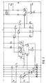
- FIG. 2 contains the complete circuit diagram for an exemplary embodiment of the EXOR gate according to the invention.
- the components of the EXOR gate according to FIG. 1 can be seen, all designations being retained, even for the parts of FIG. 1 which remain the same.
- the upper input stage for the first input signal u E1 is provided behind the input transistors EF1 and EF2 with subsequent emitter followers EF5 and EF6, which are coupled via diodes D1 and D2.
- the emitter resistors are the same for the input transistors with R2 or for the emitter followers with R3.
- This design means that the input stages are symmetrical and therefore offer the same input impedances.
- a second gate of the same design is provided for the actual EXOR gate, the two outputs being connected in parallel.
- this second current switch group is carried out in the same way as that of the first group, by now additionally controlling the lower pair of current switches T25 and T26 of the second EXOR gate from the two outputs of the additionally provided emitter followers of the upper input stage EF5 or EF6.
- the load resistors R1 are the same for both logic levels, and the supplying current sources are each designed for half the current i0 / 2.
- the structure and function of the output buffer corresponds to the output buffer of the EXOR gate according to FIG. 1.
Abstract
Description
Die Erfindung betrifft eine Schaltungsanordnung zur ausschließenden Oder-Verknüpfung zweier Signale gemäß Oberbegriff des Patentanspruches 1.The invention relates to a circuit arrangement for the exclusive OR combination of two signals according to the preamble of claim 1.
Durch die US-A-4,408,134 ist ein EXOR-Gatter in ECL-Technik bekannt geworden, bei dem die beiden Eingänge A und B mit den Basisanschlüssen von jeweils einem Stromschaltertransistor von übereinander angeordneten Stromschalterpaaren verbunden sind (21, 24 u. 25; Figur 2). Die Basen der jeweils anderen Stromschaltertransistoren (22, 23 u. 26) sind mit den internen Referenzspannungsquellen (VBB₁) bzw. VBB₂) verbunden. Die Kollektorströme der Transistoren 21 u. 23 fließen durch den gemeinsamen Lastwiderstand 28, an dem ein Spannungssignal abfällt, welches die ausschließende Oder-Verknüpfung der an den Eingängen A u. B anliegenden Signale darstellt. Dieses Ausgangssignal gelangt über den Emitterfolger 27 an den Ausgangsknoten 17 des EXOR-Gatters.An EXOR gate in ECL technology has become known from US Pat. No. 4,408,134, in which the two inputs A and B are connected to the base connections of a respective current switch transistor of pairs of current switches arranged one above the other (21, 24 and 25; FIG. 2 ). The bases of the other current switch transistors (22, 23 and 26) are connected to the internal reference voltage sources (V BB ₁) and V BB ₂). The collector currents of the transistors 21 u. 23 flow through the common load resistor 28, at which a voltage signal drops, which is the exclusive OR combination of the inputs A u. B represents signals present. This output signal arrives at the
Durch den Aufsatz "Grundschaltungen für digitale, bipolare Hochgeschwindigkeits-ICs" von I. Martiny in Elektronik Band 36, Nr. 19, 18. Sept. 1987, Seiten 140-146, ist ein EXOR-Gatter in DECL-Technik beschrieben, dessen Grundstruktur aus der analogen Signalverarbeitung bekannt ist und wobei Inverter mit Stromquellen- und Referenzspannungsgegenkopplungen, mit Eingangspaaren, an denen jeweils 2 zueinander logisch komplementäre Signale anstehen, und mit Emitterfolgern zur Potentialverschiebung verwendet werden.The article "Basic Circuits for Digital, Bipolar High-Speed ICs" by I. Martiny in Electronics Volume 36, No. 19, Sept. 18, 1987, pages 140-146 describes an EXOR gate in DECL technology, the basic structure of which is described is known from analog signal processing and inverters with current source and reference voltage negative feedback, with input pairs, each of which has 2 signals that are logically complementary to one another queue, and used with emitter followers for potential shift.
Eine verbesserte Schaltungsanordnung zur ausschließenden Oder-Verknüpfung zweier Signale ist in Figur 1 dargestellt. Diese Anordnung ist in Emitter-Emitter-Coupled-Logic (E²CL-) Technik ausgeführt. Aber auch diese verbesserte Anordnung weist noch einige Nachteile auf. Um diese Nachteile im folgenden verdeutlichen zu können, wird kurz auf die Aufgabe der einzelnen Funktionsblöcke eingegangen.An improved circuit arrangement for the exclusive OR combination of two signals is shown in FIG. 1. This arrangement is implemented using emitter-emitter-coupled logic (E²CL) technology. But this improved arrangement also has some disadvantages. In order to clarify these disadvantages in the following, it is brief discussed the task of the individual function blocks.
Eine erste Eingangsstufe für das Eingangssignal UE1 besteht aus den Eingangstransistoren EF₁ und EF₂ in Emitter-Schaltung. Eine zweite Eingangsstufe für das Eingangssignal UE2 besteht aus den beiden Eingangstransistoren EF₃ und EF₄ jeweils in Emitter-Schaltung, denen jeweils mittels einer Diode D₁ bzw. D₂ ein Emitterfolger EF₇ bzw. EF₈ nachgeschaltet sind. Die Eingangsstufen dienen sowohl der Pegelanpassung auch der Entkopplung des eigentlichen EXOR-Gatters von der ansteuernden Schaltung. Die Transistoren der Eingangsstufen sind jeweils mit ihren Kollektoren an Masse und über ihre Emitterwiderstände R₂, R₃ und R₄ an den Minuspol einer Betriebsspannungsquelle UB angeschaltet. Das eigentliche EXOR-Gatter besteht aus Stromschaltern, die übereinander angeordnet sind (Series Gating). Durch diese serielle Hintereinanderschaltung ist eine Pegelverschiebung zwischen den beiden Eingangssignalen des eingentlichen EXOR-Gatters notwendig. Dies wird durch das Diodenpaar D₁, D₂ und das Emitterfolgerpaar EF₇ bzw. EF₈ erreicht. Die Potentialdifferenz zwischen den beiden internen Signalebenen beträgt somit im Beispiel 2 x Basisemitterspannung.
Zur Logischen Verknüpfungen der beiden Eingangssignale dienen die genannten Stromschalter mit den Transistoren T₁ bis T₆. Das untere Stromschalterpaar mit den Transistoren T₅ und T₆ ist emittergekoppelt und über eine Stromquelle I₀ mit dem Minuspol der Betriebsspannungsquelle UB verbunden. Seine Basiseingänge werden von den Ausgängen der Emitterfolger EF₇ bzw. EF₈ angesteuert. An den beiden Kollektorausgängen i₅ und i₆ sind nun jeweils ein oberes Paar von weiteren Stromschaltern angeschaltet. Das erste Paar dieser jeweils ebenfalls emittergekoppelten Transistorpaare besteht aus den Transistoren T₁, T₂ bzw. T₃ und T₄. Die beiden Basiseingänge des ersten Paares T₁, T₂ werden von den Emitterausgängen der ersten Eingangsstufe EF₁ bzw. EF₂ angesteuert, während die Basiseingänge des zweiten Paares T₃ und T₄ invers dazu von den Emitterausgängen derselben genannten Eingangsstufe angesteuert werden. Die vier Kollektorausgänge der beiden oberen Stromschalterpaare sind paarweise parallelgeschaltet, i₁ mit i₃ und i₂ mit i₄, und jeweils über Lastwiderstände R₁ mit Massepotential (Pluspotential) der Betriebsspannungsquelle UB verbunden. Das Differenzausgangssignal ist an diesen Lastwiderständen R₁ abnehmbar. Zur Regeneration der Signalpegel sowie zur Entkopplung des eigentlichen EXOR-Gatters vom Ausgang dient eine nachgeschaltete Bufferstufe, die im Beispiel aus zwei Emitterfolgerpaaren EF₉, EF₁₁; EF₁₀, EF₁₂ mit den Emitterwiderständen R₅, R₆; R₅, R₆ mit dem Minuspol der Betriebsspannungsquelle verbunden sind, und einem Stromschalter mit den ebenfalls emittergekoppelten Transistoren T₈, T₉, deren gemeinsamer Emitter über eine Steuerspannung Uref steuerbare Stromquelle aus der Reihenschaltung eines Transistors T₁₀ und ein Widerstand R₇ mit dem Minuspol der Betriebsspannungsquelle verbunden ist, und dessen beiden Kollektorausgänge mit externen Lastwiderständen 2 x R₈ mit Massepotential verbunden sind, besteht.A first input stage for the input signal U E1 consists of the input transistors EF₁ and EF₂ in an emitter circuit. A second input stage for the input signal U E2 consists of the two input transistors EF₃ and EF₄ each in an emitter circuit, each of which is followed by an emitter follower EF₇ or EF₈ by means of a diode D₁ or D₂. The input stages serve both for level adjustment and for decoupling the actual EXOR gate from the driving circuit. The transistors of the input stages are each connected to ground by their collectors and via their emitter resistors R₂, R₃ and R₄ to the negative pole of an operating voltage source U B. The actual EXOR gate consists of current switches that are arranged one above the other (series gating). This serial connection in series means that a level shift between the two input signals of the ordinary EXOR gate is necessary. This is through the diode pair D₁, D₂ and the emitter follower pair EF₇ or EF₇ reached. The potential difference between the two internal signal levels is thus 2 x base emitter voltage in the example.
The current switches mentioned with the transistors T₁ to T₆ are used for logic operations of the two input signals. The lower pair of current switches with the transistors T₅ and T₆ is emitter-coupled and connected via a current source I₀ to the negative pole of the operating voltage source U B. Its basic inputs are controlled by the outputs of the emitter followers EF₇ and EF₈. An upper pair of further current switches are now connected to the two collector outputs i₅ and i₆. The first pair of these each also emitter-coupled transistor pairs consists of the transistors T₁, T₂ or T₃ and T₄. The two base inputs of the first pair T₁, T₂ are driven by the emitter outputs of the first input stage EF₁ or EF₂, while the base inputs of the second pair T₃ and T₄ are inversely controlled by the emitter outputs of the same input stage. The four collector outputs of the two upper pairs of current switches are connected in parallel in pairs, i₁ with i₃ and i₂ with i₄, and each connected via load resistors R₁ to ground potential (plus potential) of the operating voltage source U B. The differential output signal is removable at these load resistors R 1. A downstream buffer stage is used to regenerate the signal levels and to decouple the actual EXOR gate from the output, which in the example consists of two pairs of emitter followers EF₉, EF₁₁; EF₁₀, EF₁₂ with the emitter resistors R₅, R₆; R₅, R₆ are connected to the negative pole of the operating voltage source, and a current switch with the likewise emitter-coupled transistors T₈, T₉, whose common emitter can be controlled from the current source via a control voltage U ref Series connection of a transistor T₁₀ and a resistor R₇ is connected to the negative pole of the operating voltage source, and its two collector outputs are connected to external load resistors 2 x R₈ to ground potential.
Wechselt an einem Eingang des EXOR-Gatters der Signalpegel, während der Pegel am anderen Eingang konstant bleibt, so ändert sich die Spannung am Ausgang des EXOR-Gatters. Werden beide Eingangspegel gleichzeitig umgeschaltet, so wird bei einer idealen EXOR-Verknüpfung das Ausgangssignal nicht beeinflußt. Weil jedoch während des Umschaltens die Differenzspannung an den Stromschaltereingängen beider Signalebenen kurzzeitig den Wert 0 Volt annimmt, fließt der Strom I₀ in diesem Moment zu gleichen Teilen durch die beiden Lastwiderstände R₁. Hierdurch vermindert sich der Betrag der EXOR-Ausgangsspannung, bevor sich wieder der ursprüngliche positive oder negative Maximalwert der Ausgangsspannung einstellt. Im ungünstigsten Fall bricht die Differenzausgangsspannung auf 0 Volt zusammen.If the signal level changes at one input of the EXOR gate while the level at the other input remains constant, the voltage at the output of the EXOR gate changes. If both input levels are switched over at the same time, the output signal is not affected by an ideal EXOR operation. However, because during the switchover the differential voltage at the power switch inputs of both signal levels temporarily takes the value 0 volts, the current I Strom flows in equal parts through the two load resistors R₁ at this moment. This reduces the amount of the EXOR output voltage before the original positive or negative maximum value of the output voltage is restored. In the worst case, the differential output voltage collapses to 0 volts.
Die Nachteile des EXOR-Gatters zeigen sich bei folgenden verschiedenen Anwendungen.
- 1. Frequenzabhängige Laufzeitdifferenz zwischen den Signalebenen.
Die logische Verknüpfung der Eingangssignalen findet in den Transistoren T₁ bis T₄ statt. Der Signalfluß dorthin erfolgt auf 2 unterschiedlichen Wegen. Während das eine Eingangssignal über den Emitterfolger EF₁ an die Basen von T₁ und T₄ bzw. über EF₂ an die Basen von T₂ und T₃ gelangt, fließt das andere Eingangssignal über EF₃/D₁/EF₇ und T₅ zu den Emittern von T₁/T₂ bzw. über EF₄/D₂/EF₈ und T₆ zu den Emittern von T₃/T₄. Aufgrund der endlichen Schaltgeschwindigkeit der Transistoren wird die Laufzeit in den verschiedenen Signalwegen unterschiedlich.
Dadurch entsteht zwischen den zu verknüpfenden Signalen eine Laufzeitdifferenz tL, die sich bei den unterschiedlichen Anwendungsmöglichkeiten des EXOR-Gatters wie folgt auswirkt:- 1.1 Zur Frequenzverdoppelung werden an die beiden Eingänge des EXOR-Gatters periodische Signale gelegt, die lediglich eine geeignete Phasendifferenz aufweisen, z. B.:


Das EXOR-Gatter verhält sich bei der Frequenzverdoppelung dann ideal, wenn gilt
- 1.2 Differenzieren und Gleichrichten.
Beim Differenzieren und Gleichrichten wird eine beliebige Bitfolge direkt auf den einen EXOR-Eingang und die gleiche Bitfolge verzögert auf den anderen EXOR-Eingang gelegt. Der Ausgangsignalpegel ändert sich dadurch bei jeder Flanke des Eingangssignals, wodurch eine Taktrückgewinnung aus der Bitfolge möglich ist. Bei dieser Anwendung weist das beschriebene EXOR-Gatter folgende Nachteile auf. Die ansteigende und die abfallende Flanke des Ausgangssignals haben unterschiedliche Flankensteilheiten, da die Signalwege zu oberen und zur unteren Stromschalterebene unterschiedliches Tiefpaßverhalten aufweisen. Die Kurvenform des Ausgangssignals kann also unsymmetrisch werden und hängt davon ab, welche Signalebene direkt und welche verzögert angesteuert wird. - 1.3 Anwendung als Phasendetektor
Steuert man das EXOR-Gatter wie unter 1.1 an, so ist die Ausgangsgleichspannung ein Maß für die Phasenverschiebung zwischen den beiden Eingangstaktsignalen:
- 1.4 Logische Verknüpfung von Bitfolgen.
Legt man an die beiden EXOR-Eingänge beliebige Bitfolgen, so darf die EXOR-Ausgangsspannung ihren Pegel jeweils dann ändern, wenn sich nur eine der beiden Eingangsspannungen ändert. Die bereits im Abschnitt 1 definierte Laufzeitdifferenz ΔtL zwischen den verschiedenen Signalwegen führt zu einem entsprechenden Jitter des Ausgangssignals, der wegen der Frequenzabhängigkeit nicht breitbandig kompensierbar ist.
Wie in Abschnitt 1.2 besprochen, kann darüberhinaus die Flankensteilheit des Ausgangssignals davon abhängig sein, in welcher Stromschalteebene die Umschaltung erfolgt.
- 1.1 Zur Frequenzverdoppelung werden an die beiden Eingänge des EXOR-Gatters periodische Signale gelegt, die lediglich eine geeignete Phasendifferenz aufweisen, z. B.:
- 2. Eingangsimpedanz
Aufgrund der Schaltungsunsymmetrie haben die beiden EXOR-Eingänge unterschiedliche Eingangs-Impedanzen. Dadurch bedingt werden die Eingangs-Signalquellen unterschiedlich stark belastet. Außerdem unterscheiden sich die Reflektionsfaktoren der beiden Eingänge.
- 1. Frequency-dependent difference in transit time between the signal levels.
The logical combination of the input signals takes place in the transistors T₁ to T₄. The signal flow there is done in two different ways. While one input signal via the emitter follower EF₁ arrives at the bases of T₁ and T₄ or via EF₂ at the bases of T₂ and T₃, the other input signal flows via EF₃ / D₁ / EF₇ and T₅ to the emitters of T₁ / T₂ or respectively EF₄ / D₂ / EF₈ and T₆ to the emitters of T₃ / T₄. Due to the finite switching speed of the transistors, the transit time is different in the different signal paths.
This creates a transit time difference t L between the signals to be linked, which has the following effects for the different possible uses of the EXOR gate:- 1.1 For frequency doubling periodic signals are applied to the two inputs of the EXOR gate, which only have a suitable phase difference, z. B .:
When doubling the frequency, the EXOR gate behaves ideally when it applies - 1.2 Differentiate and rectify.
When differentiating and rectifying, any bit sequence is directly delayed to one EXOR input and the same bit sequence delayed to the other EXOR input laid. As a result, the output signal level changes on every edge of the input signal, which enables clock recovery from the bit sequence. In this application, the EXOR gate described has the following disadvantages. The rising and falling edges of the output signal have different steepnesses, since the signal paths to the upper and lower current switch levels have different low-pass behavior. The waveform of the output signal can therefore become asymmetrical and depends on which signal level is controlled directly and which is delayed. - 1.3 Use as a phase detector
If you control the EXOR gate as in 1.1, the DC output voltage is a measure of the phase shift between the two input clock signals: - 1.4 Logical combination of bit sequences.
If any bit sequences are applied to the two EXOR inputs, the EXOR output voltage may change its level if only one of the two input voltages changes. The transit time difference .DELTA.t L already defined in section 1 between the different signal paths leads to a corresponding jitter of the output signal, which cannot be compensated for over a wide band because of the frequency dependence.
As discussed in section 1.2, the slope of the output signal can also depend on the current switching level at which the switchover takes place.
- 1.1 For frequency doubling periodic signals are applied to the two inputs of the EXOR gate, which only have a suitable phase difference, z. B .:
- 2. Input impedance
Due to the circuit asymmetry, the two EXOR inputs have different input impedances. As a result, the input signal sources are loaded to different extents. In addition, the reflection factors of the two inputs differ.
Der Erfindung lag deshalb die Aufgabe zugrunde, eine Schaltungsanordnung der eingangs genannten Art anzugeben, die in der Lage ist die geschilderten Nachteile zu eliminieren. Der Aufwand hierzu soll nicht allzu hoch sein.The invention was therefore based on the object of specifying a circuit arrangement of the type mentioned at the outset which is capable of eliminating the disadvantages described. The effort for this should not be too high.
Die Lösung dieser Aufgabe erfolgt durch die Merkmale des Patentanspruches 1.This object is achieved by the features of patent claim 1.
Das erfindungsgemäße ausschließende Oder-Gatter weist die Vorteile auf, daß beide Eingangsstufen dieselben Eingangsimpedanzen haben, daß gleiche Schalt- und Signallaufzeiten auftreten.
Der Erfindung lag die grundlegende Idee zugrunde, das eingangs genannte EXOR-Gatter vollkommen symmetrisch aufzubauen. Im einzelnen werden dabei die Eingangsstufen des erfindungsgemäßen EXOR-Gatters so ausgelegt, daß beide Eingangssignale sowohl auf eine obere als auch mit verschobenen Pegeln auf eine untere Stromschalterebene gelegt werden; dadurch wird gewährleistet, daß beide Eingänge dieselbe Eingangsimpedanz aufweisen. Zum anderen wird die obere Stufe des EXOR-Gatters, in der die logische Verknüpfung erfolgt, zweifach ausgeführt. Durch die doppelte Ausführung der Verknüpfungsstufen wird es ermöglicht, daß bei jedem Pegelwechsel an einem EXOR-Eingang immer sowohl eine obere als auch eine untere Stromschalterebene umgeschaltet wird. Dadurch werden gleiche Schalt- und Signallaufzeiten erreicht, unabhängig davon, an welchem Eingang ein Pegelwechsel erfolgt.The exclusive OR gate according to the invention has the advantages that both input stages have the same input impedances, that the same switching and signal propagation times occur.
The invention was based on the basic idea of constructing the EXOR gate mentioned at the outset in a completely symmetrical manner. Specifically, the input stages of the EXOR gate according to the invention are designed so that both input signals are placed on an upper as well as with shifted levels on a lower current switch level; this ensures that both inputs have the same input impedance. On the other hand, the upper stage of the EXOR gate, in which the logic operation takes place, is carried out twice. The double execution of the linkage levels will enables an upper and lower current switch level to be switched at every level change at an EXOR input. This means that the same switching and signal propagation times are achieved, regardless of the input at which a level change takes place.
Die abhängigen Ansprüche stellen vorteilhafte Ausgestaltungen der Erfindung dar.The dependent claims represent advantageous embodiments of the invention.
Es erfolgt nun die Beschreibung anhand der Figur 2, welche das vollständige Schaltbild für ein Ausführungsbeispiel des erfindungsgemäßen EXOR-Gatters beinhaltet.
Erkennbar sind die Bestandteile des EXOR-Gatters gemäß Figur 1, wobei alle Bezeichnungen, auch für die darüberhinaus gleichgebliebenden Teile der Figur 1, beibehalten sind.The description will now be made with reference to FIG. 2, which contains the complete circuit diagram for an exemplary embodiment of the EXOR gate according to the invention.
The components of the EXOR gate according to FIG. 1 can be seen, all designations being retained, even for the parts of FIG. 1 which remain the same.
Erfindungsgemäß ist auch die obere Eingangsstufe für das erste Eingangssignal uE1 hinter den Eingangstransistoren EF₁ und EF₂ mit nachfolgenden Emitterfolgern EF₅ und EF₆ versehen, welche über Dioden D₁ und D₂ angekoppelt sind. Die Emitterwiderstände sind für die Eingangstransistoren mit R₂ bzw. für die Emitterfolger mit R₃ jeweils gleich. Durch diesen Aufbau sind die Eingangsstufen symmetrisch und bieten damit gleiche Eingangsimpedanzen. Zu dem eigentlichen EXOR-Gatter ist ein zweites gleichartig aufgebautes Gatter vorgesehen, wobei die beiden Ausgänge parallel geschaltet sind. Die Ansteuerung dieser zweiten Stromschaltergruppe erfolgt in der gleichen Weise wie die der ersten Gruppe, indem nunmehr zusätzlich das untere Stromschalterpaar T₂₅ und T₂₆ des zweiten EXOR-Gatters von den beiden Ausgängen der zusätzlich vorgesehenen Emitterfolger der oberen Eingangsstufe EF₅ bzw. EF₆ angesteuert werden. In entsprechender Weise werden die Basiseingänge der beiden oberen Stromschalterpaare T₂₁, T₂₂ bzw. T₂₃, T₂₄ des zweiten EXOR-Gatters von den Emitter-Ausgängen der Eingangstransistoren EF₃ bzw. EF₄ der unteren Eingangsstufe angesteuert.
Gemäß dem Realisierungsbeispiel nach Figur 2 sind die Lastwiderstände R₁ für beide Verknüpfungsstufen dieselben, und die speisenden Stromquellen sind in entsprechender Weise jeweils für den halber Strom i₀/2 ausgelegt.
Der Ausgangsbuffer entspricht in Aufbau und Funktion dem Ausgangsbuffer des EXOR-Gatters nach Figur 1.According to the invention, the upper input stage for the first input signal u E1 is provided behind the input transistors EF₁ and EF₂ with subsequent emitter followers EF₅ and EF₆, which are coupled via diodes D₁ and D₂. The emitter resistors are the same for the input transistors with R₂ or for the emitter followers with R₃. This design means that the input stages are symmetrical and therefore offer the same input impedances. A second gate of the same design is provided for the actual EXOR gate, the two outputs being connected in parallel. The control of this second current switch group is carried out in the same way as that of the first group, by now additionally controlling the lower pair of current switches T₂₅ and T₂₆ of the second EXOR gate from the two outputs of the additionally provided emitter followers of the upper input stage EF₅ or EF₆. In a corresponding manner, the base inputs of the two upper pairs of current switches T₂₁, T₂₂ and T₂₃, T₂₄ of the second EXOR gate of the Emitter outputs of the input transistors EF₃ or EF₄ the lower input stage driven.
According to the implementation example of Figure 2, the load resistors R₁ are the same for both logic levels, and the supplying current sources are each designed for half the current i₀ / 2.
The structure and function of the output buffer corresponds to the output buffer of the EXOR gate according to FIG. 1.
Die Vorteile des erfindungsgemäßen EXOR-Gatters im Einzelnen:
- 1. Einsatz des EXOR-Gatters als Frequenzverdoppler.
Beim Einsatz des EXOR-Gatters als Frequenzverdoppler (Eingangsspannungen uE1 und uE2 laut Definition in Abschnitt 1.1) erhält man eine Ausgangsspannung, die im Idealfall gleichspannungsfrei ist und deren Tastverhältnis 1:1 ist.
Berücksichtigt man den durch die unterschiedlichen Signalwege zu den oberen und unteren Stromschalterebenen hervorgerufenen Laufzeitunterschied zwischen den Eingangssignalen durch einen zusätzlichen Phasenwinkel , so läßt sich beim Einsatz des Doppel-EXOR-Gatter als Frequenzverdoppler für die Ausgangsgleichspannung uA=, folgender Zusammenhang herleiten (vgl. Diplomarbeit L. Schmidt):
- 2. Differenzieren und Gleichrichten
Bei Verwendung des EXOR-Gatters zum Differenzieren und Gleichrichten einer beliebigen Bitfolge entfallen die oben beschriebenen Nachteile des EXOR-Gatters.
Die ansteigende und die abfallende Flanke besitzen hier die gleiche Flankensteilheit, weil bei jedem Schaltvorgang sowohl eine untere als auch eine obere Stromschalterebene umgeschaltet werden, d. h. die RC-Zeitkonstanten sowie die Transistorschaltzeiten beider Signalwege beeinflussen in gleicher Weise beide Flanken des Ausgangssignals.
Hieraus folgt auch, daß das Ausgangssignal gleiche Flankensteilheiten besitzt und daß die Kurvenform des Ausgangssignals unabhängig davon ist, welcher der beiden Doppel-EXOR-Eingänge direkt und welcher verzögert angesteuert wird. - 3. Anwendung des EXOR-Gatters als Phasendetektor Steuert man das EXOR-Gatter so mit einem periodischen Signal an, daß zwischen den sonst gleichen EXOR-Eingangsspannungen lediglich eine Phasenverschiebung besteht, so ergibt sich für den Gleichspannungsanteil uA= des Ausgangssignals der in Gleichung (2) angegebenen Wert. Die maximale Empfindlichkeit duA=/dφ, die bei ∇ = π/2 auftritt, ist zwar um den Faktor cos |ζ(ω)| geringer als beim Standard-EXOR-Gatter jedoch im Gegensatz zu diesem frequenzunabhängig. Somit ist auch der Symmetriepunkt der Funktion uA= =f (φ) frequenzunabhängig.
- 4. Logische Verknüpfung von Bitfolgen
Da beim EXOR-Gatter immer sowohl eine obere als auch eine untere Stromschalterebene umschaltet, unabhängig davon welcher der beiden Eingangs-Spannungspegel wechselt, ist die Signallaufzeit zwischen dem Empfang und dem Ausgang konstant.
Die frequenzabhängige Laufzeitdifferenz zwischen den Signalen an den oberen und den unteren Stromschalterebenen der Verknüpfungsstufen führt hier also nicht zu einem Jitter des Ausgangssignals.
Die Flankensteilheit des Ausgangssignals ist beim völlig symmetrischen EXOR-Eingang immer gleich, unabhängig davon, an welchem EXOR-Eingang ein Pegelwechsel erfolgt. Sie ist allerdings etwas geringer als beim Standard-EXOR.
Das erfindungsgemäße Gatter erweist sich also bei allen o.g. typischen EXOR-Anwendungen als vorteilhaft gegenüber dem EXOR-Gatter nach Figur 1.
Der Mehraufwand an Schaltelementen stellt bei der monolithischen Integration demgegenüber keinen wesentlichen Nachteil der.
Die im vorigen Abschnitt 4. erwähnte etwas geringere Flankensteilheit kann am Ausgang der Verknüpfungsstufe durch eine zusätzliche Versteilerungsstufe ausgeglichen werden. - 5. Anwendung des EXOR-Gatters als Multiplizierer Das erfindungsgemäße EXOR-Gatter läßt sich mit geringen Änderungen vorteilhaft auch als analoger Multiplizierer verwenden. Diese Änderungen sind in Figur 3 dargestellt, welche im Prinzip die
Schaltungsanordnung nach Figur 2 zeigt, ergänzt um einige weitere Bauteile.
Wenn zwei Ergänzungen des Schaltungskonzepts nach Figur 2 vorgenommen werden, liegt mit der Schaltung ein analoger Multiplizierer mit großem Dynamikbereich der Eingangsspannungen vor. Diese beiden Ergänzungen sind folgende:
Zum einen wird die Schaltungsanordnung zur Erhöhung des Linearitätsbereichs der Stromschalter in der oberen Ebene, das sind die Transistoren T₁₁ bis T₁₄ sowie T₂₁ bis T₂₄ um zwei Vorverzerrerstufen erweitert.
Zum andern werden in die beiden Stromschalter der unteren Stromschalterebene der Stromschaltergruppen, das sind die Transistoren T₁₅, T₁₆ und T₂₅, T₂₆,Gegenkopplungswiderstände R₆ zur Erhöhung des Linearitätsbereichs eingefügt. Diese Maßnahme wird auch bei den Vorverzerrern eingeführt, nämlich mit den Gegenkopplungswiderständen R₅ bei den Transistoren T₁₇, T₁₈ der ersten Vorverzerrerstufe und den Transistoren T₂₇, T₂₈ der zweiten Vorverzerrerstufe. Die Emitter der beiden Stromschalterpaare der Vorverzerrerstufen sind jeweils über diese Gegenkopplungswiderstände R₅ mit den Stromquellen, bestehend aus TS₁ und deren Emitterwiderstände R₈ verbunden. Die Kollektoren der genannten Stromschaltertransistoren sind über die Diodenpaare D₁₁, D₁₂ bzw. D₂₁, D₂₂ und die Pegelverschiebungswiderstände R₇ mit dem Pluspol, Masse, der Betriebsspannungsquelle verbunden. An den Verbindungspunkten zwischen den Dioden und ihren Kollektoren werden die zur Ansteuerung der oberen Stromschalterebene benötigten Signale abgegriffen, wobei also die Basen der Transistorpaare der oberen Stromschalterebene jeweils kreuzweise miteinander und mit dem zugehörigen Kollektor der entsprechenden Vorverzerrerstufe verbunden sind. Die ansteuernden Signale für die Vorverzerrerstufen werden ebenso wie die ansteuernden Signale der unteren Stromschalterebene hinter den Emitterfolgerpaaren EF₅ und EF₆ bzw. EF₇, EF₈ abgenommen. Die Abgriffe hinter den Emitterfolgerpaaren EF₁, EF₂ sowie EF₃, EF₄, die beim Doppel-EXOR-Gatter gemäß Figur 2 zur Ansteuerung der oberen Stromschalter erforderlich sind, entfallen hier.
Die Vorteile des Doppel-EXOR-Gatters gelten im selben Maße auch für den Multiplizierer.
Die gegenüber bekannten Multipliziererkonzepten erhöhte Zahl der benötigten Transistoren stellt bei der monolithischen Integration keinen wesentlichen Nachteil dar.
- 1. Use of the EXOR gate as a frequency doubler.
When the EXOR gate is used as a frequency doubler (input voltages u E1 and u E2 as defined in section 1.1), an output voltage is obtained which is ideally DC-free and whose duty cycle is 1: 1.
If one takes into account the delay time difference between the input signals caused by the different signal paths to the upper and lower current switch levels, an additional phase angle can be used to derive the following relationship when using the double EXOR gate as a frequency doubler for the DC output voltage u A = (see diploma thesis L. Schmidt): - 2. Differentiate and rectify
When using the EXOR gate to differentiate and rectify any bit sequence, the Disadvantages of the EXOR gate described above.
The rising and the falling edge have the same edge steepness here, because with each switching operation both a lower and an upper current switch level are switched, i.e. the RC time constants and the transistor switching times of both signal paths influence both edges of the output signal in the same way.
It also follows from this that the output signal has the same slope and that the curve shape of the output signal is independent of which of the two double EXOR inputs is controlled directly and which is triggered with a delay. - 3.Use of the EXOR gate as a phase detector If the EXOR gate is controlled with a periodic signal such that there is only a phase shift between the otherwise identical EXOR input voltages, the DC voltage component u A = of the output signal of the equation ( 2) specified value. The maximum sensitivity du A = / dφ that occurs at ∇ = π / 2 is by the factor cos | | (ω) | less than the standard EXOR gate, however, in contrast to this, independent of frequency. The point of symmetry of the function u A = = f (φ) is therefore frequency-independent.
- 4. Logical combination of bit sequences
Since the EXOR gate always switches both an upper and a lower current switch level, regardless of which of the two input voltage levels changes, the signal delay between reception and output is constant.
The frequency-dependent transit time difference between the signals at the upper and lower current switch levels of the logic stages does not lead to jitter in the output signal here.
The edge steepness of the output signal is always the same for the completely symmetrical EXOR input, regardless of the EXOR input at which a level change takes place. However, it is somewhat lower than that of the standard EXOR.
The gate according to the invention thus proves to be advantageous over the EXOR gate according to FIG.
In contrast, the additional expenditure on switching elements in the case of monolithic integration does not represent a significant disadvantage of.
The somewhat lower edge steepness mentioned in the previous section 4 can be compensated for at the output of the logic stage by an additional steepening stage. - 5. Use of the EXOR gate as a multiplier The EXOR gate according to the invention can advantageously also be used as an analog multiplier with minor changes. These changes are shown in FIG. 3, which in principle shows the circuit arrangement according to FIG. 2, supplemented by a few further components.
If two additions to the circuit concept according to FIG. 2 are made, the circuit is an analog multiplier with a large dynamic range of the input voltages. These two additions are as follows:
Firstly, the circuit arrangement for increasing the linearity range of the current switches in the upper level, that is, the transistors T₁₁ to T₁₄ and T₂₁ to T₂₄ expanded by two predistortion stages.
On the other hand, the two power switches on the lower power switch level of the power switch groups, that is Transistors T₁₅, T₁₆ and T₂₅, T₂₆, negative feedback resistors R₆ inserted to increase the linearity range. This measure is also introduced in the predistorters, namely with the negative feedback resistors R₅ for the transistors T₁₇, T₁₈ of the first predistortion stage and the transistors T₂₇, T₂₈ of the second predistortion stage. The emitters of the two pairs of current switches of the predistorter stages are each connected via these negative feedback resistors R₅ to the current sources consisting of TS₁ and their emitter resistors R₈. The collectors of the current switch transistors are connected via the diode pairs D₁₁, D₁₂ or D₂₁, D₂₂ and the level shift resistors R₇ to the positive pole, ground, of the operating voltage source. At the connection points between the diodes and their collectors, the signals required to control the upper current switch level are tapped, so that the bases of the transistor pairs of the upper current switch level are each connected crosswise to one another and to the associated collector of the corresponding predistortion stage. The driving signals for the predistortion stages, like the driving signals of the lower power switch level, are taken after the emitter follower pairs EF₅ and EF₆ or EF₇, EF₈. The taps behind the emitter follower pairs EF₁, EF₂ and EF₃, EF₄, which are required in the double EXOR gate according to Figure 2 to control the upper current switch, are omitted here.
The advantages of the double EXOR gate also apply to the multiplier.
The increased number of transistors required compared to known multiplier concepts does not represent a significant disadvantage in monolithic integration.
Claims (11)
- A circuit arrangement for the exclusive OR linkage of two signals, the arrangement including a group of serially arranged current switches fed by a current source which is connected with the one pole of the operating voltage source, the arrangement further including a transistor input stage fed by the operating voltage source for the first input signal (UE1) and for the second input signal (UE2), with each transistor input stage being provided with a first input and a second input between which the respective input signal (UE1; UE2) is present and with first emitter followers (EF₁, EF₂; EF₃, EF₄) at its two inputs for level matching and decoupling; wherein, in order to shift the level of the second input signal (UE2), the outputs of the first emitter followers (EF₃; EF₄) provided in the transistor input stage for the second input signal (UE2) are connected with second emitter followers (EF₇; EF₈) that are each coupled by way of a diode (D₃; D₄), with the outputs of the second emitter followers actuating the bases of two first, common-emitter, push-pull transistor current switches (T₁₅, T₁₆) that are fed by the current source and the outputs of the first emitter followers (EF₁; EF₂) provided in the transistor input stage for the first input signal (UE1) each actuate the bases of two second transistor current switches (T₁₁, T₁₂) and two third transistor current switches (T₁₃, T₁₄), each coupled in pairs to have common emitters, operating in push-pull and being serially connected in the collector path of the first transistor switches (T₁₅, T₁₆), with the collectors of the one second current switch (T₁₁) and the one third current switch (T₁₃) and the collectors of the other second current switch (T₁₂) and the other third current switch (T₁₄) being connected together; the one second current switch (T₁₁) and the other third current switch (T₁₄) are actuated, by way of the respective emitter follower, by the signal at the first input of the transistor input stage for the first input signal (UE1); and the other second current switch (T₁₂) and the one third current switch (T₁₃) are actuated, by way of the respective emitter follower, by the signal at the second input of the transistor input stage for the first input signal (UE1); and the two interconnected collector pairs of the second current switches (T₁₁, T₁₂) and of the third current switches (T₁₃, T₁₄) are connected, in each case by way of the same size load resistance (R₁), with the other pole of the operating voltage source, and the difference output signal (UA) of the circuit arrangement is obtained from the voltage difference between the two interconnected collector pairs,
characterized in that
the first emitter followers (EF₁; EF₂) provided in the transistor input stage for the first input signal (UE1) to shift the level of the first input signal (UE1) are each followed by second emitter followers (EF₅; EF₆) that are coupled together by way of a diode (D₁; D₂) and whose outputs actuate the bases of two fourth, common-emitter, push-pull transistor current switches (T₂₅, T₂₆) that are fed by the current source;
the outputs of the first emitter followers (EF₃; EF₄) provided in the transistor input stage for the second input signal (UE2) each actuate the bases of two fifth transistor current switches ((T₂₁, T₂₂) and two sixth transistor current switches (T₂₃, T₂₄), each coupled in pairs to have common emitters, operating in push-pull, and being serially connected in the collector path of the fourth transistor current switches (T₂₅, T₂₆) ;
the collectors of the one fifth current switch (T₂₁) and of the one sixth current switch (T₂₃) and the collectors of the other fifth current switch (T₂₂) and the other sixth current switch (T₂₄) are connected together, with the one fifth current switch (T₂₁) and the other sixth current switch (T₂₄) being actuated, by way of the respective emitter follower, by the signal at the first input of the transistor input stage for the second input signal (UE2), and the other fifth current switch (T₂₂) and the one sixth current switch (T₂₃) are actuated, by way of the respective emitter follower, by the signal at the second input of the transistor input stage for the second input signal (UE2); and
the two interconnected collector pairs of the fifth current switches (T₂₁, T₂₂) and the sixth current switches (T₂₃, T₂₄) are connected with the two interconnected collector pairs of the second current switch (T₁₁, T₁₂) and the third current switches (T₁₃, T₁₄) in such a manner that the collectors of the one second (T₁₁), third (T₁₃), fifth (T₂₁) and sixth (T₂₃) current switches and the collectors of the other second (T₁₂), third (T₁₄), fifth (T₂₂) and sixth (T₂₄) current switches are connected with one another. - A circuit arrangement according to Claim 1, characterized in that the first emitter follower stages (EF₁, EF₂; EF₃, EF₄) of the input stages each have the same emitter resistance (R₂).
- A circuit arrangement according to Claim 1 or 2, characterized in that the second emitter follower stages (EF₅, EF₆; EF₇, EF₈) of the input stages each have the same emitter resistance (R₃).
- A circuit arrangement according to Claim 1, 2 or 3, characterized in that the one group of the first, second and third current switches and the other group of the fourth, fifth and sixth current switches are each fed by a current source having the same current intensity (I₀/2).
- A circuit arrangement according to one of the preceding claims, characterized in that two predistortion stages (T₁₇, T₁₈; T₂₇, T₂₈) are provided which are each composed of two push-pull, common emitter transistors and are inserted between the outputs of the second emitter followers (EF₅, EF₆; EF₇, EF₈) of the transistor input stages for the first input signal (UE1) and the second input signal (UE2), respectively; and the inputs of the second and third and fifth and sixth current switches, respectively (T₁₁, T₁₂, T₁₃, T₁₄; T₂₁, T₂₂, T₂₃, T₂₄); and feedback resistances (R₅; R₆) are inserted on the emitter sides of the transistors of the two predistortion stages (T₁₇, T₁₈; T₂₇, T₂₈) and of the transistors (T₁₅, T₁₆; T₂₅, T₂₆) of the first and fourth current switches.
- A circuit arrangement according to Claim 5, characterized in that the bases of the emitter followers (EF₁, EF₂, EF₃, EF₄) of both transistor input stages are each connected via a resistor (R₄) with the one pole (ground) of the operating voltage.
- A circuit arrangement according to either Claim 5 or 6, characterized in that the bases of the transistor pairs (T₁₇, T₁₈; T₂₇, T₂₈) of the first and second predistortion stages, as well as the bases of the transistor pairs (T₂₅, T₂₆; T₁₅, T₁₆) of the fourth and first current switches are each connected with the emitters of the second emitter follower stage (EF₅, EF₆; EF₇, EF₈) of the first and second input stage, respectively.
- A circuit arrangement according to one of Claims 5 to 7, characterized in that the collectors of the transistor pairs of the predistortion stages are each connected, via decoupling diodes (D₁₁, D₁₂; D₂₁, D₂₂) and in series connected pairs via a common collector resistor (R₇; R₇), with the one pole (ground) of the operating voltage.
- A circuit arrangement according to one of Claims 5 to 8, characterized in that the two predistortion stages are each fed by a current source (TS₁, R₈).
- A circuit arrangement according to one of Claims 5 to 9, characterized in that, in the first predistortion stage, the collector of the one transistor (T₁₇) is connected with the bases of the one second current switch (T₁₁) and of the other third current switch (T₁₄) and the collector of the other transistor (T₁₈) is connected with the bases of the other second current switch (T₁₂) and the one third current switch (T₁₃); in the second predistortion stage, the collector of the one transistor (T₂₇) is connected with the bases of the one fifth current switch (T₂₁) and the other sixth current switch (T₂₄) and the collector of the other transistor (T₂₈) is connected with the bases of the other fifth current switch (T₂₂) and the one sixth current switch (T₂₃).
- A circuit arrangement according to one of the preceding claims, characterized by its configuration in E²CL technology.
Applications Claiming Priority (2)
| Application Number | Priority Date | Filing Date | Title |
|---|---|---|---|
| DE3829164 | 1988-08-27 | ||
| DE3829164A DE3829164C1 (en) | 1988-08-27 | 1988-08-27 |
Publications (2)
| Publication Number | Publication Date |
|---|---|
| EP0389577A1 EP0389577A1 (en) | 1990-10-03 |
| EP0389577B1 true EP0389577B1 (en) | 1993-09-15 |
Family
ID=6361755
Family Applications (1)
| Application Number | Title | Priority Date | Filing Date |
|---|---|---|---|
| EP89908152A Expired - Lifetime EP0389577B1 (en) | 1988-08-27 | 1989-07-15 | Circuits for exclusive disjunction of two signals |
Country Status (4)
| Country | Link |
|---|---|
| US (1) | US5122687A (en) |
| EP (1) | EP0389577B1 (en) |
| DE (1) | DE3829164C1 (en) |
| WO (1) | WO1990002451A1 (en) |
Families Citing this family (24)
| Publication number | Priority date | Publication date | Assignee | Title |
|---|---|---|---|---|
| DE3917714A1 (en) * | 1989-05-31 | 1990-12-06 | Siemens Ag | MULTIPLIZER CIRCUIT |
| WO1992011704A1 (en) * | 1990-12-21 | 1992-07-09 | Motorola, Inc. | Apparatus and method for generating quadrature signals |
| US5252865A (en) * | 1991-08-22 | 1993-10-12 | Triquint Semiconductor, Inc. | Integrating phase detector |
| US5489869A (en) * | 1994-05-17 | 1996-02-06 | Rockwell International | Antenna control unit attenuator and Bi-phase modulator |
| US5635863A (en) * | 1995-05-25 | 1997-06-03 | Vtc, Inc. | Programmable phase comparator |
| US5570056A (en) * | 1995-06-07 | 1996-10-29 | Pacific Communication Sciences, Inc. | Bipolar analog multipliers for low voltage applications |
| US5708383A (en) * | 1996-04-26 | 1998-01-13 | Nat Semiconductor Corp | Integrated circuit frequency controlled modulator for use in a phase lock loop |
| US6130602A (en) | 1996-05-13 | 2000-10-10 | Micron Technology, Inc. | Radio frequency data communications device |
| US6941124B1 (en) | 1996-05-13 | 2005-09-06 | Micron Technology, Inc. | Method of speeding power-up of an amplifier, and amplifier |
| US6774685B2 (en) | 1996-05-13 | 2004-08-10 | Micron Technology, Inc. | Radio frequency data communications device |
| US6836468B1 (en) | 1996-05-13 | 2004-12-28 | Micron Technology, Inc. | Radio frequency data communications device |
| US6696879B1 (en) * | 1996-05-13 | 2004-02-24 | Micron Technology, Inc. | Radio frequency data communications device |
| US6359486B1 (en) * | 2000-05-22 | 2002-03-19 | Lsi Logic Corporation | Modified phase interpolator and method to use same in high-speed, low power applications |
| DE10037478C1 (en) * | 2000-08-01 | 2001-08-09 | Siemens Ag | EXOR circuit |
| JP2005236600A (en) * | 2004-02-19 | 2005-09-02 | Matsushita Electric Ind Co Ltd | High frequency 2 multiplication circuit |
| US7298195B2 (en) * | 2005-03-31 | 2007-11-20 | Agere Systems Inc. | Methods and apparatus for improved phase switching and linearity in an analog phase interpolator |
| US20070124897A1 (en) * | 2005-12-01 | 2007-06-07 | Wilson Eric J | Clamp for circular objects |
| US20150009747A1 (en) * | 2013-07-02 | 2015-01-08 | Akbar Ghazinour | Phase switchable bistable memory device, a frequency divider and a radio frequency transceiver |
| US10594334B1 (en) | 2018-04-17 | 2020-03-17 | Ali Tasdighi Far | Mixed-mode multipliers for artificial intelligence |
| US10832014B1 (en) | 2018-04-17 | 2020-11-10 | Ali Tasdighi Far | Multi-quadrant analog current-mode multipliers for artificial intelligence |
| US10700695B1 (en) | 2018-04-17 | 2020-06-30 | Ali Tasdighi Far | Mixed-mode quarter square multipliers for machine learning |
| US11449689B1 (en) | 2019-06-04 | 2022-09-20 | Ali Tasdighi Far | Current-mode analog multipliers for artificial intelligence |
| US11416218B1 (en) | 2020-07-10 | 2022-08-16 | Ali Tasdighi Far | Digital approximate squarer for machine learning |
| US11467805B1 (en) | 2020-07-10 | 2022-10-11 | Ali Tasdighi Far | Digital approximate multipliers for machine learning and artificial intelligence applications |
Family Cites Families (9)
| Publication number | Priority date | Publication date | Assignee | Title |
|---|---|---|---|---|
| NL7007842A (en) * | 1969-06-09 | 1970-12-11 | ||
| US3838393A (en) * | 1973-12-17 | 1974-09-24 | Signetics Corp | Threshold logic gate |
| US4041326A (en) * | 1976-07-12 | 1977-08-09 | Fairchild Camera And Instrument Corporation | High speed complementary output exclusive OR/NOR circuit |
| US4408134A (en) * | 1981-01-19 | 1983-10-04 | Advanced Micro Devices, Inc. | Unitary exclusive or-and logic circuit |
| JPS58197920A (en) * | 1982-05-13 | 1983-11-17 | Toshiba Corp | Logical circuit |
| JPS60247733A (en) * | 1984-05-24 | 1985-12-07 | Toshiba Corp | Logical arithmetic circuit |
| JPS60247734A (en) * | 1984-05-24 | 1985-12-07 | Toshiba Corp | Logical arithmetic circuit |
| US4810908A (en) * | 1986-12-01 | 1989-03-07 | Hirokazu Suzuki | Semiconductor logic circuit comprising clock driver and clocked logic circuit |
| US4900954A (en) * | 1988-11-30 | 1990-02-13 | Siemens Components,Inc. | Mixed CML/ECL macro circuitry |
-
1988
- 1988-08-27 DE DE3829164A patent/DE3829164C1/de not_active Expired
-
1989
- 1989-07-15 WO PCT/DE1989/000470 patent/WO1990002451A1/en active IP Right Grant
- 1989-07-15 EP EP89908152A patent/EP0389577B1/en not_active Expired - Lifetime
- 1989-07-15 US US07/585,105 patent/US5122687A/en not_active Expired - Fee Related
Also Published As
| Publication number | Publication date |
|---|---|
| WO1990002451A1 (en) | 1990-03-08 |
| EP0389577A1 (en) | 1990-10-03 |
| US5122687A (en) | 1992-06-16 |
| DE3829164C1 (en) | 1989-08-10 |
Similar Documents
| Publication | Publication Date | Title |
|---|---|---|
| EP0389577B1 (en) | Circuits for exclusive disjunction of two signals | |
| DE4206082C1 (en) | ||
| DE19624270C2 (en) | Complementary clock generator for generating complementary clocks | |
| DE102005025443B4 (en) | Short circuit detection circuit and abnormality monitoring signal generation circuit | |
| DE3924593A1 (en) | DELAY DEVICE | |
| DE2611863A1 (en) | LEVEL CONVERTER FOR BINARY SIGNALS | |
| EP0208328A1 (en) | Dynamic control system | |
| DE2706904A1 (en) | BISTABLE CIRCUIT | |
| EP0957582B1 (en) | Circuit for generating complementary signals | |
| DE10130123A1 (en) | Delay control loop for generating complementary clock signals | |
| EP0025502A1 (en) | Bistable circuit with current distributing switches | |
| DE3924502C1 (en) | XOR coupling circuitry for two signals - has two pre=emphasis stages between input stages and two current-switching groups | |
| DE102006018236A1 (en) | Controllable power source for use in integrated circuit, comprises two supply terminals to build two supply potentials, where power source has replication of current paths in their uncontrolled condition | |
| EP1033814B1 (en) | Integrated circuit for generating two non-overlapping clock signals | |
| CH499928A (en) | Circuit arrangement for the electronic control of the feed current of an electrical load with predominantly inductive resistance | |
| DE3301866A1 (en) | ELECTRONIC CONTROL CIRCUIT FOR GENERATING A MONOSTABLE SWITCHING BEHAVIOR IN A BISTABLE RELAY | |
| EP0309769B1 (en) | Voltage-controlled oscillator comprising a ceramic crystal | |
| DE4015032A1 (en) | AMPLIFIER WITH REINFORCEMENT ONE WITH HIGH RISE AND DECLINE SPEED AND LARGE WIDTH | |
| EP0623998A1 (en) | Circuit to generate two complementary signals | |
| EP0029480A1 (en) | Emitter follower logic circuit | |
| DE4324854C1 (en) | Output stage for digital power switches | |
| DE2039732A1 (en) | Circuit arrangement for the derivation of pulses | |
| DE2139312C3 (en) | Temperature compensated ECL circuit | |
| DE1512416C (en) | Link | |
| EP0614277A1 (en) | Delay line circuit in a CMOS integrated circuit |
Legal Events
| Date | Code | Title | Description |
|---|---|---|---|
| PUAI | Public reference made under article 153(3) epc to a published international application that has entered the european phase |
Free format text: ORIGINAL CODE: 0009012 |
|
| AK | Designated contracting states |
Kind code of ref document: A1 Designated state(s): FR GB IT SE |
|
| 17P | Request for examination filed |
Effective date: 19900824 |
|
| 17Q | First examination report despatched |
Effective date: 19911114 |
|
| GRAA | (expected) grant |
Free format text: ORIGINAL CODE: 0009210 |
|
| AK | Designated contracting states |
Kind code of ref document: B1 Designated state(s): FR GB IT SE |
|
| ITF | It: translation for a ep patent filed |
Owner name: BARZANO' E ZANARDO MILA |
|
| GBT | Gb: translation of ep patent filed (gb section 77(6)(a)/1977) |
Effective date: 19930927 |
|
| ET | Fr: translation filed | ||
| PLBE | No opposition filed within time limit |
Free format text: ORIGINAL CODE: 0009261 |
|
| STAA | Information on the status of an ep patent application or granted ep patent |
Free format text: STATUS: NO OPPOSITION FILED WITHIN TIME LIMIT |
|
| 26N | No opposition filed | ||
| EAL | Se: european patent in force in sweden |
Ref document number: 89908152.5 |
|
| PGFP | Annual fee paid to national office [announced via postgrant information from national office to epo] |
Ref country code: GB Payment date: 19960704 Year of fee payment: 8 |
|
| PGFP | Annual fee paid to national office [announced via postgrant information from national office to epo] |
Ref country code: FR Payment date: 19960716 Year of fee payment: 8 |
|
| PGFP | Annual fee paid to national office [announced via postgrant information from national office to epo] |
Ref country code: SE Payment date: 19960719 Year of fee payment: 8 |
|
| PG25 | Lapsed in a contracting state [announced via postgrant information from national office to epo] |
Ref country code: GB Free format text: LAPSE BECAUSE OF NON-PAYMENT OF DUE FEES Effective date: 19970715 |
|
| PG25 | Lapsed in a contracting state [announced via postgrant information from national office to epo] |
Ref country code: SE Effective date: 19970716 |
|
| GBPC | Gb: european patent ceased through non-payment of renewal fee |
Effective date: 19970715 |
|
| PG25 | Lapsed in a contracting state [announced via postgrant information from national office to epo] |
Ref country code: FR Free format text: LAPSE BECAUSE OF NON-PAYMENT OF DUE FEES Effective date: 19980331 |
|
| EUG | Se: european patent has lapsed |
Ref document number: 89908152.5 |
|
| REG | Reference to a national code |
Ref country code: FR Ref legal event code: ST |
|
| PG25 | Lapsed in a contracting state [announced via postgrant information from national office to epo] |
Ref country code: IT Free format text: LAPSE BECAUSE OF NON-PAYMENT OF DUE FEES Effective date: 20050715 |