EP0388760A1 - Laser diode and multibeam optical head using the laser diode - Google Patents
Laser diode and multibeam optical head using the laser diode Download PDFInfo
- Publication number
- EP0388760A1 EP0388760A1 EP90104710A EP90104710A EP0388760A1 EP 0388760 A1 EP0388760 A1 EP 0388760A1 EP 90104710 A EP90104710 A EP 90104710A EP 90104710 A EP90104710 A EP 90104710A EP 0388760 A1 EP0388760 A1 EP 0388760A1
- Authority
- EP
- European Patent Office
- Prior art keywords
- laser diode
- optical
- beam spots
- intervals
- optical head
- Prior art date
- Legal status (The legal status is an assumption and is not a legal conclusion. Google has not performed a legal analysis and makes no representation as to the accuracy of the status listed.)
- Granted
Links
Images


Classifications
-
- G—PHYSICS
- G11—INFORMATION STORAGE
- G11B—INFORMATION STORAGE BASED ON RELATIVE MOVEMENT BETWEEN RECORD CARRIER AND TRANSDUCER
- G11B7/00—Recording or reproducing by optical means, e.g. recording using a thermal beam of optical radiation by modifying optical properties or the physical structure, reproducing using an optical beam at lower power by sensing optical properties; Record carriers therefor
- G11B7/12—Heads, e.g. forming of the optical beam spot or modulation of the optical beam
- G11B7/125—Optical beam sources therefor, e.g. laser control circuitry specially adapted for optical storage devices; Modulators, e.g. means for controlling the size or intensity of optical spots or optical traces
- G11B7/127—Lasers; Multiple laser arrays
-
- C—CHEMISTRY; METALLURGY
- C07—ORGANIC CHEMISTRY
- C07K—PEPTIDES
- C07K1/00—General methods for the preparation of peptides, i.e. processes for the organic chemical preparation of peptides or proteins of any length
- C07K1/14—Extraction; Separation; Purification
-
- G—PHYSICS
- G11—INFORMATION STORAGE
- G11B—INFORMATION STORAGE BASED ON RELATIVE MOVEMENT BETWEEN RECORD CARRIER AND TRANSDUCER
- G11B7/00—Recording or reproducing by optical means, e.g. recording using a thermal beam of optical radiation by modifying optical properties or the physical structure, reproducing using an optical beam at lower power by sensing optical properties; Record carriers therefor
- G11B7/12—Heads, e.g. forming of the optical beam spot or modulation of the optical beam
- G11B7/14—Heads, e.g. forming of the optical beam spot or modulation of the optical beam specially adapted to record on, or to reproduce from, more than one track simultaneously
-
- H—ELECTRICITY
- H01—ELECTRIC ELEMENTS
- H01S—DEVICES USING THE PROCESS OF LIGHT AMPLIFICATION BY STIMULATED EMISSION OF RADIATION [LASER] TO AMPLIFY OR GENERATE LIGHT; DEVICES USING STIMULATED EMISSION OF ELECTROMAGNETIC RADIATION IN WAVE RANGES OTHER THAN OPTICAL
- H01S5/00—Semiconductor lasers
- H01S5/40—Arrangement of two or more semiconductor lasers, not provided for in groups H01S5/02 - H01S5/30
- H01S5/4025—Array arrangements, e.g. constituted by discrete laser diodes or laser bar
- H01S5/4031—Edge-emitting structures
Definitions
- the present invention relates to a laser diode and a multibeam optical head using the the laser diode as used in an optical writing and reading system which optically performs writing, reading, erasure, and so forth of information by irradiating the convergent rays from a light source onto optical writing media.
- the optical head is so constructed as to include a laser diode array 100, in which many laser diodes independently controllable for their light emission are arranged linearly and at equal intervals to form a unified structure, a condenser lens 101, which converts the rays output from the laser diode array 100 into parallel collimated rays, an object lens 102, which converges the parallel rays mentioned above into minute spots, a polarizing beam splitter 103, which separates the incident rays and the reflected rays, and a plurality of beam splitting and detecting means 104, which detects signals by splitting the reflected rays from a plurality of beam spots, a photo-detector 105, which detects the position of one track, and a pair of focusing error detecting systems 106.
- a laser diode array 100 in which many laser diodes independently controllable for their light emission are arranged linearly and at equal intervals to form a unified structure
- a plurality of beam spots 112 through 120 arranged in a straight line are set at a slant by a prescribed angle ⁇ in relation to the radial direction A of the optical disk 110, so that the intervals of the plurality of laser diodes arranged in the laser diode array 100 may thereby be set at a value feasible to the actual manufacture of the array.
- the multibeam optical head described above is designed to arrange a plurality of beam spots 112 through 120 linearly at equal intervals, as shown Fig. 17. Therefore, if the many beam spots 112 through 120 were arranged in such a way as to be set at a slant at the angle ⁇ in relation to the radial direction A of the optical disk 110, as shown in Fig. 17, it would not be possible to position all of the plurality of beam spots 112 through 120 over the tracks 111 corresponding to these since the tracks 111 of the optical disk 110 are formed in a circular arc having a prescribed radius of curvature, with the result that the beam spots on both ends would be positioned off the tracks 111.
- An object of this invention is to provide a laser diode capable of tracking all the laser beams on all the individual tracks and performing the writing or reading of information on a plurality of tracks at the same time and a multibeam optical head using the laser diode, which performs writing or reading or the like at the same time, using a plurality of laser beams.
- the laser diode according to the present invention is a laser diode for a multibeam optical head composed of a plurality of independently drivable light emitting diodes arranged in a straight line, wherein the plurality of light emitting spots are arranged at varying intervals.
- the multibeam optical head according to the present invention is so constructed that it is provided with a laser diode wherein a plurality of independently drivable light emitting elements are arranged at varying intervals on a straight line and an image forming optical system which forms images by directing a plurality of beams from the laser diode mentioned above onto the optical writing media in such a way that a plurality of beam spots are arranged linearly at a prescribed angle to the radial direction of the writing media and that the intervals therebetween vary.
- one spot is positioned on the axis for the transit of the optical head in the radial direction of the optical writing media while the remaining spots are positioned in equal numbers on both sides of the transit axis, for the formation of images, in case the number of the beam spots is an odd number, for example.
- the images are formed by positioning the beam spots in equal numbers on both sides of the transit axis, for example, in relation to the axis of the transit of the optical head in the radial direction of the optical writing media.
- the manner of image formation with the beam spots mentioned above is not limited to the image forming manners just described, but it is, of course, feasible to have the image formed with one beam spot positioned on the axis of transit for the optical head in the radial direction of the optical writing media and with the other beam spots being positioned on either one side of the axis of transit for the optical head.
- the error detection for tracking servo it is desirable to obtain a basis therefor, for example, from the reflected rays of the spot positioned on the axis for the transit of the optical head in the radial direction of the optical writing media, in case the number of beam spots is an odd number, but from the reflected rays of the spot nearest to the axis for the transit of the optical head in the radial direction of the optical writing media in case the number of the beam spots is an even number.
- a pin hole for example, is used.
- a plurality of light emitting elements are arranged in a straight line with their intervals varied, and it is therefore possible to irradiate all the laser beams emitted from a plurality of light emitting elements on the tracks of all the optical writing media by arranging a plurality of light emitting elements with a variation by the prescribed amount, depending on the curvature of the tracks, even in case it is designed to irradiate the laser beams emitted from a plurality of light emitting elements over the tracks at the same time.
- the multibeam optical head according to this invention is constructed in such a way as to be provided with a laser diode wherein a plurality of independently drivable light emitting elements are arranged at varying intervals in a straight line and with an image forming optical system which forms images by directing a plurality of beams from the laser diode mentioned above to the optical writing media in such a way as to arrange a plurality of beam spots linearly at a prescribed angle to the radial direction of the optical writing media and to vary the intervals therebetween, and the multibeam optical head is therefore capable of forming the images by focusing all of the plurality of laser beams emitted from the laser diode on the tracks on the optical writing media at the same time even in case all of the plurality of laser beams are irradiated at the same time to form the images arranged linearly at a prescribed angle to the radial direction of the optical writing media.
- Fig. 2 and Fig. 3 illustrate an optical writing and reading system to which a laser diode and a multibeam optical head both according to the present invention are applied.
- This optical writing and reading system 1 is comprised of a laser diode 2, which is composed of a plurality of independently drivable light emitting elements arranged in a straight line, a collimator lens 3, which converts into parallel rays a plurality of the laser beams LB1 through LB7 (seven pieces in the Figures) having an elliptical sectional shape as emitted from the laser diode 2, a beam shaping prism 4, which conditions into circular sectional shape the laser beams LB1 through LB7 as thus converted into parallel rays by the collimator lens 3, a polarizing beam splitter 5, which separates these shaped laser beams LB1 through LB7 between the rays irradiated to an optical disk 8 to be mentioned later and the rays reflected from the optical disk 8, a one-quarter wavelength plate 6, which converts the linear deflected rays and the circular deflected rays reciprocally from one into the other, an object lens 7, which converges and irradiates the
- the optical disk 8 mentioned above has the tracks 17 and 17 ... for their writing of information with a prescribed radius of curvature and a prescribed pitch p in the form of concentric circles, as shown in Fig. 3.
- a plurality of laser beams LB1 through LB7 which are emitted in an elliptical shape from the laser diode 2 are converted into parallel rays with the collimator lens 3 and thereafter shaped into circular beams by means of the beam shaping prism 4, as shown in Fig. 2.
- these laser beams LB1 through LB7 pass through the polarizing beam splitter 5 and the one-quarter wavelength plate 6, narrowed down with the object lens 7 and irradiated on the tracks 17, and 17 ... on the optical disk 8.
- the rays reflected from the tracks 17 and 17 ... of the optical disk 8 mentioned above are fed back by the same route as what is mentioned above, and the rays are reflected by the polarizing beam splitter 5 and at the same time split by the beam splitter 9 for their transit in two directions.
- the laser beams LB1 through LB7 in one stream are applied by means of the condenser lens 10 onto the seven photo-detector elements 111 through 117 to form images, and the image information recorded in a plurality of tracks 17 and 17 ... is read at the same time by the photo-detector elements 111 through 117.
- the individual photo-detector elements 111 through 117 are connected with differential amplifiers, and image information is obtained as output signals 501 through 507 from the individual differential amplifiers.
- the laser beams LB1 through LB7 forming the other stream as split by the beam splitter 9 mentioned above are condensed with a condenser lens 12, and thereafter only the middle laser beam LB4 passes through the pinhole 13 and is applied to form its image onto the photo-detector element 16 by way of the condenser lens 14 and the cylindrical lens 15.
- a tracking error signal is obtained, and also a focusing error signal is obtained by the astigmatic process.
- the tracking error signal mentioned above is obtained in the manner described below.
- the photo-detector element 16 is composed of mutually adjacent photo-detector elements 16a and 16b and adjacent photo receptor elements 16c and 16d, which are connected respectively with the adding amplifiers 54 and 55, and these adding amplifiers 54 and 55 are connected with the differential amplifier 56, and a tracking error signal is obtained from this differential amplifier 56.
- the astigmatic process mentioned above is constructed so as to obtain a focusing error signal through utilization of the feature that a circular beam is obtained in an approximately midway position in the in-focus state, as shown in Fig. 5, by varying the focus in the x-axis direction and that in the y-axis direction of the laser beam by means of the cylindrical lens 15.
- the quadrant photo receptor element 16 is provided with the photo-detector elements 16a and 16c and the photo-detector elements 16b and 16d positioned on diagonal lines, and these photo receptor elements are connected respectively with the adding amplifiers 51 and 52, which in its turn are connected to the differential amplifier 53, as shown in Fig. 6.
- the laser diode in accordance with the embodiment is constructed with a plurality of light emitting elements mentioned above being arranged in a straight line at varying intervals. That is to say, the laser diode 2 is provided, as shown in Fig. 1, with a plurality of laser diode elements 181 through 187 arranged in one block in a straight line in such a way that the intervals X1 through X6 of the individual laser diode elements increase progressively (i.e. X1 ⁇ X2 ... ⁇ X6).
- the principal part of the laser diode 2 mentioned above, as shown in Fig. 8, is composed of a p-GaAs substrate 19, an n-GaAs layer 20 formed on the substrate 19 and forming a current constricting layer, a p-Ga 1-x Al x As layer 21 formed on the n-GaAs layer 20 and forming a clad layer, a p-Ga 1-y Al y As layer 22 forming an active layer formed on the p-Ga 1-x Al x As layer 21, a p-Ga 1-x Al x As layer 23 forming a clad layer formed on the p-Ga 1-y Al y As layer 22, and an n-GaAs layer 24 forming a gap layer formed on the p-Ga 1-x Al x As layer 23.
- a p-side electrode 25 is formed over the entire area on the back side of the p-GaAs substrate, and, on the other hand, a plurality of n-side electrodes 26 through 32 are formed on the n-GaAs layer 24 mentioned above. Also, on the n-GaAs layer 20, which forms the current constricting layer mentioned above, are provided V-shaped grooves 33 through 39 formed by the mesa-etching process or the like, and laser diode elements 181 through 187 are formed with the individual V-shaped grooves 33 through 39.
- an electric current is injected from the direction indicated by the arrow into the inside region of the current constricting layer, n-GaAs layer 20, which has a polarity reverse to that of the substrate 19, through the V-shaped grooves 33 through 39 by applying a driving voltage independently between the p-side electrode 25 and the n-side electrode 26 through 32 mentioned above.
- laser oscillation takes place in the p- Ga 1-y Al y As layer 22, which is the active layer, and a plurality of laser beams LB1 through LB7 each having an elliptical shape are obtained from the individual laser diode elements 181 through 187.
- These laser beams LB1 through LB7 are emitted at intervals equal to the intervals X1 through X6 of the laser diode elements 181 through 187.
- the multibeam optical head according to this embodiment is provided with a laser diode constructed as described above and an image forming optical system which directs the plural number of beams from the above-mentioned laser diode onto the optical writing media in such a way that a plurality of beam spots are arranged linearly at a prescribed angle in relation to the radial direction of the writing media and also the intervals therebetween vary.
- the multibeam optical head 40 is provided with an image forming optical system 41, which is composed mainly of the component parts of the optical writing and reading system except for the optical disk 8, in addition to the laser diode 2, and this optical head 40, as shown in Fig. 2, is so constructed as to be capable of moving along the line in the radial direction A of the optical disk 8 by the action of the driving means not shown in the Figure.
- a plurality of laser beams LB1 through LB7 emitted from the laser diode 2 mentioned above are converged with the object lens 7 through the collimator lens 3, the anamorphic prism 4, the polarizing beam splitter 5, and the one-quarter wavelength plate 6, as shown in Fig. 2, and directed in the form of a plurality of beam spots BS1 through BS7 onto the optical disk 8 to form images thereon in a straight line with an angle ⁇ in relation to the radial direction A of the optical disk 8, as shown in Fig. 9.
- the plural number of beam spots BS1 through BS7 irradiated in a straight line onto the optical disk 8 mentioned above are, as shown in Fig. 1, are designed to perform their image formation with progressive increases of their intervals (i.e., l1 ⁇ l2 ... ⁇ l6), so that all the beam spots will be positioned on the tracks 17 and 17 ... on the optical disk 8.
- the number of the beam spots BS1 through BS7 is seven, which is an odd number, and, among these beam spots BS1 through BS7, the middle beam spot BS4 is so arranged as to move in the direction agreeing with the direction of movement of the optical head 40, as shown in Fig. 9.
- the intervals of these beam spots LB1 through LB7 are set as mentioned in the following part.
- the middle beam spot BS4 among the beam spots BS1 through BS7 mentioned above, is arranged in such a way as to move along the line in the radial direction A of the optical disk 8 and also to be positioned on the track 17 of the optical disk 8, the beam spots are considered with being divided between inner side beam spots and outer side beam spots with respect to the beam spot BS4.
- the condition for the positioning of the beam spot BS m which is in the m-th position on the inner side of the middle beam spot BS4 mentioned above, on the track 17 m in the m-th position on the inner side of the track on which the middle beam spot BS4 is positioned, is that the coordinates (x and y) of the beam spot BS m in the m-th position on the inner side should satisfy the equation for a circle expressive of the track 17 m in the m-th position of the inner side as counted from the track where the middle beam spot BS4 is positioned.
- x2 + y2 R i 2 (1)
- R i represents the radius of the track 17 m in the m-th position on the inner side.
- the distance D m from the middle beam spot BS4 to the beam spot BS m in the m-th position either on the inner side or the outer side of the middle beam spot BS4, with the equation (5) or the equation (6) given above being used therefor, and the intervals l1 through l6 of the individual beam spots BS1 through BS7 are obtained from this value as shown below.
- the radius of curvature R i is set at 30 mm
- the angle ⁇ is set at 87 degrees
- the pitch p is set at 1.6 ⁇ m.
- the intervals l1 through l6 of the beam spots BS1 through BS7 can be set at the value mentioned above in order to position all of the beam spots BS1 through BS7 on the tracks 17 and 17 ... on the optical disk 8.
- the laser diode 2 which emits the laser beam LB1 through LB7 mentioned above, has a plurality of laser diode elements 181 through 187 arranged at the intervals x1 through x6, which reflects consideration given to the image forming magnification of the image forming optical system 41, as shown in Fig. 1, so that the beam spots BS1 through BS7 are formed at the intervals l1 through l6 mentioned above.
- the multibeam head of the embodiment according to this invention performs, for example, the reproduction of information in the following manner. That is to say, in order to perform the reproduction of information, the laser diode 2 emits a plurality of laser beams LB1 through LB7, as shown in Fig. 2, and these laser beams LB1 through LB7 are directed onto the tracks 17 and 17 ... of the optical disk via the image forming optical system 41 along a straight line set with a slant at the angle ⁇ in relation to the radial direction A of the optical disk 8 for their image formation as the beam spots BS1 through BS7.
- the beam spots BS1 through BS7 formed on the optical disk 8 mentioned above have their intervals l1 through l6 increasing gradually, so that all the beam spots BS1 through BS7 are positioned on the tracks 17 and 17 ... of the optical disk 8.
- the servo signal and particularly the tracking error signal for performing the tracking servo are a plurality of laser beams, and it is best to detect the servo signal and particularly the tracking error signal for performing the tracking servo through the middle spot, in view of the fact that the difference in the radius of curvature between the tracks 17 and 17 ... at the inner circumference and the outer circumference grows larger as given beams deviate from the axis of movement of the optical head, in case the number of the beams is an odd number.
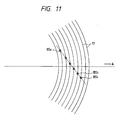
- Fig. 11 shows another embodiment of this invention, and a description will now be made of this embodiment, with the same reference numbers being placed on the same parts as in the above described embodiment.
- the system is set in such a way that the number of the laser beams is an even number, and, additionally, the spots of the individual laser beams are so arranged on the optical disk that the same numbers of the spots are positioned on both sides in relation to the axis of movement of the optical head.
- the laser diode 2 is provided with an even number of pieces of the laser diode elements 181 through 186 (six pieces in the Figure), as shown in Fig. 12, and the laser beams LB1 through LB6 emitted from the laser diode 2 are applied onto the optical disk 8 at the intervals l1 through l5 corresponding to the magnification of the image forming optical system 41 to form the beam spots BS1 through BS6, as shown in Fig. 11.
- the middle position of the two beam spots BS3 and BS4 in the middle is set to move in the radial direction A of the optical disk 8.
- the intervals of the individual beam spots BS1 through BS6 are set as shown below on the basis of Fig. 13. That is to say, the distance D m of the individual beam spots BS1 through BS6 is obtained by finding the crossing point of the equation for a circle expressing the tracks 17 and 17 ... and the equation for a straight line expressing the arrangement of the beam spots BS1 through BS6.
- the distance D m from the middle beam spot BS4 to the beam spot BS m in the m-th position either on the inner side or the outer side from the middle beam spot BS4 is calculated, and the intervals l1 through l5 of the individual beam spots BS1 through BS6 are obtained from this value as shown below.
- the radius of curvature R i is set at 30 mm
- the angle ⁇ is set at 87 degrees
- the pitch p is set at 1.6 ⁇ m.
- the tracking error signal for the performance of the tracking servo can be taken from either one of the two middle beams closest to the axis of movement of the optical head 40 or from the mean value of these.
- This invention consists in the construction and working described above, and, since the laser diode according to this invention is provided with a plurality of light emitting elements arranged at varying intervals, the laser diode is capable of irradiating all of the laser beams emitted from the plurality of light emitting elements onto the tracks on the optical writing media at the same time.
- the multibeam optical head according to this invention is so constructed as to be provided with a laser diode in which a plurality of independently drivable light emitting elements are arranged in a straight line with their intervals varied and an image forming optical system which forms images in such a manner that a plurality of beams from the laser diode mentioned above are applied onto the optical writing media to form images arranged linearly at a prescribed angle in relation to the radial direction of the optical writing media and additionally that the intervals of the plural number of beam spots are varied.
- the multibeam optical head according to this invention is capable of directing all the plural number of laser beams emitted from the laser diode onto the tracks of the optical writing media via the image forming optical system to form the images at the same time even when it is designed to form the images arranged linearly at a prescribed angle to the radial direction of the optical writing media at the same time by applying the laser beams.
Abstract
Description
- The present invention relates to a laser diode and a multibeam optical head using the the laser diode as used in an optical writing and reading system which optically performs writing, reading, erasure, and so forth of information by irradiating the convergent rays from a light source onto optical writing media.
- Along with the development of information processing systems in the recent years, it has been strongly desired that a high transfer data rate will be attained, in addition to the realization of a large capacity in the past, in optical writing and reading systems, so that the writing and reading of information may be accomplished thereby. Various efforts have been made towards this goal (as observed in 4p-ZD-1, 4p-ZD-2, etc. read at Extended Abstracts (The 49th Autum Meeting, 1989); The Japan Society of Applled Physics). In this regard, it has been proposed the adoption of multibeam in an optical head, which consists in using a plural number of writing and reading converging spots in an optical head, as a means of achieving a high transfer data rate just mentioned.
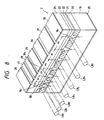
- An example of this type of multibeam optical head as proposed in the past is, for example, disclosed in Japanese Patent Laid Open No. 117744/1986. As shown in Fig. 14, the optical head is so constructed as to include a
laser diode array 100, in which many laser diodes independently controllable for their light emission are arranged linearly and at equal intervals to form a unified structure, acondenser lens 101, which converts the rays output from thelaser diode array 100 into parallel collimated rays, anobject lens 102, which converges the parallel rays mentioned above into minute spots, a polarizingbeam splitter 103, which separates the incident rays and the reflected rays, and a plurality of beam splitting and detecting means 104, which detects signals by splitting the reflected rays from a plurality of beam spots, a photo-detector 105, which detects the position of one track, and a pair of focusingerror detecting systems 106. - With this construction, it is made possible to perform the writing or reading of information on a plural number of
tracks 111 at the same time, by irradiating a plurality ofbeam spots 107 through 109 (three spots in the example shown in Fig. 15) onto a plural number oftracks 111 on anoptical disk 110 at the same time. - Now, in the case of the multibeam optical head mentioned above, if an attempt were made to arrange a plurality of
beam spots 107 through 109 linearly at equal intervals along a line in the radial direction A of theoptical disk 110, it would be necessary to set the spacing of the plurality of laser diodes arranged in the laser diode array very narrow, in consequence of such factors as the magnification of the optical system, so that it would virtually be impossible to manufacture thelaser diode array 100. Therefore, as shown in Fig. 17, a plurality ofbeam spots 112 through 120 arranged in a straight line are set at a slant by a prescribed angle ϑ in relation to the radial direction A of theoptical disk 110, so that the intervals of the plurality of laser diodes arranged in thelaser diode array 100 may thereby be set at a value feasible to the actual manufacture of the array. - However, the prior art described above has such problems as those mentioned below. That is to say, the multibeam optical head described above is designed to arrange a plurality of
beam spots 112 through 120 linearly at equal intervals, as shown Fig. 17. Therefore, if themany beam spots 112 through 120 were arranged in such a way as to be set at a slant at the angle ϑ in relation to the radial direction A of theoptical disk 110, as shown in Fig. 17, it would not be possible to position all of the plurality ofbeam spots 112 through 120 over thetracks 111 corresponding to these since thetracks 111 of theoptical disk 110 are formed in a circular arc having a prescribed radius of curvature, with the result that the beam spots on both ends would be positioned off thetracks 111. Consequently, it would not be possible to have all the beam spots perform the tracking of theirrespective tracks 111 at the same time and with accuracy even if tracking servo were applied to them, and this constitutes a problem in that the writing or reading of information could not be performed on a plurality oftracks 111 at the same time. - Therefore, the present invention has been made in order to overcome the above-mentioned problem of the prior art. An object of this invention is to provide a laser diode capable of tracking all the laser beams on all the individual tracks and performing the writing or reading of information on a plurality of tracks at the same time and a multibeam optical head using the laser diode, which performs writing or reading or the like at the same time, using a plurality of laser beams.
- That is to say, the laser diode according to the present invention is a laser diode for a multibeam optical head composed of a plurality of independently drivable light emitting diodes arranged in a straight line, wherein the plurality of light emitting spots are arranged at varying intervals.
- Moreover, the multibeam optical head according to the present invention is so constructed that it is provided with a laser diode wherein a plurality of independently drivable light emitting elements are arranged at varying intervals on a straight line and an image forming optical system which forms images by directing a plurality of beams from the laser diode mentioned above onto the optical writing media in such a way that a plurality of beam spots are arranged linearly at a prescribed angle to the radial direction of the writing media and that the intervals therebetween vary.
- As regards the manner of forming the images of the beam spots, one spot is positioned on the axis for the transit of the optical head in the radial direction of the optical writing media while the remaining spots are positioned in equal numbers on both sides of the transit axis, for the formation of images, in case the number of the beam spots is an odd number, for example.
- Also, in case the number of the beam spots mentioned above is an even number, the images are formed by positioning the beam spots in equal numbers on both sides of the transit axis, for example, in relation to the axis of the transit of the optical head in the radial direction of the optical writing media.
- However, the manner of image formation with the beam spots mentioned above is not limited to the image forming manners just described, but it is, of course, feasible to have the image formed with one beam spot positioned on the axis of transit for the optical head in the radial direction of the optical writing media and with the other beam spots being positioned on either one side of the axis of transit for the optical head.
- Moreover, for the error detection for tracking servo, it is desirable to obtain a basis therefor, for example, from the reflected rays of the spot positioned on the axis for the transit of the optical head in the radial direction of the optical writing media, in case the number of beam spots is an odd number, but from the reflected rays of the spot nearest to the axis for the transit of the optical head in the radial direction of the optical writing media in case the number of the beam spots is an even number.
- Furthermore, in order to separate the beam spot for the performance of the error detection for tracking servo out of a plurality of beam spots, a pin hole, for example, is used.
- In the laser diode according to this invention, a plurality of light emitting elements are arranged in a straight line with their intervals varied, and it is therefore possible to irradiate all the laser beams emitted from a plurality of light emitting elements on the tracks of all the optical writing media by arranging a plurality of light emitting elements with a variation by the prescribed amount, depending on the curvature of the tracks, even in case it is designed to irradiate the laser beams emitted from a plurality of light emitting elements over the tracks at the same time.
- Moreover, the multibeam optical head according to this invention is constructed in such a way as to be provided with a laser diode wherein a plurality of independently drivable light emitting elements are arranged at varying intervals in a straight line and with an image forming optical system which forms images by directing a plurality of beams from the laser diode mentioned above to the optical writing media in such a way as to arrange a plurality of beam spots linearly at a prescribed angle to the radial direction of the optical writing media and to vary the intervals therebetween, and the multibeam optical head is therefore capable of forming the images by focusing all of the plurality of laser beams emitted from the laser diode on the tracks on the optical writing media at the same time even in case all of the plurality of laser beams are irradiated at the same time to form the images arranged linearly at a prescribed angle to the radial direction of the optical writing media.
-
- Fig. 1 is a schematic construction view illustrating one embodiment in an optical writing and reading system to which a multibeam optical head according to this invention is applied;
- Fig. 2 and Fig. 3 are respectively a construction view and perspective view of the optical writing and reading system;
- Fig. 4 is a circuit diagram showing the detecting section for the tracking error signal;
- Fig. 5 is a perspective view showing the principle of the detection of the focusing error signal;
- Fig. 6 is a circuit diagram showing the detecting section for the focusing error signal;
- Figs. 7 (a), 7(b) and 7(c) are perspective views respectively showing the detecting operations for the focusing error signal;
- Fig. 8 is a perspective view showing the laser diode;
- Fig. 9 is a plane view showing the state of image formation with the multibeam;
- Fig. 10 is an explanatory view illustrating the method of setting the intervals of the multibeams;
- Fig. 11 is a plane view showing the state of image formation with this multibeam in illustration of another embodiment of this invention;
- Fig. 12 is a perspective view showing the laser diode;
- Fig. 13 is an explanatory view showing a method of setting the intervals of the multibeam;
- Fig. 14 is a perspective view showing a conventional multibeam optical head;
- Fig. 15 is a plane view illustrating the beam formed with the multibeam optical head shown in Fig. 14;
- Fig. 16 is an explanatory view showing one manner of image formation with the multibeams; and
- Fig. 17 is an explanatory chart showing another manner of image formation with the multibeams.
-
- Preferred embodiments of the present invention will now be described with reference to the accompanying drawings.
- Fig. 2 and Fig. 3 illustrate an optical writing and reading system to which a laser diode and a multibeam optical head both according to the present invention are applied.
- This optical writing and
reading system 1 is comprised of alaser diode 2, which is composed of a plurality of independently drivable light emitting elements arranged in a straight line, acollimator lens 3, which converts into parallel rays a plurality of the laser beams LB₁ through LB₇ (seven pieces in the Figures) having an elliptical sectional shape as emitted from thelaser diode 2, a beam shaping prism 4, which conditions into circular sectional shape the laser beams LB₁ through LB₇ as thus converted into parallel rays by thecollimator lens 3, a polarizingbeam splitter 5, which separates these shaped laser beams LB₁ through LB₇ between the rays irradiated to anoptical disk 8 to be mentioned later and the rays reflected from theoptical disk 8, a one-quarter wavelength plate 6, which converts the linear deflected rays and the circular deflected rays reciprocally from one into the other, anobject lens 7, which converges and irradiates the laser beams LB₁ through LB₇ having passed through the one-quarter wavelength plate 6 onto theoptical disk 8, theoptical disk 8 as the optical writing media onto which the laser beams LB₁ through LB₇ converged by theobject lens 7 are irradiated, abeam splitter 9, which further split into two parts the reflected laser beams LB₁ through LB₇ as separated by the polarizingbeam splitter 5 mentioned above, acondenser lens 10, which collects one part of the laser beams LB₁ through LB₇ as split by thebeam splitter 9, seven units ofphotodetector elements 11₁ through 11₇, which receive the part of the laser beams LB₁ through LB₇ as collected by thecondenser lens 10, acondenser lens 12, which collects the other part of the laser beams LB₁ through LB₇ as split by thebeam splitter 9 mentioned above, apinhole 13, which permits the passage of only the middle laser beam LB₄ among the laser beams LB₁ through LB₇ collected by thecondenser lens 12, acondenser lens 14 and acylindrical lens 15, which detect the focusing error signal by applying the astigmatic method to the laser beam LB₄ as taken out through thepinhole 13, and a photo-detector element 16, which receives the beam processed for image formation with thecondenser lens 14 and thecylindrical lens 15. - Also, the
optical disk 8 mentioned above has thetracks - Then, in the optical writing and reading system described above, a plurality of laser beams LB₁ through LB₇ which are emitted in an elliptical shape from the
laser diode 2 are converted into parallel rays with thecollimator lens 3 and thereafter shaped into circular beams by means of the beam shaping prism 4, as shown in Fig. 2. After that, these laser beams LB₁ through LB₇ pass through the polarizingbeam splitter 5 and the one-quarter wavelength plate 6, narrowed down with theobject lens 7 and irradiated on thetracks optical disk 8. - The rays reflected from the
tracks optical disk 8 mentioned above are fed back by the same route as what is mentioned above, and the rays are reflected by the polarizingbeam splitter 5 and at the same time split by thebeam splitter 9 for their transit in two directions. The laser beams LB₁ through LB₇ in one stream are applied by means of thecondenser lens 10 onto the seven photo-detector elements 11₁ through 11₇ to form images, and the image information recorded in a plurality oftracks detector elements 11₁ through 11₇. As shown in Fig. 4, the individual photo-detector elements 11₁ through 11₇ are connected with differential amplifiers, and image information is obtained asoutput signals 50₁ through 50₇ from the individual differential amplifiers. - Now, the laser beams LB₁ through LB₇ forming the other stream as split by the
beam splitter 9 mentioned above are condensed with acondenser lens 12, and thereafter only the middle laser beam LB₄ passes through thepinhole 13 and is applied to form its image onto the photo-detector element 16 by way of thecondenser lens 14 and thecylindrical lens 15. Thus, a tracking error signal is obtained, and also a focusing error signal is obtained by the astigmatic process. - The tracking error signal mentioned above is obtained in the manner described below. The photo-
detector element 16 is composed of mutually adjacent photo-detector elements photo receptor elements amplifiers amplifiers differential amplifier 56, and a tracking error signal is obtained from thisdifferential amplifier 56. - Also, the astigmatic process mentioned above, as already known, is constructed so as to obtain a focusing error signal through utilization of the feature that a circular beam is obtained in an approximately midway position in the in-focus state, as shown in Fig. 5, by varying the focus in the x-axis direction and that in the y-axis direction of the laser beam by means of the
cylindrical lens 15. The quadrantphoto receptor element 16 is provided with the photo-detector elements detector elements amplifiers differential amplifier 53, as shown in Fig. 6. - Now, the output from the differential amplifier becomes zero in the in-focus state as shown in Fig. 7 (a) whereas the output from the
differential amplifier 53 becomes either + or -, as shown in Figs. 7 (b) and 7(c), and a focusing error signal is thereby obtained. - In this regard, the laser diode in accordance with the embodiment is constructed with a plurality of light emitting elements mentioned above being arranged in a straight line at varying intervals. That is to say, the
laser diode 2 is provided, as shown in Fig. 1, with a plurality oflaser diode elements 18₁ through 18₇ arranged in one block in a straight line in such a way that the intervals X₁ through X₆ of the individual laser diode elements increase progressively (i.e. X₁ < X₂ ... < X₆). - The principal part of the
laser diode 2 mentioned above, as shown in Fig. 8, is composed of a p-GaAs substrate 19, an n-GaAs layer 20 formed on thesubstrate 19 and forming a current constricting layer, a p-Ga1-x AlxAslayer 21 formed on the n-GaAs layer 20 and forming a clad layer, a p-Ga1-yAlyAslayer 22 forming an active layer formed on the p-Ga1-xAlxAslayer 21, a p-Ga1-xAlxAslayer 23 forming a clad layer formed on the p-Ga1-yAlyAslayer 22, and an n-GaAs layer 24 forming a gap layer formed on the p-Ga1-xAlxAslayer 23. A p-side electrode 25 is formed over the entire area on the back side of the p-GaAs substrate, and, on the other hand, a plurality of n-side electrodes 26 through 32 are formed on the n-GaAs layer 24 mentioned above. Also, on the n-GaAs layer 20, which forms the current constricting layer mentioned above, are provided V-shaped grooves 33 through 39 formed by the mesa-etching process or the like, andlaser diode elements 18₁ through 18₇ are formed with the individual V-shaped grooves 33 through 39. - And, in an active area of the
individual laser elements 18₁ through 18₇, an electric current is injected from the direction indicated by the arrow into the inside region of the current constricting layer, n-GaAs layer 20, which has a polarity reverse to that of thesubstrate 19, through the V-shaped grooves 33 through 39 by applying a driving voltage independently between the p-side electrode 25 and the n-side electrode 26 through 32 mentioned above. Then, laser oscillation takes place in the p- Ga1-yAlyAslayer 22, which is the active layer, and a plurality of laser beams LB₁ through LB₇ each having an elliptical shape are obtained from the individuallaser diode elements 18₁ through 18₇. These laser beams LB₁ through LB₇ are emitted at intervals equal to the intervals X₁ through X₆ of thelaser diode elements 18₁ through 18₇. - Moreover, the multibeam optical head according to this embodiment is provided with a laser diode constructed as described above and an image forming optical system which directs the plural number of beams from the above-mentioned laser diode onto the optical writing media in such a way that a plurality of beam spots are arranged linearly at a prescribed angle in relation to the radial direction of the writing media and also the intervals therebetween vary.
- That is to say, the multibeam
optical head 40 is provided with an image formingoptical system 41, which is composed mainly of the component parts of the optical writing and reading system except for theoptical disk 8, in addition to thelaser diode 2, and thisoptical head 40, as shown in Fig. 2, is so constructed as to be capable of moving along the line in the radial direction A of theoptical disk 8 by the action of the driving means not shown in the Figure. - Now, a plurality of laser beams LB₁ through LB₇ emitted from the
laser diode 2 mentioned above are converged with theobject lens 7 through thecollimator lens 3, the anamorphic prism 4, thepolarizing beam splitter 5, and the one-quarter wavelength plate 6, as shown in Fig. 2, and directed in the form of a plurality of beam spots BS₁ through BS₇ onto theoptical disk 8 to form images thereon in a straight line with an angle ϑ in relation to the radial direction A of theoptical disk 8, as shown in Fig. 9. - Furthermore, the plural number of beam spots BS₁ through BS₇ irradiated in a straight line onto the
optical disk 8 mentioned above are, as shown in Fig. 1, are designed to perform their image formation with progressive increases of their intervals (i.e., l₁ < l₂ ... < l₆), so that all the beam spots will be positioned on thetracks optical disk 8. At this moment, the number of the beam spots BS₁ through BS₇ is seven, which is an odd number, and, among these beam spots BS₁ through BS₇, the middle beam spot BS₄ is so arranged as to move in the direction agreeing with the direction of movement of theoptical head 40, as shown in Fig. 9. - The intervals of these beam spots LB₁ through LB₇ are set as mentioned in the following part. First, as shown in Fig. 10, in case that the middle beam spot BS₄, among the beam spots BS₁ through BS₇ mentioned above, is arranged in such a way as to move along the line in the radial direction A of the
optical disk 8 and also to be positioned on thetrack 17 of theoptical disk 8, the beam spots are considered with being divided between inner side beam spots and outer side beam spots with respect to the beam spot BS₄. - First, the condition for the positioning of the beam spot BSm, which is in the m-th position on the inner side of the middle beam spot BS₄ mentioned above, on the
track 17m in the m-th position on the inner side of the track on which the middle beam spot BS₄ is positioned, is that the coordinates (x and y) of the beam spot BSm in the m-th position on the inner side should satisfy the equation for a circle expressive of thetrack 17m in the m-th position of the inner side as counted from the track where the middle beam spot BS₄ is positioned. Thus,
x² + y² = Ri² (1) - Where, Ri represents the radius of the
track 17m in the m-th position on the inner side. - Now, as shown in Fig. 10, the difference between the radius Ri of the
track 17m in the m-th position on the inner side and the X-coordinate of the beam spot BSm in the m-th position on the inner side is taken as Z while the distance from the middle beam spot BS₄ to the beam spot BSm in the m-th position on the inner side is taken as Dm, and then the equation (1) given above can be expressed as indicated in the following:
(R₁ - z)² + (Dm sin ϑ)² = Ri² (2) - Where, Z given above is expressed in the following equation as it is evident from Fig. 10.
Z = Dm cos ϑ - mp (3) - Where, p expresses the pitch of the
tracks
Dm² - 2Dm cos ϑ (mp + Ri) + (mp)² + 2mpRi = 0 (4) - Therefore, the distance Dm from the middle beam spot BS₄ to the beam spot BS m in the m-th position on the inner side is given by the following equation derived by solving the quadratic equation (4) given above:
Dm = cos ϑ (mp + Ri) + √R₁² - {sin [theta] (mp + Ri)}² (5) - In the meanwhile, Dm, which expresses the distance from the middle beam spot BS₄ mentioned above to the beam spot BSm in the m-th position on the outer side of the middle beam spot BS₄, is given by the following equation in the same manner as described above:
Dm = - Ri cos ϑ + √(Ri cos ϑ)² + (mp)² + 2Ri (mp) (6) - Therefore, the distance Dm from the middle beam spot BS₄ to the beam spot BSm in the m-th position either on the inner side or the outer side of the middle beam spot BS₄, with the equation (5) or the equation (6) given above being used therefor, and the intervals l₁ through l₆ of the individual beam spots BS₁ through BS₇ are obtained from this value as shown below. In this regard, the radius of curvature Ri is set at 30 mm, the angle ϑ is set at 87 degrees, and the pitch p is set at 1.6 µm. As the result, the intervals l₁ through l₆ for the individual beam spots BS₁ through BS₇ are found to be as shown in the following:
l₁ = 28.8 µm
l₂ = 29.0 µm
l₃ = 29.8 µm
l₄ = 30.4 µm
l₅ = 31.0 µm
l₆ = 32.3 µm - Therefore, in case a plurality of beam spots BS₁ through BS₇ are arranged in a straight line with a slant at the angle ϑ in relation to the radial direction A of the
optical disk 8, the intervals l₁ through l₆ of the beam spots BS₁ through BS₇ can be set at the value mentioned above in order to position all of the beam spots BS₁ through BS₇ on thetracks optical disk 8. - Moreover, the
laser diode 2, which emits the laser beam LB₁ through LB₇ mentioned above, has a plurality oflaser diode elements 18₁ through 18₇ arranged at the intervals x₁ through x₆, which reflects consideration given to the image forming magnification of the image formingoptical system 41, as shown in Fig. 1, so that the beam spots BS₁ through BS₇ are formed at the intervals l₁ through l₆ mentioned above. - In the construction described hereinabove, the multibeam head of the embodiment according to this invention performs, for example, the reproduction of information in the following manner. That is to say, in order to perform the reproduction of information, the
laser diode 2 emits a plurality of laser beams LB₁ through LB₇, as shown in Fig. 2, and these laser beams LB₁ through LB₇ are directed onto thetracks optical system 41 along a straight line set with a slant at the angle ϑ in relation to the radial direction A of theoptical disk 8 for their image formation as the beam spots BS₁ through BS₇. - The beam spots BS₁ through BS₇ formed on the
optical disk 8 mentioned above have their intervals l₁ through l₆ increasing gradually, so that all the beam spots BS₁ through BS₇ are positioned on thetracks optical disk 8. - Owing to this feature, it is possible in this embodiment to position all the laser beams LB₁ through LB₇ on the
tracks optical disk 8 at the same time and with accuracy even when it is attempted to attain a high transfer data rate in the reproduction of information from a plurality oftracks optical disk 8 at the same time by the use of a plurality of the laser beams LB₁ through LB₇. - In this embodiment, there are a plurality of laser beams, and it is best to detect the servo signal and particularly the tracking error signal for performing the tracking servo through the middle spot, in view of the fact that the difference in the radius of curvature between the
tracks - Fig. 11 shows another embodiment of this invention, and a description will now be made of this embodiment, with the same reference numbers being placed on the same parts as in the above described embodiment. In this embodiment, the system is set in such a way that the number of the laser beams is an even number, and, additionally, the spots of the individual laser beams are so arranged on the optical disk that the same numbers of the spots are positioned on both sides in relation to the axis of movement of the optical head.
- In specific terms, the
laser diode 2 is provided with an even number of pieces of thelaser diode elements 18₁ through 18₆ (six pieces in the Figure), as shown in Fig. 12, and the laser beams LB₁ through LB₆ emitted from thelaser diode 2 are applied onto theoptical disk 8 at the intervals l₁ through l₅ corresponding to the magnification of the image formingoptical system 41 to form the beam spots BS₁ through BS₆, as shown in Fig. 11. In this case, the middle position of the two beam spots BS₃ and BS₄ in the middle is set to move in the radial direction A of theoptical disk 8. - In this case, the intervals of the individual beam spots BS₁ through BS₆ are set as shown below on the basis of Fig. 13. That is to say, the distance Dm of the individual beam spots BS₁ through BS₆ is obtained by finding the crossing point of the equation for a circle expressing the
tracks - Accordingly, by the arithmetic operations performed as mentioned above, the distance Dm from the middle beam spot BS₄ to the beam spot BSm in the m-th position either on the inner side or the outer side from the middle beam spot BS₄ is calculated, and the intervals l₁ through l₅ of the individual beam spots BS₁ through BS₆ are obtained from this value as shown below. In this regard, the radius of curvature Ri is set at 30 mm, the angle ϑ is set at 87 degrees, and the pitch p is set at 1.6 µm. As the result, the intervals l₁ through l₅ of the individual beam spots BS₁ through BS₆ are given as follows:
l₁ = 29.5 µm
l₂ = 30.0 µm
l₃ = 30.0 µm
l₄ = 30.6 µm
l₅ = 31.2 µm - It is thus possible to position all of the beam spots BS₁ through BS₆ on the
tracks optical disk 8, as shown in Fig. 11, by setting the intervals l₁ through l₅ for the beam spots BS₁ through BS₆ at the values mentioned above, when a plurality of beam spots BS₁ through BS₆ are arranged in a straight line with a slant at the angle ϑ in relation to the radial direction A of theoptical disk 8. - Moreover, in case the number of the laser beams is thus an even number, there is no middle beam spot, unlike the case wherein the number of the laser beams is an odd number, but the tracking error signal for the performance of the tracking servo can be taken from either one of the two middle beams closest to the axis of movement of the
optical head 40 or from the mean value of these. - The construction and working of the other parts of the system in this embodiment are the same as those of the example of embodiment described above, and their description is therefore omitted here.
- This invention consists in the construction and working described above, and, since the laser diode according to this invention is provided with a plurality of light emitting elements arranged at varying intervals, the laser diode is capable of irradiating all of the laser beams emitted from the plurality of light emitting elements onto the tracks on the optical writing media at the same time.
- Moreover, the multibeam optical head according to this invention is so constructed as to be provided with a laser diode in which a plurality of independently drivable light emitting elements are arranged in a straight line with their intervals varied and an image forming optical system which forms images in such a manner that a plurality of beams from the laser diode mentioned above are applied onto the optical writing media to form images arranged linearly at a prescribed angle in relation to the radial direction of the optical writing media and additionally that the intervals of the plural number of beam spots are varied. Hence, the multibeam optical head according to this invention is capable of directing all the plural number of laser beams emitted from the laser diode onto the tracks of the optical writing media via the image forming optical system to form the images at the same time even when it is designed to form the images arranged linearly at a prescribed angle to the radial direction of the optical writing media at the same time by applying the laser beams.
Claims (2)
a laser diode including a plurality of independently drivable light emitting elements set in linear arrangement at varying intervals; and
an image forming optical system forming images on optical writing media with a plurality of beams from said laser diode, said images being a plurality of beam spots arranged in a line with a prescribed angle with respect to the radial direction of said optical writing media and intervals between the plurality of beam spots being varied.
Applications Claiming Priority (2)
| Application Number | Priority Date | Filing Date | Title |
|---|---|---|---|
| JP1059564A JPH081705B2 (en) | 1989-03-14 | 1989-03-14 | Semiconductor laser and multi-beam optical head using the same |
| JP59564/89 | 1989-03-14 |
Publications (2)
| Publication Number | Publication Date |
|---|---|
| EP0388760A1 true EP0388760A1 (en) | 1990-09-26 |
| EP0388760B1 EP0388760B1 (en) | 1995-08-02 |
Family
ID=13116861
Family Applications (1)
| Application Number | Title | Priority Date | Filing Date |
|---|---|---|---|
| EP90104710A Expired - Lifetime EP0388760B1 (en) | 1989-03-14 | 1990-03-13 | Laser diode and multibeam optical head using the laser diode |
Country Status (4)
| Country | Link |
|---|---|
| US (1) | US5144616A (en) |
| EP (1) | EP0388760B1 (en) |
| JP (1) | JPH081705B2 (en) |
| DE (1) | DE69021237T2 (en) |
Cited By (7)
| Publication number | Priority date | Publication date | Assignee | Title |
|---|---|---|---|---|
| EP0543505A1 (en) * | 1991-10-22 | 1993-05-26 | Canon Kabushiki Kaisha | Plural-beam optical head |
| EP0663662A2 (en) * | 1994-01-13 | 1995-07-19 | Toshinobu Futagawa | Optical head unit |
| US5619488A (en) * | 1991-09-07 | 1997-04-08 | Fuji Xerox Co., Ltd. | Information recording device |
| US5808986A (en) * | 1993-02-17 | 1998-09-15 | Vixel Corporation | Multiple beam optical memory system with solid-state lasers |
| WO1999042993A1 (en) * | 1998-02-20 | 1999-08-26 | Zen Research N.V. | Method and apparatus for reading multiple tracks and writing at least one track of an optical disk |
| US6229771B1 (en) | 1998-10-09 | 2001-05-08 | Zen Research (Ireland), Ltd. | Method and apparatus for generating focus error signals in a multi-beam optical disk drive |
| US6985414B2 (en) | 2001-01-08 | 2006-01-10 | Dragsholm Wireless Holdings Llc | Method and apparatus for writing on an optical disk with beam spots aligned at an angle to data tracks |
Families Citing this family (28)
| Publication number | Priority date | Publication date | Assignee | Title |
|---|---|---|---|---|
| JP3066118B2 (en) * | 1991-07-19 | 2000-07-17 | パイオニア株式会社 | Photodetector |
| JPH0696468A (en) * | 1992-09-14 | 1994-04-08 | Canon Inc | Optical recording and reproducing device and semiconductor laser array |
| US5526182A (en) * | 1993-02-17 | 1996-06-11 | Vixel Corporation | Multiple beam optical memory system |
| JPH07129966A (en) * | 1993-11-05 | 1995-05-19 | Matsushita Electric Ind Co Ltd | Multibeam optical head |
| JPH07147020A (en) * | 1993-11-24 | 1995-06-06 | Canon Inc | Plural beam optical head |
| US5523995A (en) * | 1994-04-01 | 1996-06-04 | Lichtenberg; Heinz D. | Optical information read/write system with a spread plane beam |
| GB2300749A (en) * | 1995-05-06 | 1996-11-13 | Thomson Multimedia Sa | A multiple beam optical disk system |
| JP3800653B2 (en) * | 1995-12-26 | 2006-07-26 | ソニー株式会社 | Crosstalk removal device |
| US5815482A (en) * | 1996-01-22 | 1998-09-29 | T Squared G, Inc. | Multibyte random access mass storage/memory system |
| US6038089A (en) | 1996-05-14 | 2000-03-14 | Asahi Kogaku Kogyo Kabushiki Kaisha | Beam shaping optical system |
| US6430125B1 (en) * | 1996-07-03 | 2002-08-06 | Zen Research (Ireland), Ltd. | Methods and apparatus for detecting and correcting magnification error in a multi-beam optical disk drive |
| US5959953A (en) * | 1996-07-03 | 1999-09-28 | Zen Research Nv | Methods and apparatus for performing cross-talk correction in a multi-track optical disk reader based on magnification error |
| US5870227A (en) * | 1997-03-13 | 1999-02-09 | T Squared G Systems, Inc. | Scanning head lens assembly |
| US6252715B1 (en) | 1997-03-13 | 2001-06-26 | T. Squared G, Inc. | Beam pattern contractor and focus element, method and apparatus |
| US20010050892A1 (en) * | 1997-07-11 | 2001-12-13 | Yoshitaka Takahashi | Optical disk apparatus compatible with different types of mediums |
| US5917797A (en) * | 1997-08-15 | 1999-06-29 | Zen Research Nv | Multi-beam optical pickup assembly and methods using a compact two-dimensional arrangement of beams |
| US6411573B1 (en) | 1998-02-20 | 2002-06-25 | Zen Research (Ireland), Ltd. | Multi-beam optical pickup |
| US6166756A (en) * | 1998-06-02 | 2000-12-26 | Science Applications International Corporation | Multiple channel data writing device |
| US6341118B1 (en) | 1998-06-02 | 2002-01-22 | Science Applications International Corporation | Multiple channel scanning device using oversampling and image processing to increase throughput |
| US6246658B1 (en) | 1998-06-02 | 2001-06-12 | Science Applications International Corporation | Multiple channel scanning device using optoelectronic switching |
| US6584052B1 (en) | 1998-06-02 | 2003-06-24 | Science Applications International Corporation | Method and apparatus for controlling the focus of a read/write head for an optical scanner |
| US6091067A (en) * | 1998-06-02 | 2000-07-18 | Science Applications International Corporation | Scanning device using fiber optic bimorph |
| US6137105A (en) * | 1998-06-02 | 2000-10-24 | Science Applications International Corporation | Multiple parallel source scanning device |
| US6137763A (en) * | 1998-09-24 | 2000-10-24 | Zen Research N.V. | Method and apparatus for buffering data in a multi-beam optical disk reader |
| US6700096B2 (en) * | 2001-10-30 | 2004-03-02 | Semiconductor Energy Laboratory Co., Ltd. | Laser apparatus, laser irradiation method, manufacturing method for semiconductor device, semiconductor device, production system for semiconductor device using the laser apparatus, and electronic equipment |
| US7105048B2 (en) * | 2001-11-30 | 2006-09-12 | Semiconductor Energy Laboratory Co., Ltd. | Laser irradiation apparatus |
| EP1997108A2 (en) * | 2006-03-10 | 2008-12-03 | Koninklijke Philips Electronics N.V. | Method and apparatus for writing/reading an information carrier and such an information carrier |
| CN113064136A (en) | 2020-01-02 | 2021-07-02 | 隆达电子股份有限公司 | Light emitting element and light emitting module |
Citations (2)
| Publication number | Priority date | Publication date | Assignee | Title |
|---|---|---|---|---|
| US4298974A (en) * | 1978-05-10 | 1981-11-03 | Hitachi, Ltd. | Optical head for a videodisc player/recorder |
| EP0092420A1 (en) * | 1982-04-19 | 1983-10-26 | Xerox Corporation | Information storage systems |
Family Cites Families (3)
| Publication number | Priority date | Publication date | Assignee | Title |
|---|---|---|---|---|
| US4594719A (en) * | 1984-01-19 | 1986-06-10 | Rca Corporation | Phase-locked laser array having a non-uniform spacing between lasing regions |
| JPS6311726U (en) * | 1986-07-09 | 1988-01-26 | ||
| JP2661098B2 (en) * | 1988-02-09 | 1997-10-08 | 日本電気株式会社 | Semiconductor laser and optical disk device |
-
1989
- 1989-03-14 JP JP1059564A patent/JPH081705B2/en not_active Expired - Fee Related
-
1990
- 1990-03-13 EP EP90104710A patent/EP0388760B1/en not_active Expired - Lifetime
- 1990-03-13 DE DE69021237T patent/DE69021237T2/en not_active Expired - Lifetime
- 1990-03-13 US US07/492,453 patent/US5144616A/en not_active Expired - Lifetime
Patent Citations (2)
| Publication number | Priority date | Publication date | Assignee | Title |
|---|---|---|---|---|
| US4298974A (en) * | 1978-05-10 | 1981-11-03 | Hitachi, Ltd. | Optical head for a videodisc player/recorder |
| EP0092420A1 (en) * | 1982-04-19 | 1983-10-26 | Xerox Corporation | Information storage systems |
Cited By (12)
| Publication number | Priority date | Publication date | Assignee | Title |
|---|---|---|---|---|
| US5619488A (en) * | 1991-09-07 | 1997-04-08 | Fuji Xerox Co., Ltd. | Information recording device |
| US5737300A (en) * | 1991-09-07 | 1998-04-07 | Fuji Xerox Co., Ltd. | Optical dish device |
| EP0543505A1 (en) * | 1991-10-22 | 1993-05-26 | Canon Kabushiki Kaisha | Plural-beam optical head |
| US5353274A (en) * | 1991-10-22 | 1994-10-04 | Canon Kabushiki Kaisha | Beam diameter expansion of a multi-beam optical information system |
| US5808986A (en) * | 1993-02-17 | 1998-09-15 | Vixel Corporation | Multiple beam optical memory system with solid-state lasers |
| EP0663662A2 (en) * | 1994-01-13 | 1995-07-19 | Toshinobu Futagawa | Optical head unit |
| EP0663662A3 (en) * | 1994-01-13 | 1995-08-09 | Futagawa Toshinobu | |
| WO1999042993A1 (en) * | 1998-02-20 | 1999-08-26 | Zen Research N.V. | Method and apparatus for reading multiple tracks and writing at least one track of an optical disk |
| US6314071B1 (en) | 1998-02-20 | 2001-11-06 | Zen Research (Ireland), Ltd. | Method and apparatus for reading multiple tracks and writing at least one track of an optical disk |
| US6229771B1 (en) | 1998-10-09 | 2001-05-08 | Zen Research (Ireland), Ltd. | Method and apparatus for generating focus error signals in a multi-beam optical disk drive |
| US6985414B2 (en) | 2001-01-08 | 2006-01-10 | Dragsholm Wireless Holdings Llc | Method and apparatus for writing on an optical disk with beam spots aligned at an angle to data tracks |
| US7403465B2 (en) | 2001-01-08 | 2008-07-22 | Dragsholm Wireless Holdings Llc | Method and apparatus for writing on an optical disk with beam spots aligned at an angle to data tracks |
Also Published As
| Publication number | Publication date |
|---|---|
| EP0388760B1 (en) | 1995-08-02 |
| DE69021237T2 (en) | 1996-05-02 |
| JPH02239436A (en) | 1990-09-21 |
| JPH081705B2 (en) | 1996-01-10 |
| DE69021237D1 (en) | 1995-09-07 |
| US5144616A (en) | 1992-09-01 |
Similar Documents
| Publication | Publication Date | Title |
|---|---|---|
| EP0388760B1 (en) | Laser diode and multibeam optical head using the laser diode | |
| US4817074A (en) | Method and apparatus for detecting the focusing state and positioning accuracy of a light beam directed onto an optical disk tracking guide in an optical recording system | |
| US4520472A (en) | Beam expansion and relay optics for laser diode array | |
| US4775968A (en) | Tracking error detecting system for optical head | |
| GB2288483A (en) | An opto-magnetic head aparatus | |
| US4520471A (en) | Multi-channel recording/playback optics for laser diode arrays | |
| US5835471A (en) | Optical information recording and/or reproducing apparatus | |
| US5270996A (en) | Optical head with diffraction grating producing five diffracted detection light beams | |
| US5579298A (en) | Optical scanner having symmetry about an oblique divider | |
| US5113378A (en) | Optical tracking system for an optical recording arrangement with plurality of beams | |
| JP3019181B2 (en) | Optical head servo signal detection device | |
| US7280453B2 (en) | Optical head and read/write drive including the optical head | |
| US5216562A (en) | Multi-beam optical recording system and method | |
| WO2000049605A1 (en) | Method of writing servo signal on magnetic tape | |
| US4888755A (en) | Optical head for recording informations into a record medium and reproducing the same therefrom | |
| US6567353B1 (en) | Optical head with light receiving element surfaces divided into at least three light receiving areas | |
| EP0390116B1 (en) | Optical information processing system | |
| US5107102A (en) | Arrangement for detecting a signal for effecting a focus control of an optical head | |
| JPH0721869B2 (en) | Optical pickup device | |
| CN1208223A (en) | Laser head device | |
| US5317557A (en) | Optical head for recording and reproducing information on and/or from optical record medium | |
| US5060214A (en) | Optical pickup device keeping coincident the optical axes of the objective lens and of the recording/reproducing beam | |
| EP0416283B1 (en) | Optical head with tracking error detecting system | |
| EP0478163B1 (en) | Multi-beam optical recording system and method | |
| JP2792157B2 (en) | Optical information recording / reproducing device |
Legal Events
| Date | Code | Title | Description |
|---|---|---|---|
| PUAI | Public reference made under article 153(3) epc to a published international application that has entered the european phase |
Free format text: ORIGINAL CODE: 0009012 |
|
| AK | Designated contracting states |
Kind code of ref document: A1 Designated state(s): DE FR GB NL |
|
| 17P | Request for examination filed |
Effective date: 19901129 |
|
| 17Q | First examination report despatched |
Effective date: 19930625 |
|
| GRAA | (expected) grant |
Free format text: ORIGINAL CODE: 0009210 |
|
| AK | Designated contracting states |
Kind code of ref document: B1 Designated state(s): DE FR GB NL |
|
| REF | Corresponds to: |
Ref document number: 69021237 Country of ref document: DE Date of ref document: 19950907 |
|
| ET | Fr: translation filed | ||
| PLBE | No opposition filed within time limit |
Free format text: ORIGINAL CODE: 0009261 |
|
| STAA | Information on the status of an ep patent application or granted ep patent |
Free format text: STATUS: NO OPPOSITION FILED WITHIN TIME LIMIT |
|
| 26N | No opposition filed | ||
| REG | Reference to a national code |
Ref country code: GB Ref legal event code: IF02 |
|
| PGFP | Annual fee paid to national office [announced via postgrant information from national office to epo] |
Ref country code: NL Payment date: 20090315 Year of fee payment: 20 |
|
| PGFP | Annual fee paid to national office [announced via postgrant information from national office to epo] |
Ref country code: GB Payment date: 20090311 Year of fee payment: 20 |
|
| PGFP | Annual fee paid to national office [announced via postgrant information from national office to epo] |
Ref country code: DE Payment date: 20090219 Year of fee payment: 20 |
|
| PGFP | Annual fee paid to national office [announced via postgrant information from national office to epo] |
Ref country code: FR Payment date: 20090101 Year of fee payment: 20 |
|
| REG | Reference to a national code |
Ref country code: NL Ref legal event code: V4 Effective date: 20100313 |
|
| REG | Reference to a national code |
Ref country code: GB Ref legal event code: PE20 Expiry date: 20100312 |
|
| PG25 | Lapsed in a contracting state [announced via postgrant information from national office to epo] |
Ref country code: GB Free format text: LAPSE BECAUSE OF EXPIRATION OF PROTECTION Effective date: 20100312 |
|
| PG25 | Lapsed in a contracting state [announced via postgrant information from national office to epo] |
Ref country code: NL Free format text: LAPSE BECAUSE OF EXPIRATION OF PROTECTION Effective date: 20100313 |
|
| PG25 | Lapsed in a contracting state [announced via postgrant information from national office to epo] |
Ref country code: DE Free format text: LAPSE BECAUSE OF EXPIRATION OF PROTECTION Effective date: 20100313 |