EP0381524B1 - Method of manufacturing transparent high density ceramic material - Google Patents
Method of manufacturing transparent high density ceramic material Download PDFInfo
- Publication number
- EP0381524B1 EP0381524B1 EP90301130A EP90301130A EP0381524B1 EP 0381524 B1 EP0381524 B1 EP 0381524B1 EP 90301130 A EP90301130 A EP 90301130A EP 90301130 A EP90301130 A EP 90301130A EP 0381524 B1 EP0381524 B1 EP 0381524B1
- Authority
- EP
- European Patent Office
- Prior art keywords
- high density
- ceramic material
- density ceramic
- transparent high
- thickness
- Prior art date
- Legal status (The legal status is an assumption and is not a legal conclusion. Google has not performed a legal analysis and makes no representation as to the accuracy of the status listed.)
- Expired - Lifetime
Links
Images

Classifications
-
- C—CHEMISTRY; METALLURGY
- C04—CEMENTS; CONCRETE; ARTIFICIAL STONE; CERAMICS; REFRACTORIES
- C04B—LIME, MAGNESIA; SLAG; CEMENTS; COMPOSITIONS THEREOF, e.g. MORTARS, CONCRETE OR LIKE BUILDING MATERIALS; ARTIFICIAL STONE; CERAMICS; REFRACTORIES; TREATMENT OF NATURAL STONE
- C04B35/00—Shaped ceramic products characterised by their composition; Ceramics compositions; Processing powders of inorganic compounds preparatory to the manufacturing of ceramic products
- C04B35/01—Shaped ceramic products characterised by their composition; Ceramics compositions; Processing powders of inorganic compounds preparatory to the manufacturing of ceramic products based on oxide ceramics
- C04B35/48—Shaped ceramic products characterised by their composition; Ceramics compositions; Processing powders of inorganic compounds preparatory to the manufacturing of ceramic products based on oxide ceramics based on zirconium or hafnium oxides, zirconates, zircon or hafnates
- C04B35/49—Shaped ceramic products characterised by their composition; Ceramics compositions; Processing powders of inorganic compounds preparatory to the manufacturing of ceramic products based on oxide ceramics based on zirconium or hafnium oxides, zirconates, zircon or hafnates containing also titanium oxides or titanates
- C04B35/491—Shaped ceramic products characterised by their composition; Ceramics compositions; Processing powders of inorganic compounds preparatory to the manufacturing of ceramic products based on oxide ceramics based on zirconium or hafnium oxides, zirconates, zircon or hafnates containing also titanium oxides or titanates based on lead zirconates and lead titanates, e.g. PZT
-
- C—CHEMISTRY; METALLURGY
- C04—CEMENTS; CONCRETE; ARTIFICIAL STONE; CERAMICS; REFRACTORIES
- C04B—LIME, MAGNESIA; SLAG; CEMENTS; COMPOSITIONS THEREOF, e.g. MORTARS, CONCRETE OR LIKE BUILDING MATERIALS; ARTIFICIAL STONE; CERAMICS; REFRACTORIES; TREATMENT OF NATURAL STONE
- C04B35/00—Shaped ceramic products characterised by their composition; Ceramics compositions; Processing powders of inorganic compounds preparatory to the manufacturing of ceramic products
- C04B35/622—Forming processes; Processing powders of inorganic compounds preparatory to the manufacturing of ceramic products
- C04B35/64—Burning or sintering processes
- C04B35/645—Pressure sintering
- C04B35/6455—Hot isostatic pressing
Definitions
- the present invention relates to a method of manufacturing a transparent, high density ceramic material containing oxides of Pb, La, Zr and Ti (hereinafter referred to as PLZT), and, in particular, to a manufacturing method which includes hot isostatic pressing of a sintered PLZT product.
- PLZT transparent, high density ceramic material containing oxides of Pb, La, Zr and Ti
- PLZT has been used for various optical devices, depending on the relative content of the Pb, La, Zr and Ti oxides, for example, optical modulation devices which utilize the Pockels effect, optical shutters and optical switches which utilize the Kerr effect, image memory devices which utilize the memory effect, as well as optical shutters which make use of the electro-optical scattering effect, image memories which make use of the surface electrostriction effect, memory devices which make use of the photochromic effect, image memory devices which make use of an optical ferroelectric effect, etc.
- HIP hot isostatic pressing method
- a high temperature and high pressure gas as a pressure medium
- HIP hot isostatic pressing method
- the applicant has previously proposed a method of manufacturing high density piezo ceramics such as PbTi3, PbNb2O6, PbTi x Zr y O3 + Nb2O5, etc, by using HIP (Japanese Patent Laid-Open Sho 58-182883).
- a transparent, high density ceramic material having high transparency and freedom from pores can be obtained by sintering PLZT in a vacuum up to 90% of the theoretical density and, further, applying HIP processing (Japanese Patent Laid-Open Sho 62-105955).
- sintering of PLZT has required a long time for obtaining the desired high transparency and, for example, it requires more than 60 hours for sintering under a normal pressure, requires more than 16 hours for a hot pressing method (hereinafter referred to as HP) conducted in an oxygen or reduced-pressure atmosphere, or more than 60 hours even in a multi-step sintering process comprising HP and sintering at a normal pressure or pressure reduction and normal temperature sintering.
- HP hot pressing method
- sintering conditions and HIP processing conditions, etc are also selected depending on the PLZT compositions.
- high light transmittance it requires at least 10 hours in total, that is, more than 5 hours for sintering at a normal pressure or in vacuum and more than 5 hours for HIP and, accordingly, improvement has been demanded also from an economical point of view and operationability.
- an object of the present invention to provide a method of efficiently manufacturing transparent, high density ceramic material that contains oxides of Pb, La, Zr and Ti.
- the present inventor has made a study on conditions for the PLZT composition, temperature in each of the steps and atmospheres with an aim of completing both the sintering and HIP processing each within 2 hours in order to more efficiently mass produce, on an industrial scale, a transparent, high density ceramic material having at least 65% light transmittance and, as a result, the present invention is based on the finding that the thickness of PLZT before applying the HIP processing contributes to the improvement of the transparency, as well as to the shortening of the sintering time and the HIP processing time.
- the present invention provides a process for producing transparent, high density ceramic material which comprises: sintering a green compact mainly comprising each oxide of lead, lanthanum, zirconium and titanium, in a vacuum from 133.33 x 10 ⁇ 2 to 133.33 x 10 ⁇ 5 Pa (1 x 10 ⁇ 2 to 1 x 10 ⁇ 5 Torr) within a range of temperature from 1150°C to 1250°C and a time from 0.5 to 2 hours, fabricating the thus sintered product into a thin sheet having a thickness of less than 1.5 mm, and embedding the thin sheet in a heat resistant vessel tightly charged with a powder with a grain size from 50»m to 3000 »m and comprising at least one of fused alumina, fused zirconia and fused magnesia and then applying an HIP processing using an inert gas as a pressure medium within a range of pressure from 500 to 700 kg/cm2, a temperature from 1050°C to 1200°C and a time from 0.5 to 2
- the sintering time and the HIP processing time can greatly be shortened as compared with the conventional method for obtaining transparent, high density PLZT having high light transmittance, in the present invention, excellent economical performance can be obtained due to energy saving and operationability due to the shortened time, and a ceramic material having extremely high transparency and density can be mass produced stably.
- the aimed optical transmittance of higher than 65% is obtained under the conditions of a final PLZT product having a thickness of 0.2 mm, with a measuring wavelength of 633 nm (helium-neon laser), under scattering light and including deflection loss.
- a green compact of the above composition is at first sintered into a product under vacuum of 133.33 x 10 ⁇ 2 - 133.33 x 10 ⁇ 5 Pa (1 x 10 ⁇ 2 - 1 x 10 ⁇ 5 Torr) at a temperature from 1150°C to 1250°C and within a time from 0.5 to 2 hours.
- Sintering in vacuum is necessary for preventing the formation of pores and intrusion of excess PbO during sintering, in which the vacuum degree, temperature range and processing time can be set as described below in view of to the effect obtainable by setting the thickness of the sintering product to less than 0.5 mm upon HIP processing.
- the thickness of the green compact which is to be sintered is not an important factor for obtaining the effect of shortening the time for sintering and HIP processing, it is preferably from 10 mm to 50 mm in view of the deformation upon sintering, fabricability subsequent steps, productivity, etc.
- the vacuum degree during sintering is preferably within a range from 133.33 x 10 ⁇ 2 to 133.33 x 10 ⁇ 5 Pa (1 x 10 ⁇ 2 - 1 x 10 ⁇ 5 Torr).
- the desired effect for preventing the formation of pores and invasion of excess PbO cannot be obtained with a vacuum degree of lower than 133.33 x 10 ⁇ 2 Pa (1 x 10 ⁇ 2 Torr) and, on the other hand, PLZT is discolored by reduction, thereby resulting in deterioration of the characteristics if the vacuum degree is higher than 133.33 x 10 ⁇ 5 Pa (1 x 10 ⁇ 5 Torr).
- the sintering temperature is set to a range of 1150°C to 1250°C depending on the composition of PLZT, desired property such as optical transmittance can be obtained within a short processing time of from 0.5 to 2 hours.
- Extension of the sintering time does not contribute to the improvement of the property, and it is not undesired in view of the economical property, as well as excess heating and long time sintering particularly results in evaporization of of PbO making the PLZT property unstable.
- HIP processing is applied to the resultant sintering product, which according to the invention, is fabricated into a thin sheet with a thickness of less than 1.5 mm.
- the thin-sheet sintered product is positioned in a heat resistant vessel embedded tightly packed with a powder having a grain size from 50 »m to 3000 »m and comprising at least one of fused alumina, fused zirconia and fused magnesia, and the HIP processing is then applied.
- the effect obtained by reducing the sintered product to a thin sheet having a thickness of less than 1.5 mm during HIP processing resides in the shortening of the sintering time and the HIP processing time as will be detailed in the subsequent example.
- the average grain size of the final product is about 0.5 »m to 5 »m and, in particular, a product with an average grain size of about 0.5 »m to 2 »m can be obtained by selecting an optimal condition.
- the average grain size of the final product exceeds 5 »m and, usually, is within a range of from about 10 »m to 20 »m. The present inventor has confirmed that the average grain size gives a great effect on the property of the optical shutter, etc.
- the present inventor has confirmed that the average grain size has to be reduced to less than 1/10 of the aperture of the optical shutter in order to satisfy demanded variation in the amount of light. Further, as the average grain size is reduced, the effect caused by chipping (detachment of particles) upon fabrication is reduced to facilitate fabrication.
- the thickness is preferably within a range from 0.2 mm to 1.5 mm and, particularly, from 0.3 mm to 1.0 mm.
- PLZT In the usage of PLZT described above, it is often used at a thickness of less than 1 mm and, particularly, it is desirable to apply the HIP processing after fabrication into a thickness nearly to that of the final product within the above-mentioned range in view of the productivity when taking the mirror finishing fabrication in the subsequent step, etc., into consideration.
- a heat resistant vessel for HIP processing is desirably made of such dense material that a pressure medium gas does not easily penetrate from the surface of the vessel, and a lid for the vessel is rendered slightly gas permeable so that air in the furnace is easily replaced with an atmospheric gas in the preparatory step for the processing.
- fused alumina, fused zirconia and fused magnesia are suitable since these fused (electro-molten) oxides are sufficiently chemically stable within the range of the processing temperature described above and comprise coarse crystal grains and their aggregated particle powder, sintering of the powder per se is not taken-place and they have preferred purity not to react easily with PLZT, etc.
- pores, etc. are not scarcely present at the inside of particles, they are not powderized after the pressing, can be used repeatedly and are easily available industrially.
- the particles have a grain size of greater than 50 »m.
- fused oxides of excessively great size are not desirable since voids are increased even if the particles are tightly charged in the vessel.
- the grain size of the coarse particle is about several millimeters, but the grain size is preferably less than 3000 »m since there is a difficulty in view of the operationability if the grain size is remarkably different.
- ceramic material of more stable property can be obtained by conducting vacuum sintering while embedding the green compact into the heat resistant vessel tightly charged with the powder as described above.
- a pressure medium gas at high temperature is required for HIP processing and, particularly, an inert gas is desirable.
- a small amount of an oxygen-containing Ar gas may be used in order to prevent evaporation of oxygen in the composition of PLZT.
- a desired property can be obtained by a processing time from 0.5 to 2 hours when setting the pressure to 500-700 kg/cm2 and the range of temperature from 1050°C to 1200°C in accordance with the range of PLZT composition.
- each of the sintering time under vacuum and the HIP processing time can be reduced to less than 1 hour by setting the thickness of the sintering product to less than 1 mm during HIP processing.
- PLZT of high transparency and high density having more stable property can be obtained by applying annealing in an oxygen atmosphere at 800°C to 1200°C for about 1 to 2 hours after the HIP processing.
- HIP processing was applied in a furnace using an Ar gas as a pressure medium under the processing temperature at 1150°C, pressure at 600 kg/cm2, for 1 hour.
- PLZT of high light transmittance of greater than 65% can be obtained even if each of the sintering time and the HIP time is about one hour and, particularly, high transmittance amounting to 69% can be obtained in this example.
- Example 2 the sintering time was controlled such that the light transmittance of each of the final products obtained from the thin sheet fabricated into a predetermined thickness was greater than 65% and the results are shown in Figure 2 where the thickness of the several samples during HIP is plotted against the sintering time required to obtain this level of light transmittance.
- Example 1 The green compact obtained in Example 1 was sintered under various vacuum degrees from 133.33 x 10 ⁇ 2 to 133.33 x 10 ⁇ 6 Pa (1 x 10 ⁇ 2 to 1 x 10 ⁇ 6 Torr) under the conditions of 1200°C x 1 hr.
- Example 3 After fabricating the resultant sintered products each into a thin sheet of 1 mm thickness, the same HIP processing as in Example 1 was applied and several transparent ceramic products having 0.2 mm thickness and applied with mirror polishing on both sides thereof were obtained after the processing. Light transmittance was measured by using a helium-neon laser at a wavelength of 633 nm (including reflection loss under the conditions described above). The results are shown in Figure 3.
- the sintering time was adjusted such that the light transmittance (with the thickness of 0.2 mm after applying mirror finishing to both sides) is greater than 65% in each of the final products, for the thickness of 0.5 mm and 10 mm during HIP processing and the average grain size of each final product was measured (sintering time of 1 hour and 20 hours respectively).
- the grain size was about 1 to 1.5 »m for the product having a thickness of 0.5 mm during HIP processing, while the average grain size was 20 to 30 »m for the product having a thickness of about 10 mm during HIP processing.
- These transparent high density ceramic materials were arranged in an optical shutter array used for optical printers with dot density of 600 DPI (shutter aperture of 30 »m) and, when the variation of the amount of light was measured under the same conditions, variation of the amount of light could be suppressed to less than 1/50 for the product having a thickness of 0.5 mm during HIP processing, whereas the variation the amount of light was as large about 1/20 for the product having 10 mm thickness during HIP processing, which could not satisfy the requirement at present.
Landscapes
- Chemical & Material Sciences (AREA)
- Engineering & Computer Science (AREA)
- Ceramic Engineering (AREA)
- Manufacturing & Machinery (AREA)
- Materials Engineering (AREA)
- Structural Engineering (AREA)
- Organic Chemistry (AREA)
- Composite Materials (AREA)
- Inorganic Chemistry (AREA)
- Compositions Of Oxide Ceramics (AREA)
Description
- The present invention relates to a method of manufacturing a transparent, high density ceramic material containing oxides of Pb, La, Zr and Ti (hereinafter referred to as PLZT), and, in particular, to a manufacturing method which includes hot isostatic pressing of a sintered PLZT product.
- PLZT has been used for various optical devices, depending on the relative content of the Pb, La, Zr and Ti oxides, for example, optical modulation devices which utilize the Pockels effect, optical shutters and optical switches which utilize the Kerr effect, image memory devices which utilize the memory effect, as well as optical shutters which make use of the electro-optical scattering effect, image memories which make use of the surface electrostriction effect, memory devices which make use of the photochromic effect, image memory devices which make use of an optical ferroelectric effect, etc.
- When PLZT is used as the transparent high density ceramic material, extremely high transparency is required in order to prevent scattering or absorption of light passing through the ceramic material.
- Accordingly, it is necessary to reduce pores in the inside of the PLZT attributable to the scattering of light and remove excess PbO, which causes the PLZT to turn yellow and absorb light.
- As a method of obtaining PLZT, there is known a so-called monoaxial pressing-type hot pressing method of charging a starting material powder for PLZT ceramic in a die made of aluminium oxide, silicon carbide, graphite, etc, and then pressing the powder by means of a punch made of alumina (US Patent No 3,666,666, 1972).
- In this method, however, there is a limit for the size of products obtained in view of the strength of the die, and punch at high temperature and uniform heating by using an external heater. Further, reaction between the punch or die material and the pressing product is inevitable and, furthermore, productivity is low.
- Meanwhile, as a method of manufacturing piezoelectric ceramics, a hot isostatic pressing method (hereinafter referred to as HIP) using a high temperature and high pressure gas as a pressure medium is known and the applicant has previously proposed a method of manufacturing high density piezo ceramics such as PbTi₃, PbNb₂O₆, PbTixZryO₃ + Nb₂O₅, etc, by using HIP (Japanese Patent Laid-Open Sho 58-182883).
- However, even if the above-mentioned method is applied to PLZT, it is difficult to completely remove pores formed at the inside of the PLZT and, particularly, it is impossible to remove large pores, thus making it difficult to attain high transparency and high density as is required for an optical device. Further, there is also known an atmospheric sintering method of sintering in a PbO-oxygen atmosphere as a method of removing large pores formed upon sintering PLZT. However, it is difficult to control the PbO vapor pressure. If the PbO vapor pressure is higher than a predetermined pressure, excess PbO intrudes to the inside of the PLZT, thus turning the PLZT into yellow. On the contrary, if the PbO pressure is low, the invasion of PbO can be prevented; however, pores in the inside of the PLZT can not be removed, thus the PLZT will not be stable.
- Furthermore, even a combination of the above-mentioned sintering method with HIP can not stably obtain transparent, high density ceramic material having the required high transparency and freedom from pores.
- In order to overcome such problems, the present inventor has already proposed that a transparent, high density ceramic material having high transparency and freedom from pores can be obtained by sintering PLZT in a vacuum up to 90% of the theoretical density and, further, applying HIP processing (Japanese Patent Laid-Open Sho 62-105955).
- Further, as the usage of PLZT has extended the demand for a further improvement in transparency and freedom from pores has increased, as has the desire to find a method of manufacturing the same with good productivity.
- Heretofore, sintering of PLZT has required a long time for obtaining the desired high transparency and, for example, it requires more than 60 hours for sintering under a normal pressure, requires more than 16 hours for a hot pressing method (hereinafter referred to as HP) conducted in an oxygen or reduced-pressure atmosphere, or more than 60 hours even in a multi-step sintering process comprising HP and sintering at a normal pressure or pressure reduction and normal temperature sintering.
- Further, in the technique proposed by the inventor described above, sintering conditions and HIP processing conditions, etc, are also selected depending on the PLZT compositions. However, for satisfying high light transmittance, it requires at least 10 hours in total, that is, more than 5 hours for sintering at a normal pressure or in vacuum and more than 5 hours for HIP and, accordingly, improvement has been demanded also from an economical point of view and operationability.
- It is, accordingly, an object of the present invention to provide a method of efficiently manufacturing transparent, high density ceramic material that contains oxides of Pb, La, Zr and Ti.
- The present inventor has made a study on conditions for the PLZT composition, temperature in each of the steps and atmospheres with an aim of completing both the sintering and HIP processing each within 2 hours in order to more efficiently mass produce, on an industrial scale, a transparent, high density ceramic material having at least 65% light transmittance and, as a result, the present invention is based on the finding that the thickness of PLZT before applying the HIP processing contributes to the improvement of the transparency, as well as to the shortening of the sintering time and the HIP processing time.
- That is, the present invention provides a process for producing transparent, high density ceramic material which comprises:
sintering a green compact mainly comprising each oxide of lead, lanthanum, zirconium and titanium,
in a vacuum from 133.33 x 10⁻² to 133.33 x 10⁻⁵ Pa (1 x 10⁻² to 1 x 10⁻⁵ Torr)
within a range of temperature from 1150°C to 1250°C and a time from 0.5 to 2 hours,
fabricating the thus sintered product into a thin sheet having a thickness of less than 1.5 mm, and
embedding the thin sheet in a heat resistant vessel tightly charged with a powder with a grain size from 50»m to 3000 »m and comprising at least one of fused alumina, fused zirconia and fused magnesia and then applying an HIP processing using an inert gas as a pressure medium within a range of pressure from 500 to 700 kg/cm², a temperature from 1050°C to 1200°C and a time from 0.5 to 2 hours. - With the production process according to the present invention, it is possible to prevent formation of pores and intrusion of excess PbO upon sintering and, further, the pores at the inside of PLZT can be reduced substantially to zero by the HIP processing.
- In particular, since the sintering time and the HIP processing time can greatly be shortened as compared with the conventional method for obtaining transparent, high density PLZT having high light transmittance, in the present invention, excellent economical performance can be obtained due to energy saving and operationability due to the shortened time, and a ceramic material having extremely high transparency and density can be mass produced stably.
- In the present invention, the aimed optical transmittance of higher than 65% is obtained under the conditions of a final PLZT product having a thickness of 0.2 mm, with a measuring wavelength of 633 nm (helium-neon laser), under scattering light and including deflection loss.
- These and other objects, as well as advantageous features of the present invention will become apparent by reading the following descriptions in conjuction with the accompanying drawings, wherein
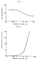
- Figure 1 is a graph illustrating a relationship between the thickness and the light transmittance of a specimen;
- Figure 2 is a graph illustrating a relationship between the thickness and the sintering time in vacuum; and
- Figure 3 is a graph illustrating a relationship between the vacuum degree and the light transmittance upon sintering.
- In the present invention, the composition for PLZT can properly be selected depending on the type of the optical devices, that is, in accordance with required electro-optical effect from the following ingredient composition:
(Pb1-xLax) (ZryToz) 1-x/4O₃ (1)
where
x = 0.05 - 0.25,
y/z = 0.05/0.95 - 0.95 - 0.05
which can be applied to any of the compositions with similar effect. - In the case of using the ceramic material, particularly, as an optical shutter array for optical printers, it is preferred to set the composition within a range:
x = 0.087 - 0.093
y/z = 0.66/0.34 - 0.64/0.36
in the above formula (1). - In the present invention, a green compact of the above composition is at first sintered into a product under vacuum of 133.33 x 10⁻² - 133.33 x 10⁻⁵ Pa (1 x 10⁻² - 1 x 10⁻⁵ Torr) at a temperature from 1150°C to 1250°C and within a time from 0.5 to 2 hours.
- Sintering in vacuum is necessary for preventing the formation of pores and intrusion of excess PbO during sintering, in which the vacuum degree, temperature range and processing time can be set as described below in view of to the effect obtainable by setting the thickness of the sintering product to less than 0.5 mm upon HIP processing.
- Further, although the thickness of the green compact which is to be sintered is not an important factor for obtaining the effect of shortening the time for sintering and HIP processing, it is preferably from 10 mm to 50 mm in view of the deformation upon sintering, fabricability subsequent steps, productivity, etc.
- The vacuum degree during sintering is preferably within a range from 133.33 x 10⁻² to 133.33 x 10⁻⁵ Pa (1 x 10⁻² - 1 x 10⁻⁵ Torr). The desired effect for preventing the formation of pores and invasion of excess PbO cannot be obtained with a vacuum degree of lower than 133.33 x 10⁻² Pa (1 x 10⁻² Torr) and, on the other hand, PLZT is discolored by reduction, thereby resulting in deterioration of the characteristics if the vacuum degree is higher than 133.33 x 10⁻⁵ Pa (1 x 10⁻⁵ Torr).
- After setting the vacuum degree within such a range, when the sintering temperature is set to a range of 1150°C to 1250°C depending on the composition of PLZT, desired property such as optical transmittance can be obtained within a short processing time of from 0.5 to 2 hours.
- Extension of the sintering time does not contribute to the improvement of the property, and it is not undesired in view of the economical property, as well as excess heating and long time sintering particularly results in evaporization of of PbO making the PLZT property unstable.
- Then, HIP processing is applied to the resultant sintering product, which according to the invention, is fabricated into a thin sheet with a thickness of less than 1.5 mm.
- The thin-sheet sintered product is positioned in a heat resistant vessel embedded tightly packed with a powder having a grain size from 50 »m to 3000 »m and comprising at least one of fused alumina, fused zirconia and fused magnesia, and the HIP processing is then applied.
- The effect obtained by reducing the sintered product to a thin sheet having a thickness of less than 1.5 mm during HIP processing, resides in the shortening of the sintering time and the HIP processing time as will be detailed in the subsequent example.
- When the transparency of the final product was investigated, it is found that sintering for a long time is required for obtaining a desired transmittance if the thickness of the sintering product during HIP processing exceeds 1.5 mm.
- In particular, grain growth of the sintered product can be suppressed by completing the sintering at a relatively low temperature and in a short period of time. In the manufacturing method according to the present invention, the average grain size of the final product is about 0.5 »m to 5 »m and, in particular, a product with an average grain size of about 0.5 »m to 2 »m can be obtained by selecting an optimal condition. In the conventional method described above, since sintering at high temperature and for a long time is inevitably necessary for obtaining a desired transparency, the average grain size of the final product exceeds 5 »m and, usually, is within a range of from about 10 »m to 20 »m. The present inventor has confirmed that the average grain size gives a great effect on the property of the optical shutter, etc. That is, in an optical shutter array, etc., used for optical printers, it is demanded to suppress the variation of the amount of light for each shutter to less than 1/50 for printing clear letters. As the dot density (number of dots per 1 inch) has been improved to 300 DPI, 600 DPI, etc, the aperture of the optical shutter has been reduced, for example to 60 »m, 30 »m, etc. Accordingly, if the average grain size of particles forming each of the optical shutters is large (the number of particles is small), the effect due to the variation of the electro-optical effect of individual particles is increased making it necessary to apply different voltages to the several optical shutters in order to decrease the variation of the amount of light. The present inventor has confirmed that the average grain size has to be reduced to less than 1/10 of the aperture of the optical shutter in order to satisfy demanded variation in the amount of light. Further, as the average grain size is reduced, the effect caused by chipping (detachment of particles) upon fabrication is reduced to facilitate fabrication.
- Further, in view of the fabrication of the sintered product to the thin sheet, handling thereof, etc, the thickness is preferably within a range from 0.2 mm to 1.5 mm and, particularly, from 0.3 mm to 1.0 mm.
- In the usage of PLZT described above, it is often used at a thickness of less than 1 mm and, particularly, it is desirable to apply the HIP processing after fabrication into a thickness nearly to that of the final product within the above-mentioned range in view of the productivity when taking the mirror finishing fabrication in the subsequent step, etc., into consideration.
- A heat resistant vessel for HIP processing is desirably made of such dense material that a pressure medium gas does not easily penetrate from the surface of the vessel, and a lid for the vessel is rendered slightly gas permeable so that air in the furnace is easily replaced with an atmospheric gas in the preparatory step for the processing. As the powder tightly packed in the heat resistant vessel, fused alumina, fused zirconia and fused magnesia are suitable since these fused (electro-molten) oxides are sufficiently chemically stable within the range of the processing temperature described above and comprise coarse crystal grains and their aggregated particle powder, sintering of the powder per se is not taken-place and they have preferred purity not to react easily with PLZT, etc.
- Further, since pores, etc., are not scarcely present at the inside of particles, they are not powderized after the pressing, can be used repeatedly and are easily available industrially.
- However, since sintering proceeds slowly even the fused oxides described above if they are fine powder, and it is necessary to prevent scattering during handling and to facilitate the replacing operation of air before pressing with a pressure medium gas, it is desirable that the particles have a grain size of greater than 50 »m.
- However, fused oxides of excessively great size are not desirable since voids are increased even if the particles are tightly charged in the vessel.
- Further, in the case of using fine powder and course powder by properly mixing them, it is theoretically possible that the grain size of the coarse particle is about several millimeters, but the grain size is preferably less than 3000 »m since there is a difficulty in view of the operationability if the grain size is remarkably different.
- In the present invention, ceramic material of more stable property can be obtained by conducting vacuum sintering while embedding the green compact into the heat resistant vessel tightly charged with the powder as described above.
- A pressure medium gas at high temperature is required for HIP processing and, particularly, an inert gas is desirable. A small amount of an oxygen-containing Ar gas may be used in order to prevent evaporation of oxygen in the composition of PLZT.
- Further, in view of the effect obtained by decreasing the thickness of the sintering product to less than 1.5 mm upon HIP processing, it is possible to set the pressure, the temperature range, and the processing time upon processing as described below.
- That is, it has been confirmed that a desired property can be obtained by a processing time from 0.5 to 2 hours when setting the pressure to 500-700 kg/cm² and the range of temperature from 1050°C to 1200°C in accordance with the range of PLZT composition. In particular, each of the sintering time under vacuum and the HIP processing time can be reduced to less than 1 hour by setting the thickness of the sintering product to less than 1 mm during HIP processing.
- Further, PLZT of high transparency and high density having more stable property can be obtained by applying annealing in an oxygen atmosphere at 800°C to 1200°C for about 1 to 2 hours after the HIP processing.
- Using a PLZT powder conditioned to a composition represented by the formula (1) described above in which x = 0.09, y = 0.65 and z = 0.35, a plurality of green compacts each size 60 mm x 50 mm (diameter x thickness) was obtained under a pressure of 3 t/cm².
- These green compacts were sintered under vacuum of 133.33 x 10⁻³ Pa(1 x 10⁻³ Torr) and under the conditions of 1200°C x 1 hr.
- After fabricating the thus obtained sintering product into thin sheets of various sizes ranging from 0.2 to 50 mm in thickness, they were embedded in an aluminium heat resistant vessel tightly charged with a fused zirconia powder with an average grain size of 300 »m, which was then loaded in a high temperature high pressure furnace.
- Then, HIP processing was applied in a furnace using an Ar gas as a pressure medium under the processing temperature at 1150°C, pressure at 600 kg/cm², for 1 hour.
- Then, from the sheets after the HIP processing, several transparent ceramic products having 0.2 mm thickness and mirror-polished on both surfaces thereof were obtained. The light transmittance was measured by using a helium-neon laser at a wavelength of 633 nm (including reflection loss under the foregoing conditions) and the results are shown in Figure 1, where the thickness of the several samples during HIP is plotted against light transmittance.
- As apparent from Figure 1, if the thickness of the sintered product (thin sheet) during HIP processing is less than 1.5 mm, PLZT of high light transmittance of greater than 65% can be obtained even if each of the sintering time and the HIP time is about one hour and, particularly, high transmittance amounting to 69% can be obtained in this example.
- When the density of PLZT with 1 mm thickness was measured, it was 7.80 g/cm³, and it was confirmed that the product has high density of 100% as compared with the theoretical density of 7.80 g/cm³.
- In the manufacturing method of Example 1, the sintering time was controlled such that the light transmittance of each of the final products obtained from the thin sheet fabricated into a predetermined thickness was greater than 65% and the results are shown in Figure 2 where the thickness of the several samples during HIP is plotted against the sintering time required to obtain this level of light transmittance.
- As apparent from Figure 2, if the thickness during HIP processing exceeds 1.5 mm, the sintering time becomes extremely long to require an extremely long time processing such as 7 hours for 5 mm thickness, more than 40 hours for the thickness greater than 20 mm. Thus, it has been confirmed that it is not suitable to industrial mass production when taking economical factor, operationability, etc into consideration.
- The green compact obtained in Example 1 was sintered under various vacuum degrees from 133.33 x 10⁻² to 133.33 x 10⁻⁶ Pa (1 x 10⁻² to 1 x 10⁻⁶ Torr) under the conditions of 1200°C x 1 hr.
- After fabricating the resultant sintered products each into a thin sheet of 1 mm thickness, the same HIP processing as in Example 1 was applied and several transparent ceramic products having 0.2 mm thickness and applied with mirror polishing on both sides thereof were obtained after the processing. Light transmittance was measured by using a helium-neon laser at a wavelength of 633 nm (including reflection loss under the conditions described above). The results are shown in Figure 3.
- As apparent from Figure 3, it can be seen that a vacuum degree of 133.33 x 10⁻² to 133.33 x 10⁻⁵ Pa (1 x 10⁻² to 1 x 10⁻⁵ Torr) is necessary during sintering in order to obtain highly transparent PLZT.
- In the manufacturing method of Example 1, the sintering time was adjusted such that the light transmittance (with the thickness of 0.2 mm after applying mirror finishing to both sides) is greater than 65% in each of the final products, for the thickness of 0.5 mm and 10 mm during HIP processing and the average grain size of each final product was measured (sintering time of 1 hour and 20 hours respectively).
- The grain size was about 1 to 1.5 »m for the product having a thickness of 0.5 mm during HIP processing, while the average grain size was 20 to 30 »m for the product having a thickness of about 10 mm during HIP processing. These transparent high density ceramic materials were arranged in an optical shutter array used for optical printers with dot density of 600 DPI (shutter aperture of 30 »m) and, when the variation of the amount of light was measured under the same conditions, variation of the amount of light could be suppressed to less than 1/50 for the product having a thickness of 0.5 mm during HIP processing, whereas the variation the amount of light was as large about 1/20 for the product having 10 mm thickness during HIP processing, which could not satisfy the requirement at present.
Claims (9)
- A method of manufacturing a transparent, high density ceramic material which comprises:
sintering a green compact mainly comprising an oxide of each of lead, lanthanum, zirconium and titanium in a vacuum from 133.33 x 10⁻² to 133.33 x 10⁻⁵ Pa (1 x 10⁻² to 1 x 10⁻⁵ Torr) within a temperature range of 1150°C to 1250°C and for a time from 0.5 to 2 hours to form a sintered product,
fabricating said sintered product into a thin sheet having a thickness of less than 1.5 mm,
positioning said thin sheet in a heat resistant vessel so that it is embedded in tightly packed powder with a grain size from 50 »m to 3000 »m comprising at least one of fused aluminium oxide, fused zirconium oxide and fused magnesium oxide and then
applying to said thin sheet hot isostatic pressing within a range of pressure from 49 to 68.7 MPa (500 to 700 kg/cm²), at a temperature from 1050°C to 1200°C and for a time from 0.5 to 2 hours by using an inert gas as a pressure medium. - A method of manufacturing a transparent high density ceramic material as defined in claim 1, wherein the thickness of the thin sheet which is hot isostatic pressed, is from 0.3 mm to 1.0 mm.
- A method of manufacturing a transparent high density ceramic material as defined in claim 1, wherein the thickness of the green compact which is sintered is from 10 mm to 50 mm.
- A method of manufacturing a transparent high density ceramic material as defined in claim 1, wherein annealing is applied in an oxygen atmosphere within a range of a temperature from 800 to 1200°C and for a time of from 1 to 2 hours after the hot isostatic pressing.
- A method of manufacturing a transparent high density ceramic material as defined in claim 1, wherein the green compact has the following ingredient composition:
(Pb1-x Lax) (ZryTiz) 1-x/4O₃
where
x = 0.087 - 0.093
y/z = 0.66/0.34 - 0.64/0.36. - A transparent high density ceramic material with light transmittance of higher than 65% prepared by the manufacturing method as defined in claim 1, wherein the optical transmittance is measured under the conditions of a thickness of 0.2 mm for transparent high density ceramic material, at a measuring wavelength of 633 nm (helium-neon laser), under scattered light and including reflection loss.
- A transparent high density ceramic material as defined in claim 6, wherein the average grain size is from 0.5»m to 5»m.
- A transparent high density ceramic material as defined in claim 6, wherein the average grain size is from 0.5»m to 2»m.
- An optical shutter array used for an optical printer, using the transparent high density magnetic material as defined in claim 6.
Applications Claiming Priority (2)
| Application Number | Priority Date | Filing Date | Title |
|---|---|---|---|
| JP25474/89 | 1989-02-02 | ||
| JP2547489 | 1989-02-02 |
Publications (3)
| Publication Number | Publication Date |
|---|---|
| EP0381524A2 EP0381524A2 (en) | 1990-08-08 |
| EP0381524A3 EP0381524A3 (en) | 1991-04-10 |
| EP0381524B1 true EP0381524B1 (en) | 1995-05-10 |
Family
ID=12167037
Family Applications (1)
| Application Number | Title | Priority Date | Filing Date |
|---|---|---|---|
| EP90301130A Expired - Lifetime EP0381524B1 (en) | 1989-02-02 | 1990-02-02 | Method of manufacturing transparent high density ceramic material |
Country Status (3)
| Country | Link |
|---|---|
| US (1) | US5032304A (en) |
| EP (1) | EP0381524B1 (en) |
| DE (1) | DE69019182T2 (en) |
Families Citing this family (49)
| Publication number | Priority date | Publication date | Assignee | Title |
|---|---|---|---|---|
| EP0667322B1 (en) * | 1993-09-02 | 2001-01-10 | Toto Ltd. | Light-permeable ceramic material and method of manufacturing the same |
| US5780377A (en) * | 1993-09-02 | 1998-07-14 | Toto Ltd. | Light-transmissive ceramics and method of manufacturing same |
| US5755234A (en) * | 1994-08-16 | 1998-05-26 | House Ear Institute | Pressure-regulating ear plug |
| US6232004B1 (en) * | 1998-05-06 | 2001-05-15 | Pacific Coast Technologies, Inc. | Methods for treating ceramic materials and improved treated ceramic materials produced thereby |
| US7682557B2 (en) | 2006-12-15 | 2010-03-23 | Smith International, Inc. | Multiple processes of high pressures and temperatures for sintered bodies |
| EP2658680B1 (en) | 2010-12-31 | 2020-12-09 | Saint-Gobain Ceramics & Plastics, Inc. | Abrasive articles comprising abrasive particles having particular shapes and methods of forming such articles |
| WO2013003830A2 (en) | 2011-06-30 | 2013-01-03 | Saint-Gobain Ceramics & Plastics, Inc. | Abrasive articles including abrasive particles of silicon nitride |
| WO2013003831A2 (en) | 2011-06-30 | 2013-01-03 | Saint-Gobain Ceramics & Plastics, Inc. | Liquid phase sintered silicon carbide abrasive particles |
| US9517546B2 (en) | 2011-09-26 | 2016-12-13 | Saint-Gobain Ceramics & Plastics, Inc. | Abrasive articles including abrasive particulate materials, coated abrasives using the abrasive particulate materials and methods of forming |
| KR20140106737A (en) | 2011-12-30 | 2014-09-03 | 생-고뱅 세라믹스 앤드 플라스틱스, 인코포레이티드 | Forming shaped abrasive particles |
| KR102074138B1 (en) | 2011-12-30 | 2020-02-07 | 생-고뱅 세라믹스 앤드 플라스틱스, 인코포레이티드 | Shaped abrasive particle and method of forming same |
| PL2797716T3 (en) | 2011-12-30 | 2021-07-05 | Saint-Gobain Ceramics & Plastics, Inc. | Composite shaped abrasive particles and method of forming same |
| US8840696B2 (en) | 2012-01-10 | 2014-09-23 | Saint-Gobain Ceramics & Plastics, Inc. | Abrasive particles having particular shapes and methods of forming such particles |
| EP2802436B1 (en) | 2012-01-10 | 2019-09-25 | Saint-Gobain Ceramics & Plastics, Inc. | Abrasive particles having complex shapes |
| WO2013149209A1 (en) | 2012-03-30 | 2013-10-03 | Saint-Gobain Abrasives, Inc. | Abrasive products having fibrillated fibers |
| KR101813466B1 (en) | 2012-05-23 | 2017-12-29 | 생-고뱅 세라믹스 앤드 플라스틱스, 인코포레이티드 | Shaped abrasive particles and methods of forming same |
| WO2014005120A1 (en) | 2012-06-29 | 2014-01-03 | Saint-Gobain Ceramics & Plastics, Inc. | Abrasive particles having particular shapes and methods of forming such particles |
| EP2906392B1 (en) | 2012-10-15 | 2025-04-16 | Saint-Gobain Abrasives, Inc. | Abrasive particles having particular shapes and methods of forming such particles |
| CN104994995B (en) | 2012-12-31 | 2018-12-14 | 圣戈本陶瓷及塑料股份有限公司 | Granular materials and forming method thereof |
| WO2014161001A1 (en) | 2013-03-29 | 2014-10-02 | Saint-Gobain Abrasives, Inc. | Abrasive particles having particular shapes and methods of forming such particles |
| TW201502263A (en) | 2013-06-28 | 2015-01-16 | Saint Gobain Ceramics | Abrasive article including shaped abrasive particles |
| CN111978921A (en) | 2013-09-30 | 2020-11-24 | 圣戈本陶瓷及塑料股份有限公司 | Shaped abrasive particles and methods of forming the same |
| KR102081045B1 (en) | 2013-12-31 | 2020-02-26 | 생-고뱅 어브레이시브즈, 인코포레이티드 | Abrasive article including shaped abrasive particles |
| US9771507B2 (en) | 2014-01-31 | 2017-09-26 | Saint-Gobain Ceramics & Plastics, Inc. | Shaped abrasive particle including dopant material and method of forming same |
| AU2015247739B2 (en) | 2014-04-14 | 2017-10-26 | Saint-Gobain Ceramics & Plastics, Inc. | Abrasive article including shaped abrasive particles |
| AU2015247826A1 (en) | 2014-04-14 | 2016-11-10 | Saint-Gobain Ceramics & Plastics, Inc. | Abrasive article including shaped abrasive particles |
| WO2015184355A1 (en) | 2014-05-30 | 2015-12-03 | Saint-Gobain Abrasives, Inc. | Method of using an abrasive article including shaped abrasive particles |
| US9914864B2 (en) | 2014-12-23 | 2018-03-13 | Saint-Gobain Ceramics & Plastics, Inc. | Shaped abrasive particles and method of forming same |
| US9707529B2 (en) | 2014-12-23 | 2017-07-18 | Saint-Gobain Ceramics & Plastics, Inc. | Composite shaped abrasive particles and method of forming same |
| US9676981B2 (en) | 2014-12-24 | 2017-06-13 | Saint-Gobain Ceramics & Plastics, Inc. | Shaped abrasive particle fractions and method of forming same |
| CN104557058B (en) * | 2014-12-24 | 2016-07-27 | 中国科学院上海硅酸盐研究所 | Vacuum-oxygen atmosphere is combined the method that hot pressed sintering prepares high permeability transparent electro-optic ceramics |
| TWI634200B (en) | 2015-03-31 | 2018-09-01 | 聖高拜磨料有限公司 | Fixed abrasive article and method of forming same |
| US10196551B2 (en) | 2015-03-31 | 2019-02-05 | Saint-Gobain Abrasives, Inc. | Fixed abrasive articles and methods of forming same |
| EP3307483B1 (en) | 2015-06-11 | 2020-06-17 | Saint-Gobain Ceramics&Plastics, Inc. | Abrasive article including shaped abrasive particles |
| JP6461833B2 (en) * | 2016-01-27 | 2019-01-30 | 信越化学工業株式会社 | Manufacturing method of transparent sintered body |
| KR102313436B1 (en) | 2016-05-10 | 2021-10-19 | 생-고뱅 세라믹스 앤드 플라스틱스, 인코포레이티드 | Abrasive particles and method of forming the same |
| EP4071224A3 (en) | 2016-05-10 | 2023-01-04 | Saint-Gobain Ceramics and Plastics, Inc. | Methods of forming abrasive articles |
| EP4349896A3 (en) | 2016-09-29 | 2024-06-12 | Saint-Gobain Abrasives, Inc. | Fixed abrasive articles and methods of forming same |
| US10759024B2 (en) | 2017-01-31 | 2020-09-01 | Saint-Gobain Ceramics & Plastics, Inc. | Abrasive article including shaped abrasive particles |
| US10563105B2 (en) | 2017-01-31 | 2020-02-18 | Saint-Gobain Ceramics & Plastics, Inc. | Abrasive article including shaped abrasive particles |
| CN110719946B (en) | 2017-06-21 | 2022-07-15 | 圣戈本陶瓷及塑料股份有限公司 | Particulate material and method of forming the same |
| US10928556B2 (en) * | 2019-05-24 | 2021-02-23 | Facebook Technologies, Llc | Optically transparent actuator |
| EP4081370A4 (en) | 2019-12-27 | 2024-04-24 | Saint-Gobain Ceramics & Plastics Inc. | Abrasive articles and methods of forming same |
| US11926019B2 (en) | 2019-12-27 | 2024-03-12 | Saint-Gobain Ceramics & Plastics, Inc. | Abrasive articles and methods of forming same |
| WO2021133876A1 (en) | 2019-12-27 | 2021-07-01 | Saint-Gobain Ceramics & Plastics, Inc. | Abrasive articles and methods of forming same |
| CN113929475A (en) * | 2021-11-03 | 2022-01-14 | 中科听海(苏州)电子科技有限责任公司 | Method for preparing piezoelectric ceramic based on hot isostatic pressing process |
| MX2024007593A (en) | 2021-12-30 | 2024-08-20 | Saint Gobain Abrasives Inc | Abrasive articles and methods of forming same. |
| CN118591436A (en) | 2021-12-30 | 2024-09-03 | 圣戈班磨料磨具有限公司 | Abrasive article and method of forming the same |
| EP4457054A4 (en) | 2021-12-30 | 2026-01-14 | Saint Gobain Abrasives Inc | Grinding articles and methods for shaping them |
Family Cites Families (3)
| Publication number | Priority date | Publication date | Assignee | Title |
|---|---|---|---|---|
| US3666666A (en) * | 1969-12-17 | 1972-05-30 | Atomic Energy Commission | Ferroelectric ceramic materials |
| US3718723A (en) * | 1970-10-23 | 1973-02-27 | Bell Telephone Labor Inc | Use of water soluble lanthanum compounds in lead zirconate-lead titanate ceramics |
| US3917780A (en) * | 1973-08-09 | 1975-11-04 | Us Air Force | Preparation of lead lanthanum zirconate titanate bodies |
-
1990
- 1990-02-02 EP EP90301130A patent/EP0381524B1/en not_active Expired - Lifetime
- 1990-02-02 US US07/474,340 patent/US5032304A/en not_active Expired - Lifetime
- 1990-02-02 DE DE69019182T patent/DE69019182T2/en not_active Expired - Lifetime
Also Published As
| Publication number | Publication date |
|---|---|
| EP0381524A3 (en) | 1991-04-10 |
| EP0381524A2 (en) | 1990-08-08 |
| US5032304A (en) | 1991-07-16 |
| DE69019182D1 (en) | 1995-06-14 |
| DE69019182T2 (en) | 1995-11-23 |
Similar Documents
| Publication | Publication Date | Title |
|---|---|---|
| US5032304A (en) | Method of manufacturing transparent high density ceramic material | |
| US8329605B2 (en) | Sintered product with a cubic structure | |
| EP2500332B1 (en) | Cubic boron nitride sintered compact, coated cubic boron nitride sintered compact, method for producing cubic boron nitride sintered compact, and method for producing coated cubic boron nitride sintered compact | |
| US5112433A (en) | Process for producing sub-micron ceramic powders of perovskite compounds with controlled stoichiometry and particle size | |
| JP6724266B2 (en) | Potassium sodium niobate sputtering target and manufacturing method thereof | |
| EP0563758B1 (en) | Preparation of sintered zirconia body | |
| DE68915146T2 (en) | MOLDING FORMING OPTICAL PARTS AND METHOD FOR PRODUCING IT. | |
| EP2505694A2 (en) | Method for solid-sate single crystal growth | |
| US10003009B2 (en) | Composite piezoelectric ceramic and piezoelectric device | |
| JP3399785B2 (en) | Piezoelectric device and method of manufacturing the same | |
| US5106794A (en) | Zirconium oxide sinter for forming thin film thereof and method for production of the same | |
| JP4582835B2 (en) | Method for manufacturing piezoelectric member for actuator | |
| KR101722391B1 (en) | Method of forming lead zirconate titanate sintered compact, lead zirconate titanate sintered compact and lead zirconate titanate sputtering target | |
| JP2632508B2 (en) | Transparent high density porcelain | |
| JPWO2005047206A1 (en) | Material exhibiting negative or low thermal expansion coefficient and method for producing the same | |
| JPH0818872B2 (en) | Manufacturing method of transparent high density porcelain | |
| US20060290240A1 (en) | Piezoelectric/electrostrictive porcelain composition, piezoelectric/electrostrictive body, and piezoelectric/electrostrictive film type device | |
| US6432353B1 (en) | Method for producing oxide type ceramic sintered body | |
| KR100294850B1 (en) | Manufacturing Method of PZT Thick Film Using Partially Melted Material | |
| EP1457469A1 (en) | Piezoelectric-electrostrictive material and its production method | |
| JP2020142950A (en) | Heat treatment member composed of zirconia sintered body | |
| JPH022824B2 (en) | ||
| JP3236641B2 (en) | Manufacturing method of composite ferroelectric ceramics | |
| JP2985350B2 (en) | Method for producing lead-based composite oxide using phase transition method | |
| JPS63236756A (en) | Polycrystal artificial ruby and manufacture |
Legal Events
| Date | Code | Title | Description |
|---|---|---|---|
| PUAI | Public reference made under article 153(3) epc to a published international application that has entered the european phase |
Free format text: ORIGINAL CODE: 0009012 |
|
| AK | Designated contracting states |
Kind code of ref document: A2 Designated state(s): DE NL |
|
| PUAL | Search report despatched |
Free format text: ORIGINAL CODE: 0009013 |
|
| RHK1 | Main classification (correction) |
Ipc: C04B 35/46 |
|
| AK | Designated contracting states |
Kind code of ref document: A3 Designated state(s): DE NL |
|
| 17P | Request for examination filed |
Effective date: 19910930 |
|
| 17Q | First examination report despatched |
Effective date: 19930402 |
|
| RAP1 | Party data changed (applicant data changed or rights of an application transferred) |
Owner name: SUMITOMO SPECIAL METALS COMPANY LIMITED |
|
| GRAA | (expected) grant |
Free format text: ORIGINAL CODE: 0009210 |
|
| AK | Designated contracting states |
Kind code of ref document: B1 Designated state(s): DE NL |
|
| REF | Corresponds to: |
Ref document number: 69019182 Country of ref document: DE Date of ref document: 19950614 |
|
| PLBE | No opposition filed within time limit |
Free format text: ORIGINAL CODE: 0009261 |
|
| STAA | Information on the status of an ep patent application or granted ep patent |
Free format text: STATUS: NO OPPOSITION FILED WITHIN TIME LIMIT |
|
| 26N | No opposition filed | ||
| PGFP | Annual fee paid to national office [announced via postgrant information from national office to epo] |
Ref country code: NL Payment date: 20090220 Year of fee payment: 20 Ref country code: DE Payment date: 20090306 Year of fee payment: 20 |
|
| NLV7 | Nl: ceased due to reaching the maximum lifetime of a patent |
Effective date: 20100202 |
|
| PG25 | Lapsed in a contracting state [announced via postgrant information from national office to epo] |
Ref country code: DE Free format text: LAPSE BECAUSE OF EXPIRATION OF PROTECTION Effective date: 20100202 |