EP0380964B1 - Method of making a semiconductor device having a contact member - Google Patents
Method of making a semiconductor device having a contact member Download PDFInfo
- Publication number
- EP0380964B1 EP0380964B1 EP90100909A EP90100909A EP0380964B1 EP 0380964 B1 EP0380964 B1 EP 0380964B1 EP 90100909 A EP90100909 A EP 90100909A EP 90100909 A EP90100909 A EP 90100909A EP 0380964 B1 EP0380964 B1 EP 0380964B1
- Authority
- EP
- European Patent Office
- Prior art keywords
- conductivity type
- layer
- electrically conductive
- semiconductor substrate
- region
- Prior art date
- Legal status (The legal status is an assumption and is not a legal conclusion. Google has not performed a legal analysis and makes no representation as to the accuracy of the status listed.)
- Expired - Lifetime
Links
Images

Classifications
-
- H—ELECTRICITY
- H01—ELECTRIC ELEMENTS
- H01L—SEMICONDUCTOR DEVICES NOT COVERED BY CLASS H10
- H01L23/00—Details of semiconductor or other solid state devices
- H01L23/48—Arrangements for conducting electric current to or from the solid state body in operation, e.g. leads, terminal arrangements ; Selection of materials therefor
- H01L23/482—Arrangements for conducting electric current to or from the solid state body in operation, e.g. leads, terminal arrangements ; Selection of materials therefor consisting of lead-in layers inseparably applied to the semiconductor body
- H01L23/485—Arrangements for conducting electric current to or from the solid state body in operation, e.g. leads, terminal arrangements ; Selection of materials therefor consisting of lead-in layers inseparably applied to the semiconductor body consisting of layered constructions comprising conductive layers and insulating layers, e.g. planar contacts
-
- H—ELECTRICITY
- H01—ELECTRIC ELEMENTS
- H01L—SEMICONDUCTOR DEVICES NOT COVERED BY CLASS H10
- H01L21/00—Processes or apparatus adapted for the manufacture or treatment of semiconductor or solid state devices or of parts thereof
- H01L21/02—Manufacture or treatment of semiconductor devices or of parts thereof
- H01L21/04—Manufacture or treatment of semiconductor devices or of parts thereof the devices having at least one potential-jump barrier or surface barrier, e.g. PN junction, depletion layer or carrier concentration layer
- H01L21/18—Manufacture or treatment of semiconductor devices or of parts thereof the devices having at least one potential-jump barrier or surface barrier, e.g. PN junction, depletion layer or carrier concentration layer the devices having semiconductor bodies comprising elements of Group IV of the Periodic System or AIIIBV compounds with or without impurities, e.g. doping materials
- H01L21/28—Manufacture of electrodes on semiconductor bodies using processes or apparatus not provided for in groups H01L21/20 - H01L21/268
- H01L21/283—Deposition of conductive or insulating materials for electrodes conducting electric current
- H01L21/285—Deposition of conductive or insulating materials for electrodes conducting electric current from a gas or vapour, e.g. condensation
- H01L21/28506—Deposition of conductive or insulating materials for electrodes conducting electric current from a gas or vapour, e.g. condensation of conductive layers
- H01L21/28512—Deposition of conductive or insulating materials for electrodes conducting electric current from a gas or vapour, e.g. condensation of conductive layers on semiconductor bodies comprising elements of Group IV of the Periodic System
- H01L21/28525—Deposition of conductive or insulating materials for electrodes conducting electric current from a gas or vapour, e.g. condensation of conductive layers on semiconductor bodies comprising elements of Group IV of the Periodic System the conductive layers comprising semiconducting material
-
- H—ELECTRICITY
- H01—ELECTRIC ELEMENTS
- H01L—SEMICONDUCTOR DEVICES NOT COVERED BY CLASS H10
- H01L2924/00—Indexing scheme for arrangements or methods for connecting or disconnecting semiconductor or solid-state bodies as covered by H01L24/00
- H01L2924/0001—Technical content checked by a classifier
- H01L2924/0002—Not covered by any one of groups H01L24/00, H01L24/00 and H01L2224/00
Definitions
- This invention relates to a fabrication method of semiconductor devices, for example, to static RAMs (Random Access Memories).
- a field oxide film 2 for element separation is grown on a P type silicon substrate 1 by a well-known LOCOS (Local Oxidation of Silicon) method, and then a gate oxide film 3 is formed by thermal oxidation.
- LOCOS Local Oxidation of Silicon
- the gate oxide film 3 in a predetermined area is etched away as shown in Figure 5C (this forms a predetermined contact part 4).
- a polysilicon layer 5 is deposited on the entire face including the contact part 4 by a well-known CVD (Chemical Vapor Deposition) method; and the polysilicon layer 5 is doped by, for example, phosphorus or the like to be N type; and then after a predetermined area is covered by a photoresist 40, a pattern is defined by, for example, a dry etching in order to leave only a predetermined polysilicon layer 5a (wiring layer) and 5b (gate electrode) as shown in Figure 5E. At this time, the P type silicon substrate 1 is also etched by patterning to form a recessed part 4a as shown in the figure.
- CVD Chemical Vapor Deposition
- the recessed part 4a in the figure is exaggerated to facilitate the understanding as said in the above.
- 4b in the figure is a connecting region of the polysilicon layer 5a and the P type silicon substrate 1 (that is, an N + type diffusion region which will be described later).
- the gate oxide film 3 in a predetermined region is etched away except directly below the polysilicon layer 5b, using the above photoresist 40.
- a predetermined area is selectively ion implanted with an N type impurity (for example As) 50 and is annealed (thermal treatment) to form N + type diffusion region 6 and 7 (source region and drain region) as shown in Figure 5G; and furthermore, an interlevel insulating layer 8 (a phosphorus glass film such as, for example, PSG (Phosphosilicate Glass) or BPSG (Borophosphosilicate Glass)) is deposited as shown in Figure 5H.
- N type impurity for example As
- BPSG Biophosphosilicate Glass
- a purpose of the invention is to provide semiconductor devices which are highly reliable and permit high degree of integration, and a fabrication method thereof.
- Figures 1 - 3 show an embodiment in which the invention is applied to a static RAM.
- N + type source region 6 and an N + type drain region 7 are formed in a predetermined pattern in a major surface of a P type silicon substrate 1; a gate electrode 5b is provided therebetween through a gate oxide film 3; and an N channel MOS transistor (for example, a transistor Q 4 in Figure 2) is structured.
- a wiring layer 5a of a predetermined pattern (for example, this wiring layer 5a is connected to a gate of an N channel MOS transistor Q 1 in Figure 2) is formed on the gate oxide film 3 and a field oxide film 2 formed on the P type silicon substrate 1; an N + type diffusion region 10 is formed by self-diffusion under a contact hole 9 formed in an adjacent region 12 of the wiring layer 5a; and this N + type diffusion region 10 is connected to the source region 6.
- a polysilicon layer 11 (conductive layer) is deposited into the contact hole 9, in a state of connection to the wiring layer 5a. 13 in the figure is a groove.
- Figure 2 is an equivalent circuit diagram showing an example of the static MOS memory.
- Q 1 - Q 6 in Figure 2 are N channel MOS transistors respectively.
- a device of the invention includes the wiring layer 5a of the predetermined pattern formed through the gate oxide film 3, the N + type diffusion layer formed under the contact hole 9 formed in the gate oxide film 3 in the adjacent region 12 of the wiring layer 5a, and the polysilicon layer 11 deposited into the contact hole 9 in a state of connection to the wiring layer 5a, so that the area of a region (the gate oxide film 3 under the wiring layer 5a and the adjacent region 12 of the wiring layer 5a in Figure 1), which corresponds to the contact part 4 (the connecting region 4b and a region of the recess part 4a) in a device by the conventional direct contact method as shown in Figure 5, can be reduced.
- the connection characteristic may be sufficiently secured in this part. Therefore, the gate oxide film 3 under the wiring layer 5a may be smaller (however, this gate oxide film 3 may not entirely removed), so that the area of the above wiring layer 5a and the gate oxide film 3 may be reduced. Also, because the connection to the N + type diffusion region (source region) 6 is made by the self-diffusion of the polysilicon layer 11 buried in the contact hole 9 (that is, by the N + type diffusion region 10), there is little need to consider an excess area by, for example, alignment difference or the like, which is very advantageous to reduction of the device size. Thus, the defects in the direct contact method may be solved, and the high degree of integration of the device is made possible, taking advantage of its characteristic.
- a field oxide film 2 (for example, 8000 ⁇ thick) is grown on a P type silicon substrate 1 by a well-known LOCOS method, and then a gate oxide film 3 (for example, 200 ⁇ thick) is formed on the silicon substrate 1 by thermal oxidation.
- a polysilicon layer 5 (for example 5000 ⁇ thick) is deposited over the entire face by a well-known, for example, low pressure CVD method; then phosphorus, for example, is deposited by a CVD method at 950 degrees centigrade; and a thermal treatment is performed to dope the polysilicon layer 5 to be an N type.
- a predetermined pattern is defined by, for example, dry etching to form a wiring layer 5a and a gate electrode 5b.
- ion 60 of an N type impurity (for example As) is selectively implanted by a well-known ion implantation method, and an annealing is performed at 950 degrees centigrade to form the N + type diffusion region 6 and 7 (source region and drain region).
- an interlevel insulating layer 8 (for example, BPSG or the like) is deposited over the entire face by, for example, a normal pressure CVD method, and a steam treatment is performed at 850 degrees centigrade to planarize the interlevel insulating layer 8 and to increase the degree of oxidation (insulation).
- a predetermined area is covered with a mask (for example, photoresist, not shown); then a groove 13 is formed by, for example, a dry etching of the interlevel insulating layer 8 in a predetermined area; and a contact hole 9 is formed by etching away the polysilicon layer 5a and removing the gate oxide film 3 by a predetermined dry etching as shown in Figure 3G.
- a mask for example, photoresist, not shown
- a polysilicon layer 11 is deposited by a well-known decreased pressure CVD method over the entire face which includes the contact hole 9 and the groove 13, and the polysilicon layer 11 is made low resistance by annealing at 900 degrees centigrade.
- an N + type diffusion region 10 is formed by self-diffusion under the contact hole 9 to be connected to the source region 6. This connects the polysilicon layer 11 and the wiring layer 5a.
- one process may be omitted by performing the deposition of the polysilicon layer 11 and the anneal at the same step, which is advantageous.
- a layer of SiO 2 (for example, 3000 ⁇ thick) is again deposited by, for example, a well-known decreased pressure CVD method, and each normal wiring treatment is performed to complete the device.
- the device of the embodiment and the fabrication method thereof do not require a mask process which removes the gate oxide film 3 in the predetermined region as in the conventional direct contact method shown in Figure 5B, the reliability of the device may be secured without contamination of the gate oxide film 3. Also, because a cleaning process for the contaminated gate oxide film 3 is not required as in conventional processes, it is an advantageous process without increased number of steps.
- the P type silicon substrate 1 would not be exposed by alignment difference of the mask or the like as in the patterning of the polysilicon layer 5 shown in Figure 5E (because of the gate oxide film 3 as shown in Figure 3C), the P type silicon substrate 1 would not be also etched by a dry etching or the like (because the gate oxide film 3 works as a mask in patterning the polysilicon layer 5). Therefore, it is advantageous for the reliability of the device.
- Figure 4 shows another embodiment of the invention, for instance, an embodiment structured as a diffusion resistance element.
- the same reference numbers are used for the places corresponding to Figure 1.
- the embodiment is basically structured quite similar to the one in Figure 1, but the difference is that it is structured to have, for example, an N + type diffusion region 10 connected to an N + type diffusion region 6 (the source region in the embodiment in Figure 1) in the region where the gate electrode 5b and the drain region 7 are formed in Figure 1 (the region in the right side of Figure 1). That is, the gate electrode as in the above embodiment of Figure 1 does not exist; the above structure is provided symmetrically with the N + type diffusion region 6 in-between; the two diffusion regions 10 are each connected to the N + type diffusion region 6; and the diffusion resistance is formed there.
- an N + type diffusion region 10 connected to an N + type diffusion region 6 (the source region in the embodiment in Figure 1) in the region where the gate electrode 5b and the drain region 7 are formed in Figure 1 (the region in the right side of Figure 1). That is, the gate electrode as in the above embodiment of Figure 1 does not exist; the above structure is provided symmetrically with the N + type diffusion region 6 in-between; the two diffusion regions 10 are each connected to the N +
- 21 in the figure are electrodes to take out the wiring layer 5a; 22 are through holes; and 23 is a SiO 2 layer.
- the device of the embodiment has the similar structure as in the above embodiment of Figure 1, it has the same advantage as in the above embodiment, and it is also structurally convenient for electrical testing.
- a direct contact structure of the invention may be easily checked by using the two diffusion regions 10 and the diffusion region 6 connected thereto shown in the figure as a diffusion resistance and measuring the electric characteristics thereof.
- Resistive valve of 30 - 50 ohm per 1 contact hole may be actually freely controlled, and also very good contact characteristic may be obtained.
- the conductive layer 11 deposited into the contact hole 9 in the above embodiments
- other metal such as Al or the like may be deposited (in this case, metal or the like is deposited after the diffusion layer 10 is previously formed by an impurity diffusion by a conventional art).
- the deposition of the conductive layer (polysilicon layer) 11 and the formation of the diffusion layer 10 by annealing may be performed at the same time.
- the conductive layer 11 may be deposited after the formation of the diffusion layer 10.
- the diffusion may be performed by an adequate optical excitation treatment such as laser anneal, lamp anneal, or the like.
- the invention is applied to, for example, the N channel MOS transistor Q 4 and Q 1 within broken lines in Figure 2 in the above embodiments (that is, it is used for connecting the source of the transistor Q 4 and the gate of the transistor Q1), it may also be applied for connecting the drain of the transistor Q 5 and the gate of the transistor Q 2 , and connecting the source of the transistor Q 4 and the drain of the transistor Q 2 , and so on, in the same figure.
- the invention may be applied to appropriate places in other devices.
- the conductivity types of the each above semiconductor region may be reversed, and the invention may be applied to the appropriate other than static RAMs, for example dynamic RAMs or the like.
- the invention comprises: a wiring layer with a predetermined pattern formed over a major surface of a semiconductor substrate through an insulating film, a diffusion layer formed under a contact hole formed in said insulation film in an adjacent region of the wiring layer, and a conductive layer deposited into said contact hole in a state of being connected to said wiring layer, are occupied by said insulating film and wiring layer and also area of the adjacent region of said wiring layer may be reduced, which allows high degree of integration.
- the contact hole is formed after patterning of the wiring layer over said insulating film, a process of etching said insulating film may be performed without contamination or the like of said insulating film.
Landscapes
- Engineering & Computer Science (AREA)
- Physics & Mathematics (AREA)
- Condensed Matter Physics & Semiconductors (AREA)
- General Physics & Mathematics (AREA)
- Computer Hardware Design (AREA)
- Microelectronics & Electronic Packaging (AREA)
- Power Engineering (AREA)
- Manufacturing & Machinery (AREA)
- Internal Circuitry In Semiconductor Integrated Circuit Devices (AREA)
- Electrodes Of Semiconductors (AREA)
- Semiconductor Memories (AREA)
Description
- This invention relates to a fabrication method of semiconductor devices, for example, to static RAMs (Random Access Memories).
- Conventionally static RAMs, for example, have severe restrictions on pattern layouts, because many wirings such as ground wires and bit lines have to be passed through regions of small area. Thus, in silicon gate MOS integrated circuits, a so called "direct contact" method is generally known, in which gate electrodes are not connected to diffusion layers (sources, drains, or regions corresponding thereto) by conventional metal wiring layers such as Al or the like but are connected directly to the diffusion layers using polysilicon or the like. By using the direct contact method, pattern layouts in said static RAMs or the like is defined more freely, and the degree of integration increases, because metal wiring layers such as, for example, power source supply wires, can be disposed directly over connecting parts or the like of the gate electrodes and the diffusion layers.
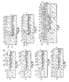
- However, semiconductor devices fabricated by said direct contact method have several serious problems which cannot be avoided in their processes. Hereinbelow, an example of a fabrication process of semiconductor devices by the direct contact method and its problems will be discussed in regard to Figures 5A to 5H. To facilitate the understanding, the figures are partly exaggerated.
- First, as shown in Figure 5A, a
field oxide film 2 for element separation is grown on a Ptype silicon substrate 1 by a well-known LOCOS (Local Oxidation of Silicon) method, and then agate oxide film 3 is formed by thermal oxidation. - Next, after a predetermined area is covered by, for example, a
photoresist 30, as shown in Figure 5B, thegate oxide film 3 in a predetermined area is etched away as shown in Figure 5C (this forms a predetermined contact part 4). - Next, as shown in Figure 5D, a polysilicon layer 5 is deposited on the entire face including the
contact part 4 by a well-known CVD (Chemical Vapor Deposition) method; and the polysilicon layer 5 is doped by, for example, phosphorus or the like to be N type; and then after a predetermined area is covered by a photoresist 40, a pattern is defined by, for example, a dry etching in order to leave only apredetermined polysilicon layer 5a (wiring layer) and 5b (gate electrode) as shown in Figure 5E. At this time, the Ptype silicon substrate 1 is also etched by patterning to form arecessed part 4a as shown in the figure. Therecessed part 4a in the figure is exaggerated to facilitate the understanding as said in the above. Also, 4b in the figure is a connecting region of thepolysilicon layer 5a and the P type silicon substrate 1 (that is, an N+ type diffusion region which will be described later). - Next, as shown in Figure 5F, the
gate oxide film 3 in a predetermined region is etched away except directly below thepolysilicon layer 5b, using theabove photoresist 40. - Next, a predetermined area is selectively ion implanted with an N type impurity (for example As) 50 and is annealed (thermal treatment) to form N+
type diffusion region 6 and 7 (source region and drain region) as shown in Figure 5G; and furthermore, an interlevel insulating layer 8 (a phosphorus glass film such as, for example, PSG (Phosphosilicate Glass) or BPSG (Borophosphosilicate Glass)) is deposited as shown in Figure 5H. - Below are the problems which are found after variously examining devices obtained by the fabrication process described in the above.
- (1) As shown Figures 5G and 5H, in addition to the above
recessed part 4a, the above connectingarea 4b in thecontact part 4 requires a predetermined region (area) in order to secure connection characteristic of the polysilicon layer (wiring layer) 5a and the N+ type diffusion region (source region) 6. Therefore, device size reduction has naturally a limit, which is disadvantageous to high degree of integration. - (2) With regard to the above Figure 5B, when the
gate oxide film 3 in the predetermined region (thecontact part 4 in Figure 5C) is removed, the other region (where agate electrode 5b will be formed later) covered with thephotoresist 30 as shown in the figure; and because thisphotoresist 30 is an organic substance, it also contaminates thegate oxide film 3 in the region which should form thegate electrode 5b (this will significantly lower the reliability of devices). Therefore, thegate oxide film 3 needs to be cleaned in the state shown in Figure 5C by using various cleaning methods, which will also be very disadvantageous in the process. - (3) Furthermore, with regard to the above Figure 5C, in the
contact part 4 with thegate oxide film 3 in the predetermined area being etched away, a natural oxide film is formed because the below lying Ptype silicon substrate 1 is exposed. In order to stabilize the connecting characteristic of the Ptype silicon substrate 1 and the polysilicon layer 5 deposited later in Figure 5D, the above natural oxide film has to be removed by a wet etching or the like with a water solution of, for example, HF (hydrogen fluoride) or the like, just before the polysilicon layer 5 is deposited (this will be, of course, disadvantageous in the process like the above (1)). However, when the nature oxide layer is etched away, thegate oxide film 3 is also etched; and the thickness of thegate oxide film 3 on which thegate electrode 5b should be formed becomes uneven, so that the reliability of the devices is significantly lowered. - (4) As described in the above, in a mask process of the
photoresist 40 or the like in Figure 5E, thecontact part 4 has to have a given excess region (area), when considering acontact part 4 wider than the contact area of thepolysilicon layer 5a, or an alignment difference, or the like. For example, if the Ptype silicon substrate 1 is exposed by the above alignment difference or the like, a dry etching or the like etches also the underlying P type silicon substrate 1 (therecessed part 4a), which significantly lowers the reliability of the devices. - From EP-A-0 272 051 a method is known which includes the steps of the precharacterizing part of
claim 1. However, no self-diffusion step is used in this method for creating or augmenting an electrical connection between a contact member and a dopant region. - A purpose of the invention is to provide semiconductor devices which are highly reliable and permit high degree of integration, and a fabrication method thereof.
- To this effect the method defined in the precharacterizing part of
claim 1 is completed by the method steps contained in the characterizing part thereof. -
- Figures 1 - 4 show embodiments of the invention;
- Figure 1 is a cross sectional view of a main part of a static RAM;
- Figure 2 is an equivalent circuit diagram of Figure 1;
- Figures 3A - 3I are cross sectional views sequentially showing the main steps of the fabrication method of the device in Figure 1; and
- Figure 4 is a cross sectional view of a device of another embodiment.
- Figures 5A - 5H are cross sectional views sequentially showing the main steps of the fabrication method of a device by a prior direct contact method.
- In reference numerals shown in the figures:
- 1...semiconductor substrate;
- 2...field oxide film;
- 3...gate oxide film;
- 5a...wiring layer;
- 5b...gate electrode;
- 6...source region (N+ type diffusion region);
- 7...drain region (N+ type diffusion region);
- 8...interlevel insulating film;
- 9...contact hole;
- 10...diffusion region;
- 11...polysilicon layer (conductive layer); and
- 12...adjacent region.
- Hereinafter, embodiments of the invention will be described.
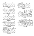
- Figures 1 - 3 show an embodiment in which the invention is applied to a static RAM.
- As shown in Figure 1, and N+
type source region 6 and an N+type drain region 7 are formed in a predetermined pattern in a major surface of a Ptype silicon substrate 1; agate electrode 5b is provided therebetween through agate oxide film 3; and an N channel MOS transistor (for example, a transistor Q4 in Figure 2) is structured. - Also, a
wiring layer 5a of a predetermined pattern (for example, thiswiring layer 5a is connected to a gate of an N channel MOS transistor Q1 in Figure 2) is formed on thegate oxide film 3 and afield oxide film 2 formed on the Ptype silicon substrate 1; an N+type diffusion region 10 is formed by self-diffusion under a contact hole 9 formed in anadjacent region 12 of thewiring layer 5a; and this N+type diffusion region 10 is connected to thesource region 6. A polysilicon layer 11 (conductive layer) is deposited into the contact hole 9, in a state of connection to the wiring layer 5a. 13 in the figure is a groove. Figure 2 is an equivalent circuit diagram showing an example of the static MOS memory. Q1 - Q6 in Figure 2 are N channel MOS transistors respectively. - As described in the above, a device of the invention includes the
wiring layer 5a of the predetermined pattern formed through thegate oxide film 3, the N+ type diffusion layer formed under the contact hole 9 formed in thegate oxide film 3 in theadjacent region 12 of thewiring layer 5a, and the polysilicon layer 11 deposited into the contact hole 9 in a state of connection to thewiring layer 5a, so that the area of a region (thegate oxide film 3 under thewiring layer 5a and theadjacent region 12 of thewiring layer 5a in Figure 1), which corresponds to the contact part 4 (the connectingregion 4b and a region of therecess part 4a) in a device by the conventional direct contact method as shown in Figure 5, can be reduced. That is, because thewiring layer 5a is connected to the polysilicon layer 11 (which is connected to the diffusion region 10) in Figure 1, the connection characteristic may be sufficiently secured in this part. Therefore, thegate oxide film 3 under thewiring layer 5a may be smaller (however, thisgate oxide film 3 may not entirely removed), so that the area of theabove wiring layer 5a and thegate oxide film 3 may be reduced. Also, because the connection to the N+ type diffusion region (source region) 6 is made by the self-diffusion of the polysilicon layer 11 buried in the contact hole 9 (that is, by the N+ type diffusion region 10), there is little need to consider an excess area by, for example, alignment difference or the like, which is very advantageous to reduction of the device size. Thus, the defects in the direct contact method may be solved, and the high degree of integration of the device is made possible, taking advantage of its characteristic. - Next, with regard to Figures 3A to 3I, a fabrication method of the device of the embodiment will be described.
- First, as shown in Figure 3A, a field oxide film 2 (for example, 8000Å thick) is grown on a P
type silicon substrate 1 by a well-known LOCOS method, and then a gate oxide film 3 (for example, 200Å thick) is formed on thesilicon substrate 1 by thermal oxidation. - Next, a polysilicon layer 5 (for example 5000Å thick) is deposited over the entire face by a well-known, for example, low pressure CVD method; then phosphorus, for example, is deposited by a CVD method at 950 degrees centigrade; and a thermal treatment is performed to dope the polysilicon layer 5 to be an N type. Furthermore, as shown in Figure 3C, after a predetermined area is covered by a mask (for example, photoresist, not shown), a predetermined pattern is defined by, for example, dry etching to form a
wiring layer 5a and agate electrode 5b. - Next, as shown in Figure 3D,
ion 60 of an N type impurity (for example As) is selectively implanted by a well-known ion implantation method, and an annealing is performed at 950 degrees centigrade to form the N+type diffusion region 6 and 7 (source region and drain region). Then, as shown in Figure 3E, an interlevel insulating layer 8 (for example, BPSG or the like) is deposited over the entire face by, for example, a normal pressure CVD method, and a steam treatment is performed at 850 degrees centigrade to planarize the interlevelinsulating layer 8 and to increase the degree of oxidation (insulation). - Next, as shown in Figure 3F, a predetermined area is covered with a mask (for example, photoresist, not shown); then a
groove 13 is formed by, for example, a dry etching of the interlevelinsulating layer 8 in a predetermined area; and a contact hole 9 is formed by etching away thepolysilicon layer 5a and removing thegate oxide film 3 by a predetermined dry etching as shown in Figure 3G. - Next, as shown in Figure 3H, a polysilicon layer 11 is deposited by a well-known decreased pressure CVD method over the entire face which includes the contact hole 9 and the
groove 13, and the polysilicon layer 11 is made low resistance by annealing at 900 degrees centigrade. At the same time, an N+type diffusion region 10 is formed by self-diffusion under the contact hole 9 to be connected to thesource region 6. This connects the polysilicon layer 11 and thewiring layer 5a. As described in the above, one process may be omitted by performing the deposition of the polysilicon layer 11 and the anneal at the same step, which is advantageous. - Next, as shown in Figure 3I, a predetermined etching is performed, and the polysilicon layer 11 is left only within the contact hole 9 and the
groove 13. - Although the latter processes are not shown, to avoid for example, a short between the polysilicon layer 11 and a metal wiring layer, a layer of SiO2 (for example, 3000Å thick) is again deposited by, for example, a well-known decreased pressure CVD method, and each normal wiring treatment is performed to complete the device.
- As is seen from the above description of the fabrication process, because the device of the embodiment and the fabrication method thereof do not require a mask process which removes the
gate oxide film 3 in the predetermined region as in the conventional direct contact method shown in Figure 5B, the reliability of the device may be secured without contamination of thegate oxide film 3. Also, because a cleaning process for the contaminatedgate oxide film 3 is not required as in conventional processes, it is an advantageous process without increased number of steps. - Also, because a process to expose the P+
type silicon substrate 1 as is shown in Figure 5C does not exist, a natural oxide film would not be formed. Therefore, adverse effects on thegate oxide film 3 by wet etching or the like (thegate oxide film 3 is also etched by this etching to have uneven film thickness) is not of concern, and the reliability of the devices can be increased. - Also, the P
type silicon substrate 1 would not be exposed by alignment difference of the mask or the like as in the patterning of the polysilicon layer 5 shown in Figure 5E (because of thegate oxide film 3 as shown in Figure 3C), the Ptype silicon substrate 1 would not be also etched by a dry etching or the like (because thegate oxide film 3 works as a mask in patterning the polysilicon layer 5). Therefore, it is advantageous for the reliability of the device. - Figure 4 shows another embodiment of the invention, for instance, an embodiment structured as a diffusion resistance element. The same reference numbers are used for the places corresponding to Figure 1.
- As shown in Figure 4, the embodiment is basically structured quite similar to the one in Figure 1, but the difference is that it is structured to have, for example, an N+
type diffusion region 10 connected to an N+ type diffusion region 6 (the source region in the embodiment in Figure 1) in the region where thegate electrode 5b and thedrain region 7 are formed in Figure 1 (the region in the right side of Figure 1). That is, the gate electrode as in the above embodiment of Figure 1 does not exist; the above structure is provided symmetrically with the N+type diffusion region 6 in-between; the twodiffusion regions 10 are each connected to the N+type diffusion region 6; and the diffusion resistance is formed there. - 21 in the figure are electrodes to take out the
wiring layer 5a; 22 are through holes; and 23 is a SiO2 layer. - Since the device of the embodiment has the similar structure as in the above embodiment of Figure 1, it has the same advantage as in the above embodiment, and it is also structurally convenient for electrical testing.
- That is, a direct contact structure of the invention may be easily checked by using the two
diffusion regions 10 and thediffusion region 6 connected thereto shown in the figure as a diffusion resistance and measuring the electric characteristics thereof. - Resistive valve of 30 - 50 ohm per 1 contact hole may be actually freely controlled, and also very good contact characteristic may be obtained.
- Next, a fabrication method of the device of the embodiment is briefly described regarding Figure 3; in processing from the state in Figure 3B to the state in Figure 3C, instead of forming the
gate electrode 5b, thewiring layer 5a of the predetermined pattern is formed also in the opposing region (in Figure 3, thefield oxide film 2 or the like in the opposing region is omitted). Then as in Figure 3D, the N+ type diffusion region 6 (7) is selectively formed in a predetermined region by an ion implantation and a thermal treatment; in Figure 3E and on, an insulatinglayer 23 is formed after each similar process; and then each wiring treatment completes the device in Figure 4. - Although the invention has been illustrated hereinabove, the above embodiments may be modified based on the technical idea of the invention.
- For example, although polysilicon is used for the conductive layer 11 deposited into the contact hole 9 in the above embodiments, other metal such as Al or the like may be deposited (in this case, metal or the like is deposited after the
diffusion layer 10 is previously formed by an impurity diffusion by a conventional art). Also in the above embodiments, the deposition of the conductive layer (polysilicon layer) 11 and the formation of thediffusion layer 10 by annealing may be performed at the same time. Or, the conductive layer 11 may be deposited after the formation of thediffusion layer 10. Or, the diffusion may be performed by an adequate optical excitation treatment such as laser anneal, lamp anneal, or the like. - Although the invention is applied to, for example, the N channel MOS transistor Q4 and Q1 within broken lines in Figure 2 in the above embodiments (that is, it is used for connecting the source of the transistor Q4 and the gate of the transistor Q1), it may also be applied for connecting the drain of the transistor Q5 and the gate of the transistor Q2, and connecting the source of the transistor Q4 and the drain of the transistor Q2, and so on, in the same figure.
- Also, the invention may be applied to appropriate places in other devices.
- The conductivity types of the each above semiconductor region may be reversed, and the invention may be applied to the appropriate other than static RAMs, for example dynamic RAMs or the like.
- As described above, because the invention comprises: a wiring layer with a predetermined pattern formed over a major surface of a semiconductor substrate through an insulating film, a diffusion layer formed under a contact hole formed in said insulation film in an adjacent region of the wiring layer, and a conductive layer deposited into said contact hole in a state of being connected to said wiring layer, are occupied by said insulating film and wiring layer and also area of the adjacent region of said wiring layer may be reduced, which allows high degree of integration.
- Also, because the contact hole is formed after patterning of the wiring layer over said insulating film, a process of etching said insulating film may be performed without contamination or the like of said insulating film.
- Also, because a semiconductor substrate is protected by said insulating film, no exposure or the like of the semiconductor substrate occurs, nor does etching or the like of said semiconductor substrate in patterning or the like of said wiring film. Therefore, highly reliable semiconductor devices and the fabrication method thereof may be provided.
Claims (7)
- A method of making a semiconductor device comprising: providing a semiconductor substrate (1) of one conductivity type and having a top surface,forming at least one doped region (6) having a dopant impurity of the other conductivity type in the semiconductor substrate of one conductivity type and opening onto the top surface thereof,forming an insulation layer (3) on the top surface of the semiconductor substrate of one conductivity type, to include a relatively thick insulation region (2) and an adjoining relatively thin insulation region (3),forming a wiring layer (5a) of electrically conductive material over the insulation layer,patterning the wiring layer of electrically conductive material, to expose a portion of the relatively thin insulation region (3) of the insulation layer therebeneath,forming an interlevel insulating layer (8) over the patterned wiring layer (5a) and the previously-formed insulation layer (3),forming a contact hole (9) through said interlevel insulating layer (8), said patterned wiring layer (5a), and said insulation layer (3) andforming an electrically conductive contact member (11) of material having a dopant impurity of said other conductivity type in the contact hole in engagement with said patterned wiring layer such that the electrically conductive contact member (11) fills the contact hole and extends through said interlevel insulating layer (8) and the relatively thin insulation region of said insulation layer into engagement with the top surface of said semiconductor substrate of one conductivity type and said one doped region of the other conductivity type,characterized in thatthe formation of at least one doped region (6) of the other conductivity type in the semiconductor substrate of one conductivity type occurs after the formation of the insulation layer on the top surface of the semiconductor substrate of said one conductivity type and the formation and patterning of the layer of electrically conductive material over the insulation layer, and is accomplished through the portion of the relatively thin insulation region of the insulation layer exposed by the patterning of the layer of electrically conductive material in defining the wiring layer of electrically conductive material, so that the patterned wiring layer of electrically conductive material is aligned with respect to said at least one doped region having a dopant impurity of said other conductivity type,the contact hole is formed by removing a portion of said patterned wiring layer (5a) and a corresponding portion of the relatively thin insulation region (3) of said insulation layer therebeneath to expose the top surface of the semiconductor substrate of one conductivity type and of said one doped region located in a position partially exposing said one doped region of the other conductivity type which opens onto the top surface of the semiconductor substrate of one conductivity type while also exposing a portion of the top surface of the semiconductor substrate of one conductivity type anddopant impurity of the other conductivity type is diffused from said electrically conductive contact member as formed in the contact hole into said semiconductor substrate of one conductivity type to define a diffused doped region (10) of the other conductivity type spanning the contact hole and extending across said semiconductor substrate of said one conductivity type to merge with said one doped region of the other conductivity type to at least augment the electrical connection between the contact member and said one doped region of the other conductivity type.
- A method of making a semiconductor device as set forth in Claim 1, further characterized in that the formation of said at least one doped region (6) of the other conductivity type is accomplished by selective ion implantation of the dopant impurity of the other conductivity type into the semiconductor substrate of said one conductivity type.
- A method of making a semiconductor device as set forth in either of Claims 1-2, further characterized in that the wiring layer is formed over the insulation layer by depositing a layer of polycrystalline semiconductor material over the insulation layer,providing the layer of polycrystalline semiconductor material with a dopant impurity of the other conductivity type, anddefining the wiring layer of electrically conductive material by patterning the layer of polycrystalline semiconductor material.
- A method of making a semiconductor device as set forth in Claim 3, further characterized in that the contact member is formed in the contact hole by depositing a second layer of polycrystalline semiconductor material over the insulation layer and filling the contact hole extending therethrough,providing the second layer of polycrystalline semiconductor material with a dopant impurity of the other conductivity type, anddefining the contact member of electrically conductive material by removing all of the second layer of polycrystalline semiconductor material except for the portion thereof within the contact hole.
- A method of making a semiconductor device as set forth in Claim 4, further characterized bysubjecting the second layer of polycrystalline semiconductor material to heat annealing to lower the electrical resistance thereof sufficiently to make the material electrically conductive, andthereafter defining the contact member of electrically conductive material by removing all of the annealed second layer of polycrystalline semiconductor material except for the portion thereof within the contact hole.
- A method of making a semiconductor device as set forth in Claim 5, further characterized in that the diffusion of the dopant impurity of the other conductivity type from the electrically conductive contact member into said semiconductor substrate of one conductivity type occurs in response to the heat annealing of the second layer of polycrystalline semiconductor material.
- A method of making a semiconductor device as set forth in any of Claims 1-6, further characterized in thatin the step of patterning the wiring layer of electrically conductive material, a gate electrode (5b), disposed on the relatively thin insulation region (3) of the insulation layer and positioned over a portion of the semiconductor substrate (1) of said one conductivity type, is formed,in said step of forming at least one doped region, a pair of spaced apart doped regions (6,7) having a dopant impurity of the other conductivity type are formed in the semiconductor substrate of said one conductivity type, open onto the top surface thereof and aligned with said gate electrode,said pair of doped regions of the other conductivity type being respectively a source region and a drain region,said electrically conductive contact member of material having a dopant impurity of said other conductivity type is formed in the contact hole in engagement with said patterned wiring layer and one of the source and drain regions of the other conductivity type spaced from said gate electrode, andsaid dopant impurity of the other conductivity type is diffused from said electrically conductive contact member into said semiconductor substrate of one conductivity type, thereby defining the diffused doped region of the other conductivity type spanning the contact hole and extending across said semiconductor substrate of said one conductivity type to merge with said one of the source and drain regions of the other conductivity type to at least augment the electrical connection between the contact member and said one of said source and drain regions of the other conductivity type.
Applications Claiming Priority (2)
| Application Number | Priority Date | Filing Date | Title |
|---|---|---|---|
| JP21807/89 | 1989-01-31 | ||
| JP1021807A JPH02202054A (en) | 1989-01-31 | 1989-01-31 | Semiconductor device and its manufacture |
Publications (3)
| Publication Number | Publication Date |
|---|---|
| EP0380964A2 EP0380964A2 (en) | 1990-08-08 |
| EP0380964A3 EP0380964A3 (en) | 1991-03-13 |
| EP0380964B1 true EP0380964B1 (en) | 1997-05-21 |
Family
ID=12065325
Family Applications (1)
| Application Number | Title | Priority Date | Filing Date |
|---|---|---|---|
| EP90100909A Expired - Lifetime EP0380964B1 (en) | 1989-01-31 | 1990-01-17 | Method of making a semiconductor device having a contact member |
Country Status (3)
| Country | Link |
|---|---|
| EP (1) | EP0380964B1 (en) |
| JP (1) | JPH02202054A (en) |
| DE (1) | DE69030743T2 (en) |
Families Citing this family (2)
| Publication number | Priority date | Publication date | Assignee | Title |
|---|---|---|---|---|
| GB9219268D0 (en) * | 1992-09-11 | 1992-10-28 | Inmos Ltd | Semiconductor device incorporating a contact and manufacture thereof |
| JP3256048B2 (en) * | 1993-09-20 | 2002-02-12 | 富士通株式会社 | Semiconductor device and manufacturing method thereof |
Family Cites Families (2)
| Publication number | Priority date | Publication date | Assignee | Title |
|---|---|---|---|---|
| JPS59220952A (en) * | 1983-05-31 | 1984-12-12 | Toshiba Corp | Manufacture of semiconductor device |
| ATE80750T1 (en) * | 1986-12-17 | 1992-10-15 | Advanced Micro Devices Inc | JOINTED CONTACT STRUCTURE WITH REDUCED AREA REQUIREMENTS. |
-
1989
- 1989-01-31 JP JP1021807A patent/JPH02202054A/en active Pending
-
1990
- 1990-01-17 DE DE1990630743 patent/DE69030743T2/en not_active Expired - Fee Related
- 1990-01-17 EP EP90100909A patent/EP0380964B1/en not_active Expired - Lifetime
Non-Patent Citations (1)
| Title |
|---|
| "VLSI Technology", S.M.Sze, 1983, pages 169-171 * |
Also Published As
| Publication number | Publication date |
|---|---|
| JPH02202054A (en) | 1990-08-10 |
| DE69030743D1 (en) | 1997-06-26 |
| EP0380964A2 (en) | 1990-08-08 |
| EP0380964A3 (en) | 1991-03-13 |
| DE69030743T2 (en) | 1997-11-13 |
Similar Documents
| Publication | Publication Date | Title |
|---|---|---|
| US5385857A (en) | Method of manufacturing a semiconductor device with high packing density and having field effect transistors | |
| US4466172A (en) | Method for fabricating MOS device with self-aligned contacts | |
| KR0144906B1 (en) | Nonvolatile Memory Device and Manufacturing Method Thereof | |
| US5061651A (en) | Method of making dram cell with stacked capacitor | |
| US4984055A (en) | Semiconductor device having a plurality of conductive layers and manufacturing method therefor | |
| US4849854A (en) | Semiconductor device and method of manufacturing the same | |
| US4446613A (en) | Integrated circuit resistor and method of fabrication | |
| US5091768A (en) | Semiconductor device having a funnel shaped inter-level connection | |
| US5627095A (en) | Method for fabricating semiconductor devices having bit lines and storage node contacts | |
| US5043298A (en) | Process for manufacturing a DRAM cell | |
| US6426528B2 (en) | Method of fabricating conductive straps to interconnect contacts to corresponding digit lines by employing an angled sidewall implant and semiconductor devices fabricated thereby | |
| EP0535694A2 (en) | Semiconductor memory device and method of manufacturing the same | |
| KR930009016B1 (en) | Wiring contact structure of semiconductor device and manufacturing method | |
| JP3897934B2 (en) | Contact hole manufacturing method of semiconductor device | |
| US6040221A (en) | Semiconductor processing methods of forming a buried contact, a conductive line, an electrical connection to a buried contact area, and a field effect transistor gate | |
| US4616402A (en) | Method of manufacturing a semiconductor device with a stacked-gate-electrode structure | |
| US7332811B2 (en) | Integrated circuit interconnect | |
| EP0160965B1 (en) | Method of manufacturing a semiconductor device with a stacked-gate-electrode structure | |
| US5243219A (en) | Semiconductor device having impurity diffusion region formed in substrate beneath interlayer contact hole | |
| US6825112B2 (en) | Semiconductor device and method of production thereof | |
| EP0380964B1 (en) | Method of making a semiconductor device having a contact member | |
| US5221634A (en) | Method of making semiconductor device employing self diffusion of dopant from contact member for augmenting electrical connection to doped region in substrate | |
| JPH10335450A (en) | Semiconductor device and its manufacture | |
| JPH1197529A (en) | Manufacture of semiconductor device | |
| KR100200697B1 (en) | Semiconductor device with guard ring and method of forming contact using guarding ring |
Legal Events
| Date | Code | Title | Description |
|---|---|---|---|
| PUAI | Public reference made under article 153(3) epc to a published international application that has entered the european phase |
Free format text: ORIGINAL CODE: 0009012 |
|
| AK | Designated contracting states |
Kind code of ref document: A2 Designated state(s): DE FR GB IT NL |
|
| PUAL | Search report despatched |
Free format text: ORIGINAL CODE: 0009013 |
|
| AK | Designated contracting states |
Kind code of ref document: A3 Designated state(s): DE FR GB IT NL |
|
| 17P | Request for examination filed |
Effective date: 19910910 |
|
| 17Q | First examination report despatched |
Effective date: 19940210 |
|
| GRAG | Despatch of communication of intention to grant |
Free format text: ORIGINAL CODE: EPIDOS AGRA |
|
| GRAH | Despatch of communication of intention to grant a patent |
Free format text: ORIGINAL CODE: EPIDOS IGRA |
|
| GRAH | Despatch of communication of intention to grant a patent |
Free format text: ORIGINAL CODE: EPIDOS IGRA |
|
| GRAA | (expected) grant |
Free format text: ORIGINAL CODE: 0009210 |
|
| ITF | It: translation for a ep patent filed |
Owner name: BARZANO' E ZANARDO ROMA S.P.A. |
|
| AK | Designated contracting states |
Kind code of ref document: B1 Designated state(s): DE FR GB IT NL |
|
| PG25 | Lapsed in a contracting state [announced via postgrant information from national office to epo] |
Ref country code: NL Free format text: LAPSE BECAUSE OF FAILURE TO SUBMIT A TRANSLATION OF THE DESCRIPTION OR TO PAY THE FEE WITHIN THE PRESCRIBED TIME-LIMIT Effective date: 19970521 |
|
| REF | Corresponds to: |
Ref document number: 69030743 Country of ref document: DE Date of ref document: 19970626 |
|
| ET | Fr: translation filed | ||
| NLV1 | Nl: lapsed or annulled due to failure to fulfill the requirements of art. 29p and 29m of the patents act | ||
| PLBE | No opposition filed within time limit |
Free format text: ORIGINAL CODE: 0009261 |
|
| STAA | Information on the status of an ep patent application or granted ep patent |
Free format text: STATUS: NO OPPOSITION FILED WITHIN TIME LIMIT |
|
| 26N | No opposition filed | ||
| REG | Reference to a national code |
Ref country code: GB Ref legal event code: IF02 |
|
| PGFP | Annual fee paid to national office [announced via postgrant information from national office to epo] |
Ref country code: GB Payment date: 20061213 Year of fee payment: 18 |
|
| PGFP | Annual fee paid to national office [announced via postgrant information from national office to epo] |
Ref country code: DE Payment date: 20070131 Year of fee payment: 18 |
|
| PGFP | Annual fee paid to national office [announced via postgrant information from national office to epo] |
Ref country code: IT Payment date: 20070627 Year of fee payment: 18 |
|
| PGFP | Annual fee paid to national office [announced via postgrant information from national office to epo] |
Ref country code: FR Payment date: 20070103 Year of fee payment: 18 |
|
| GBPC | Gb: european patent ceased through non-payment of renewal fee |
Effective date: 20080117 |
|
| PG25 | Lapsed in a contracting state [announced via postgrant information from national office to epo] |
Ref country code: DE Free format text: LAPSE BECAUSE OF NON-PAYMENT OF DUE FEES Effective date: 20080801 |
|
| REG | Reference to a national code |
Ref country code: FR Ref legal event code: ST Effective date: 20081029 |
|
| PG25 | Lapsed in a contracting state [announced via postgrant information from national office to epo] |
Ref country code: GB Free format text: LAPSE BECAUSE OF NON-PAYMENT OF DUE FEES Effective date: 20080117 |
|
| PG25 | Lapsed in a contracting state [announced via postgrant information from national office to epo] |
Ref country code: FR Free format text: LAPSE BECAUSE OF NON-PAYMENT OF DUE FEES Effective date: 20080131 |
|
| PG25 | Lapsed in a contracting state [announced via postgrant information from national office to epo] |
Ref country code: IT Free format text: LAPSE BECAUSE OF NON-PAYMENT OF DUE FEES Effective date: 20080117 |