EP0380521B1 - PARALLEL PIPELINE IMAGE PROCESSOR WITH 2x2 WINDOW ARCHITECTURE - Google Patents
PARALLEL PIPELINE IMAGE PROCESSOR WITH 2x2 WINDOW ARCHITECTURE Download PDFInfo
- Publication number
- EP0380521B1 EP0380521B1 EP88908014A EP88908014A EP0380521B1 EP 0380521 B1 EP0380521 B1 EP 0380521B1 EP 88908014 A EP88908014 A EP 88908014A EP 88908014 A EP88908014 A EP 88908014A EP 0380521 B1 EP0380521 B1 EP 0380521B1
- Authority
- EP
- European Patent Office
- Prior art keywords
- output
- data
- storage
- input
- register
- Prior art date
- Legal status (The legal status is an assumption and is not a legal conclusion. Google has not performed a legal analysis and makes no representation as to the accuracy of the status listed.)
- Expired - Lifetime
Links
Images


Classifications
-
- G—PHYSICS
- G06—COMPUTING; CALCULATING OR COUNTING
- G06T—IMAGE DATA PROCESSING OR GENERATION, IN GENERAL
- G06T1/00—General purpose image data processing
-
- G—PHYSICS
- G06—COMPUTING; CALCULATING OR COUNTING
- G06T—IMAGE DATA PROCESSING OR GENERATION, IN GENERAL
- G06T5/00—Image enhancement or restoration
- G06T5/20—Image enhancement or restoration by the use of local operators
Abstract
Description
- This invention relates to image processors. In particular, a 2 x 2 window serial neighborhood transformation processor operates on separate segments of a partitioned image data matrix.
- Neighborhood image processors are a class of devices that operate upon a first array or matrix of image sensor data values stored in cells or registers of an image data memory. The image data values stored in each of the cells generally originate from discrete pixels in the image generated by a 2-dimensional sensor plane responsive to light projected thereon. Neighborhood image processors operate on the image data values to generate subsequent transformation matrixes in which each cell thereof has a value depending upon its value in the preceding matrix of the image data memory and the values of its surrounding or neighboring cells in the preceding matrix. In turn, subsequent transformations can be generated by operating on the previous transformation matrix. Neighborhood transformation processes are crucial to efficient low-level, high-data rate processing in image processing, image understanding, machine vision applications, and the like. Computational requirements of neighborhood transformation processors can be in the billions of operations per second. This is so because of the high data rates involved in image processing (about 8 million pixels per second for 525 line T.V. video) and large number of operations which must be performed in executing algorithms (several hundred operations per pixel). Neighborhood transformation processors have proven to be effective in extracting many primitive characteristics from imagery which are valuable in understanding image content and in image data compression (for example, finding boundaries or edges of objects, i.e. Sobel and Roberts edges).
- The present invention is intended to be applicable to any two dimensional array of image data which needs to be transformed by the neighborhood transformation process.
- An example of a neighborhood image processor is disclosed in U.S. Patent 4,484,349, issued to David L. McCubbrey, and is herein incorporated by reference. McCubbrey discloses a serial neighborhood processor which employs a chain or a pipeline of individually programmable serial neighborhood transformation stages. Each stage is capable of generating the transformed value of one pixel within a single clock pulse interval. The output of each serial neighborhood transformation stage occurs at the same rate as its input. This allows the output of one stage to be provided to the input of a subsequent stage which may perform different neighborhood transformations. Each stage thus performs one specific transformation over the entire image.
- Further, McCubbrey discloses the technique of partitioning the image matrix so that contiguous segments of the image can be processed simultaneously by two or more adjacent serial neighborhood transformation processors. In such a system, provisions must be provided to bi-directionally transfer data between adjacent serial neighborhood processors. This transfer becomes necessary when neighboring cells of the cell being transformed in one processor is contained in the image matrix segment of an adjacent image matrix segment.
- In US-A 4 484 349 the image memory matrix is scanned by means of 3X3 pixel window. Another image analyzer for pattern recognition is known from US-A 4 395 699 which employs at least one neighborhood transformation stage for analyzing groups of neighborhood pixel values and selectively transforming the pixel values as a result of the analysis. The center pixel in the 3X3 window is changed to a programmable transformation value if it and its neighboring pixels have particular values. A programmable memory loaded by a central controller is utilized to determine whether neighboring pixels of particular values are configured in a preselected pattern.
- Patent Abstracts of Japan, Vol. 9, No. 285 (P-404) in the abstract of JP 60-124785 describes a picture processing unit using a 2X2 bit window together with registers storing the difference between an address of the specific bit in the window and an address of other bits. Adder circuits add specific bits at write/read operation of the memory unit. These are accessed by using the address of the specific bit and the address of the adder circuit. All bits in the window of the picture memory are read by one accessing.
- The object of the present invention is to provide a simple architecture for a neighborhood transformation module which can be incorporated into a parallel pipeline image processor.
- Another object of the invention is to provide a neighborhood transformation module architecture which performs neighborhood transformations on a 2 x 2 window.
- The present invention as claimed contemplates a neighborhood transformation module (NTM) for performing a 2 x 2 window transformation. In the present invention, the NTM is comprised of two storage registers separated by a segment delay. The input to the first storage register, the outputs of the first and second storage registers and the output of the segment delay are presented to a multipath switch for subsequent neighborhood transformation processing. Further, the 2 x 2 neighborhood transformation module architecture also includes two shift registers and an additional storage register for transferring data between parallel neighborhood transformation modules.
- In the preferred embodiment, one of the shift registers of the NTM module latches onto an edge data value for availability by adjacent (parallel) NTM modules. The binary data of the shift register is serially passed to an adjacent NTM's input shift register. The input shift register is appropriately connected to the multipath switch so that the neighborhood transformation can be performed using adjacent NTM's edge data.
- Further, the present invention contemplates the use of raster scan reversals in combination with the 2 x 2 window neighborhood transformation scheme. The neighborhood transformation module architecture of the present invention permits the scan reversal by the same NTM architecture without any additional change in hardware or control synchronization.
- Figure 1 is a block diagram of a parallel partition serial neighborhood image processing system.
- Figure 2 is a block diagram of a neighborhood transformation module in accordance with the present invention.
- Figure 3 is a block diagram showing the interconnection of three parallel neighborhood transformation modules.
- Figures 4a - 4d are diagramatic representations of raster scan control schemes.
- Figure 5 is a diagram illustrating the neighborhood transformation windows on a memory map.
- Figure 6 is a clock cycle timing illustrating the operation of the neighborhood transformation module of Figure 2.
- Figure 7 is a memory map of a 3-segment partitioned memory in accordance with the present invention.
- Figure 8 is a clock cycle timing table illustrating the operation of the neighborhood transformation module with the reverse scan of Figure 4b.
- Figure 9 is another embodiment of the neighborhood transformation module in accordance with the present invention.
- Illustrated in Figure 1 is a parallel pipeline image processor similar to that shown in U.S. Patent 4,484,349 described earlier. Image sensor data from a two dimensional
image sensor plane 10 having N-columns and M-rows is transferred to an image data memory means 20. For exposition purposes, thememory 20 can be visualized as a two dimensional array of storage registers also having M-rows and N-columns. Each of the registers inmemory 20 can be addressed by its row and column address. As should be understood by those skilled in the art, many techniques of memory rapping may be employed to obtain the intended result of keeping track of the location of the image. Further illustrated in Figure 1,memory 20 is geographically divided into K-partitions (K = 3 in the drawing) numerically identified as 21, 22, and 23. Each of the partitions is comprised of M-rows and P-columns. In the present invention, the partitions are preferably identical in array size. - Data from a
first partition 21 is serially presented to neighborhood transformation module (NTM) 30. The output ofNTM 30 is serially presented to NTM 40. Theoutput 60 ofNTM 40 is shown coupled back into memory means 20. - In a similar manner, a
second partition 22 of memory means 20 is serially presented toNTM 31 andNTM 41 in succession. The output 61 ofNTM 41 is coupled back to memory means 20. Likewise, the 3rd partition identified by the numeral 23 is presented toNTM 32 andNTM 42 in succession, and theoutput 62 ofmodule 42 is also coupled back to memory means 20. - In practice,
NTM modules NTM modules NTM modules NTM modules - Again referring to Figure 1, interconnection means 51 provides a path for transferring edge data between
modules modules modules modules - It should be recognized by those skilled in the art that there may be a number of partitions between the second partition identified by
numeral 22 and the 3rd partition identified bynumeral 23. The number of partitions selected is a matter of design choice. - Also shown in Figure 1,
memory 20 includes an output means 70 which is generally intended to be connected to autilization device 71, such as display electronics for video output. However, it should also be recognized that the output ofmodules - The description so far presented is, in part, essentially that known in the art, and particularly described by U.S. Patent 4,484,349. Illustrated in Figure 2 is a schematic block diagram of one of the neighborhood transformation modules shown in Figure 1 in accordance with the present invention in which a 2 x 2 window transformation is an integral part of the transformation process. In Figure 2, the single signal lines illustrated may actually be a plurality of signal lines, i.e. a parallel signal bus.
- The architecture of the
neighborhood transformation module 100 illustrated in Figure 2 is operative to perform a 2 x 2 window neighborhood transformation as aforesaid, and may be used for any of the NTM modules of Figure 1. Each NTM module includes an input means 201 presented to a storage register (SR) 203.Storage register 203 includes anoutput 204, also identified by the signal letter "A", which is presented to an input ofstorage register 205 andmultipath switch 207 on connection means 204a and 204b, respectively.Storage register 205 includes anoutput 206, also identified by the signal letter "B", presented tooutput shift register 211,delay register 212, andmultipath switch 207 on connection means 206a, 206b, and 206c, respectively.Output shift register 211 includes anoutput 218 also identified by signal letter "H". Delayregister 212 includes anoutput 213, also identified by the signal letter "C", presented tostorage register 215 andmultipath switch 207 on connection means 213a and 213b, respectively.Storage register 215 includes anoutput 219, also identified by the signal letter "D", presented tomultipath switch 207. -
Module 100 further includesinput shift register 221 having itsoutput 225, also identified by signal letter F, presented tostorage register 223 andmultipath switch 207 on connection means 225a and 225b, respectively. Theoutput 227, also identified by signal letter G, ofstorage register 223 is connected tomultipath switch 207 on connection means 227. Theinput shift register 221 receives its input via input means 231 or 233 throughmultiplexer 235 under control of switch control S2. -
Multipath switch 207 provides fouroutputs neighborhood transformation processor 250 which includes arithmetic logic units (ALU) 251, 252 and 253.ALU 251 operates on signals "a" and "b", andALU 252 operates on signals "c" and "d". The output ofALU 251 is presented toALU 253 through astorage register 255. Similarly the output ofALU 252 is presented toALU 253 throughstorage register 257. It should be noted that the input, output, and internal connections ofprocessor 250 as just described is only exemplary in nature for performing the intended function. - Each of the storage registers, the
delay register 212, and arithmetic logic units are intended to be synchronously operated by a central clock signal CK1 (not shown). The clock signal CK1 has been left out of the diagram in order to simplify the drawing for ease in understanding the present invention. (synchronous and asynchronous control being well understood in the control arts). Both theoutput shift register 211 and theinput shift register 221 are shown to be serially shifted by a common clock signal CK2. However, independent clock signals may be utilized. (It should be noted that the input to shiftregister 221 and the output ofshift register 211 are serial in form, and therefore simplifies the architecture since no parallel bus line is required). Further,output shift register 211 also includes an enabling signal E1 to cause the storage of the output ofregister 205, under control of E1.Storage register 223 also includes enabling signal E2 to cause the storage of the output ofinput shift register 221 under control of E2. Lastly,multipath switch 207 is illustrated having a control switch signal S1 which will function in a manner as will be described below. - Figure 3 illustrates the parallel pipeline neighborhood transformation processor of the present invention in which the array is divided into three partitions. The purpose of Figure 3 is to illustrate the connections between three identical
neighborhood transformation modules 100, and in particular show the connections between the output andinput shift register - In Figure 3, the left hand NTM module is identified as
module 301, the right hand NTM module is identified as 303, and the middle NTM module is identified as 302. All of theNTM modules modules NTM modules NTM module 100 of Figure 2. The output ofoutput shift register 211 ofmodule 302 is connected to input means 233 of precedingmodule 301 and input means 231 of followingmodule 303. The output ofshift register 211 ofmodule 301 is presented to input means 231 of followingmodule 302. The output ofoutput shift register 211 ofmodule 303 is presented to input means 233 of precedingmodule 302. - Figures 4a, 4b, 4c, and 4d illustrate raster line scan control schemes and a neighborhood transformation memory mapping scheme in accordance with the present invention. In particular, Figure 4a shows a raster line scan moving from left to right and from top to bottom - i.e., right/down-scan. Further, data of the 2 x 2 window having four corner addresses a, b, c, and d are operated on with the decision that the resultant transformation of the aforesaid 4 corner data values will be stored in the memory means 20 address location corresponding to the former location of the b-address. The above control scheme is further illustrated in Figure 5.
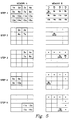
- Figure 5 illustrates a small matrix example of addresses in memory A having 4 columns and 4 rows. Each of the cells in the memory A matrix is identified by a numeric address 1a to 16a. At
Step 1, a first 2 x 2 neighborhood transformation operates on data incells address 5b of memory B - memory B having corresponding numeral addresses as memory A. InStep 2 the raster scan moves over 1 column and performs the neighborhood transformation on data incells cell 6b. AfterStep 3, the result of the neighborhood transformation oncells address 7b and identified as NT3. Note that afterStep 3, no further valid 2 x 2 window transformations can be performed on data values inrows cell 8b. At the end ofStep 4, the raster line scan is reset down one row and back to the left side as illustrated by Step K. In Step K, a neighborhood transformation NT4 is performed oncells address 9b. Step N illustrates the next to the last 2 x 2 window transformation to be performed on data values in the matrix off data values stored in memory A. In Step N, a neighborhood transformation NT11 is performed oncells address 15b. - It should be recognized by those skilled in the art, that after a complete raster scan of an image stored in memory A, and utilization of a 2 x 2 window neighborhood transformation scan, and utilization of the storage of the resultant transformations in corresponding addresses of the b cell in memory B, the resulting image is one in which the image shrinks because the top row and the right column no longer have valid neighborhood transformation data. This is particularly indicated in Figure 5 by the asterisks in the top row and right column of memory B after Step N. Further, the resultant image in the memory matrix has shifted down one row and to the left one column.
- It should be appreciated by those skilled in the art that for each neighborhood transformation, for example by the second transformation by
NTM modules - The operation of the neighborhood transformation module of Figure 2 will be described with reference to Figure 3, the clock cycle timing table presented in Figure 6, the memory diagrams of Figure 7, and the raster line scan diagram of Figure 4a.
- Figure 7 illustrates 3-segment partitioned image data memory maps A, B and A+ similar to Figure 5. Each memory map has 4 rows and 12 columns. Further, consider that the image data and corresponding memory map is divided into 3 segments as illustrated in
memory map segments address 1, and the lowest right hand cell identified byaddress 16. Further, it should be assumed that the output data from thememory partitions transformation modules 301 302,and 303, respectively, as illustrated in Figure 3 in accordance with the raster line scan as illustrated in Figure 4a. That is, the cell data is sequentially fed, for a selected clock cycle, from the memory, one cell at a time and one line at a time, starting with the address corresponding to the upper left corner of the memory map and scanning from the left to the right for each line scan. The details in Figure 6 show the address of the data (not the data itself) on input means a, b, c and d which are presented to theneighborhood transformation processor 250 for each clock cycle CK1. - The clock cycle timing table in Figure 6 and the memory map diagrams illustrated in Figure 7 diagrammatically illustrate the operation of any of the NTM modules, but particularly for the
middle NTM module 302, for a right/down-scan. The heading of the table of Figure 6 indicates the signal letters as defined earlier with respect to Figure 2. The numeral under the "letter" columns indicate the cell address of the particular partitioned memory. The following exposition describes the flow of data following each complete clock cycle CK1. The "circled" cells indicate needed edge data by the adjacent NTM module. "Boxed" cell data indicates the cell data required for the neighborhood 2 x 2 transformation. - After the the second clock cycle, signal B, containing data of
cell 1, is loaded intoshift register 211 upon command of signal E1. In the timing background for the example illustrated, at a generally faster clock rate CK2, the contents ofoutput shift register 211 is serially shifted into theinput shift register 221 of the precedingNTM module 301 through connectingmeans 231. At the same time the contents of theoutput shift register 211 of the followingNTM module 303 is serially shifted intoinput shift register 221 ofmodule 302 through connectingmeans 233. Upon command of signal E2, signal F is loaded intoSR 223. In like manner, after the 6th clock cycle, the contents ofcell 5 is loaded intoinput shift register 221. Thus, before the 10th clock cycle, signal G represents the contents ofcell 1 and signal F represents the contents ofcell 5. The combination ofoutput shift register 211 andinput shift register 221 allows passage and storage of edge data over a single serial data transmission line between NTM modules. This allows, therefore, background timing activity while cell data is passed throughregisters - Generally, it should be noted that clock rate CK2 need not be faster than CK1, and may actually be the same as CK1. That is, CK2 may be the same as CK1 (or even slower) if the number of columns per segment is greater than the number of bits per data value stored in a memory cell (i.e., the length of the output serial shift register, eg. register 211).
- A discussion of the function of the
delay register 212 and the size of delay will now be presented. In the example as illustrated in Figure 6, the memory image is divided into 3 segments in which each segment includes 4 columns. For proper operation of theNTM module 100, delay register 212 must be equivalent to N-total-image-columns (12) divided by the number of K-partitions (3) less 1 - i.e., (N/K) -1. In the instant example, the delay register must provide the equivalent of 3 clock cycles (12 divided by 3 less 1). Therefore, in the present example, the delay register must be the equivalent of 3 clock cycles long before data is available at thedelay register output 213, identified by the letter "C". Accordingly, the contents of cell no. 1 is available at C after the fifth clock cycle. After the sixth clock cycle, the value of signals A, B, C, and D are precisely the window pattern of Figure 4a and the window illustrated atStep 1 of Figure 5 for memory A. Namely, D has the value of cell no. 1, and C has the value of cell no. 2, B has the cell value of no. 5, and A has the value of cell no. 6. In like manner, after each clock cycle CK1, the values of A, B, C, and D correspond to the scanning 2 x 2 window. - The discussion which follows describes the operation of the multipath switch in order to perform neighborhood transformations at partition edges. After the sixth clock cycle
multipath switch 207 is set by switch S1 to present the outputs A, B, C and D as the inputs a, b, c and d toneighborhood transformation processor 250. After the 7th clock cycle, the beginning of the neighborhood transformation ofcells processor 250. The transformation process takes place sequentially through one or more clock cycles until the data is available at theoutput 290 ofprocessor 250 for subsequent storage in memory B or presentation to a subsequent transformation stage as illustrated in Figure 1. Assuming there is only one transformation stage, the data represented by signals A, B, C, and D after the 6th, 7th, and 8th clock cycles correspond to the 2 x 2 window moving as shown bySteps multipath switch 207 control signal S1 is such to allow signals A, B, C, and D to become the input signals a, b, c, and d presented to theneighborhood processor 250. Therefore, the neighborhood transformation values NT1, NT2, and NT3 can be calculated sequentially by the neighborhood transformation processor. - However, after the 9th clock cycle, the middle NTM module requires edge data from the following
NTM module 303. In these circumstances, switch control S1 is changed to control themultipath switch 207 to cause the connection of signal G toprocessor 250 input signal a, and signal F toprocessor 250 input signal c. At this point,processor 250 can perform the neighborhood transformation NT4 on the proper 2 x 2 window cell data as illustrated bywindow 610 in Figure 7. - After the 9th clock cycle,
SR 223 is again enabled to store signal F. Further, after the 10th clock cycle,cell 9 is serially passed to input register 221 for use after the 13th clock cycle when edge data is again required to obtain the NT8 transformation. The pattern, of course, repeating for edge data needed at the 17th clock cycle. Thus, a complete raster line scan utilizing a 2 x 2 window scan is completed after the 17 clock cycles. Since each of theNTM modules - As shown in Figure 7, the neighborhood transformations NT1 through NT12 are stored in memory B with the image shifted to the right and down as already discussed. However, as indicated earlier, a pipeline of processors can serially process the output of the neighborhood transformation processor in order to further transform the image data before being passed back to memory B. It should be understood that memory B may be the same memory A, or alternatively be a separate partition of a memory at least equal to the size of memory A.
- In the present invention, the same NTM modules with the same control scheme can be used in order to reposition the image in the memory plane without a complex or sophisticated memory control scheme. In the present invention, all that is required is simply reversing the scan of the memory as particularly illustrated by Figure 4b - namely, scan left and up. The table illustrated in Figure 8 shows the signal values, like the table in Figure 6, for the situation in which the scan is the left-up-scan. The results are particularly illustrated by the memory map of Figure 7 in which the values of memory B are reversed scanned and stored in memory A+. The resultant image in memory A+ has shifted to the right and up - opposite of the resultant shift cause by the right-down -scan.
- It should be noted, however, that when the scan is reversed as aforesaid, it is necessary when obtaining edge data for the window, that the edge data must be obtained from the preceding NTM module. In these circumstances, signal S2 is operated to cause the
multiplexer 235 to connect the connecting means 231 to the input ofinput shift register 221. The remaining signals and operation of the NTM module remain the same as in the previous discussion. - It should be noted that the window storage scheme when using the reverse scan is the same as the right-down-scan. Namely, results are stored in the "b" cell location. A comparison of the 2 x 2 windows of Figure 4a and 4b indicate that the image is turned upside down and right-to-left. Accordingly, after the reverse scan the above state inverted picture scan may be read directly from the memory without further processing or memory control. Further complementary scans like those shown in Figures 4c and 4d, and the like, can also be processed by the NTM module of the present invention.
- Figure 9 illustrates an enhanced version of the NTM module as shown in Figure 2 with enhanced capability of image processing algorithms and the like. Like functioning components as Figure 2 have the same numeral designations in Figure 9. The NTM module of Figure 9 includes a
multipath switch 900 for serially presenting either of two image matrixes throughNTM transformation processor 950 or providing various combinations. The multipath switch can select connection from either of the twoinput signal more output lines Output 911 is similar to output means 204 of Figure 2.Output 912 allows connection directly tomultipath switch 207 for further selective processing by a more complex multipath switch and neighborhood transformation processor. - As illustrated in Figure 9,
processor 950 includes an additional ALU 955 andDecision Logic Circuit 956 along with a plurality of storage registers (SR) for proper timing of the signal processing. Like the NTM module of Figure 2, theoutput 990 ofprocessor 950 can be sequentially processed again in the usual pipeline or passed back to memory as already described. - The NTM module of Figure 9 including
processor 950 allows tremendous latitude in combining images, both current and past images, to provide a wide variety of image processing strategies. It should be understood that common to both of the NTM modules of Figure 2 and Figure 9 is the use of the 2 x 2 window neighborhood transformation architecture which is extremely simple in design and allows greater flexibility in image processing and faster throughput. - It should be understood that there are a variety of memory mapping schemes which may be utilized.
- It should also be noted that the term storage register may be provided by a wide variety of circuit techniques to provide the intended function. Although the invention has been described with 4 x 4 memory maps, any memory size is applicable.
- Lastly, the
multipath switch 207 has been illustrated to provide specific switch connections A, B, C, and D, to outputs a, b, c, and d, respectively. However, the generalized use ofmultipath switch 207 allows A, B, C, and D to be arbitrarily connected to a, b, c, and d in a variety of ways, e.g. A to d, B to a, C to b, and D to e, etc.
Claims (5)
- A parallel pipeline image processing apparatus for processing image data stored in addressable cells of an N-column by M-row memory array (20) comprising:a) read out means for successively reading data from said image data memory cells in accordance with a selected raster line scan pattern and providing those image data at a first output signal means (201);b) means for transmitting those data to a plurality of parallel pipelines (30, 40; 31, 41; 32, 42) of neighborhood transformation modules NTM (30 - 42) which concurrently execute neighborhood transformations on a window of pixels and deliver the result to an utilization device (71);c) data connecting means (51 - 54) for exchanging data between the neighborhood transformation modules of adjacent pipelines; withd) each neighborhood transformation module including a neighborhood transformation processor (250), data storing means and control logic means (207);
characterized by each
neighborhood transformation module (100) further comprisinge) data sequencing means (203,205,211,212,215) having a first input means (201) for receiving said read out data on said first output signal means, and having second (204b), third (206c), fourth (213b), and fifth (219) output signal means, said data sequencing means concurrently outputting data values on said second, third, fourth, and fifth output signal means corresponding to four corner data values of a 2 x 2 window of said image memory array (20), said four corner data values sequentially changing for successive clock cycles of a first clock signal in accordance with a sliding 2 x 2 window which slides in a raster line scan pattern similar to said selected raster line scan pattern; andf) input means (207,241,242,243,244) for receiving said four corner data values on said second (204b), third (206c), fourth (213b), and fifth (219) output signal means, and having a sixth output signal means (290), said processor (250) capable of performing a selected neighborhood transformation on said received four corner data values, and said processor (250) sequentially outputting the result thereof on said sixth output signal means (290) for successive clock cycles of said first clock signal, withg) said data sequencing means including first (205) and second (215) storage registers, and a delay means (212), each having an input and output means; whereinh) said input means (204a) of said first storage register (205) is coupled to said first output signal means (201);i) said output means (206) of said first storage register (205) is coupled to said input means (206b) of said delay means (212);j) said output means (213) of said delay means (212) is coupled to said input means (213a) of said second storage register (215), whereatk) said input means of said first storage register (205), said delay means (212) and said second storage register (215) serve as said second (204b), third (206c), and fourth (213b) output signal means, and said output means (219) of said second storage (215) register serves as said fifth output signal means (219). - The apparatus of claim 1, characterized in that said delay means (212) provides a delay substantially equal to an integer number of clock cycles wherein said integer is equal to the integer value of the number N of columns in said array less 1.
- The apparatus of claim 1 or 2, whereat said readout means reads said image data memory in accordance with a selected raster line scan pattern of P columns by M rows of a partitioned segment (601, 602, 603) of said image sensor array (10) of N columns and M rows with
 a) output storage means (211) coupled to said first input means (201) for subsequentially storing edge data values of a selected one of said first and last columns of said P-column array;b) input storage means (221, 223) coupled to said output storage means (211) of a selected one of a preceding and following one of said plurality of neighborhood transformation modules (30 - 42) for receiving edge data values stored in such output storage means (211); withc) said input storage means (221,223) including means for storing two successive edge data values of said selected one of said first and last columns, said input storage means including first (227) and second (225b) edge data output means for concurrently outputting said two successive edge data values;d) switch means (207) ford1) selectively connecting said second (204b), third (206c), fourth (213b), and fifth (219) output signal means onto first (241), second (242), third (243), and fourth (244) switch output means, respectively, for each line of said raster line scan of said window not requiring edge data from a selected one of a preceding and following one of said segments; andd2) selectively connecting(i) said first (227) and second (225b) edge data output means to said first (241) and third (243) switch output means, respectively, and(ii) said second (204b) and fourth (213b) output signal means to said second (242) and fourth (244) switch output means, respectively, at those times at the end of each line of said raster line scan of said window requiring edge data, such thate) said first, second, third, and fourth switch output means represent four corner data values of said sliding 2x2 window including those windows encompassing said edge data of a selected one of a preceding and following one of said partitioned segments.
 - The apparatus of claim 3, characterized in that said output storage means (211) is a first shift register.
- The apparatus of claim 3 or 4, characterized in that:a) said input storage means includes a second shift register (221) and a third storage register (223), each having an input means and an output means;b) the output means (225) of said second shift register (221) is coupled to said input means (225a) of said third storage register (223);c) said output means (225) of said second shift register (221) provides said second edge data output means (225b);d) said output (227) of said third storage register (223) provides said first edge data output means (227); ande) said apparatus further comprises a timing control means (CK2) for(i) serially shifting said edge data value stored in said first shift register (211) into said input storage means second shift register (221), in response to an enabling signal (E1), and(ii) transferring the output of said second shift register (221) into said third storage register (223) in response to a command signal (E2) presented to said third storage register.
Applications Claiming Priority (2)
| Application Number | Priority Date | Filing Date | Title |
|---|---|---|---|
| US07/085,057 US4805227A (en) | 1987-08-13 | 1987-08-13 | Parallel pipeline image processor with 2×2 window architecture |
| US85057 | 1987-08-13 |
Publications (2)
| Publication Number | Publication Date |
|---|---|
| EP0380521A1 EP0380521A1 (en) | 1990-08-08 |
| EP0380521B1 true EP0380521B1 (en) | 1993-10-27 |
Family
ID=22189190
Family Applications (1)
| Application Number | Title | Priority Date | Filing Date |
|---|---|---|---|
| EP88908014A Expired - Lifetime EP0380521B1 (en) | 1987-08-13 | 1988-08-08 | PARALLEL PIPELINE IMAGE PROCESSOR WITH 2x2 WINDOW ARCHITECTURE |
Country Status (7)
| Country | Link |
|---|---|
| US (1) | US4805227A (en) |
| EP (1) | EP0380521B1 (en) |
| JP (1) | JP2949589B2 (en) |
| KR (1) | KR920003460B1 (en) |
| AU (1) | AU603971B2 (en) |
| DE (1) | DE3885294T2 (en) |
| WO (1) | WO1989001670A1 (en) |
Families Citing this family (11)
| Publication number | Priority date | Publication date | Assignee | Title |
|---|---|---|---|---|
| US4939575A (en) * | 1987-11-13 | 1990-07-03 | Texas Instruments Incorporated | Fault-tolerant serial video processor device |
| US5379351A (en) * | 1992-02-19 | 1995-01-03 | Integrated Information Technology, Inc. | Video compression/decompression processing and processors |
| CA2016348C (en) * | 1989-05-10 | 2002-02-05 | Kenichi Asano | Multiprocessor type time varying image encoding system and image processor |
| NL8902726A (en) * | 1989-11-06 | 1991-06-03 | Oce Nederland Bv | METHOD AND APPARATUS FOR EDITING DATA FROM IMAGES |
| US5321510A (en) * | 1989-11-13 | 1994-06-14 | Texas Instruments Incorporated | Serial video processor |
| US5077810A (en) * | 1990-07-19 | 1991-12-31 | Eastman Kodak Company | Distributed digital signal processing system using standard resolution processors for a high resolution sensor |
| US6965644B2 (en) * | 1992-02-19 | 2005-11-15 | 8×8, Inc. | Programmable architecture and methods for motion estimation |
| US5594813A (en) * | 1992-02-19 | 1997-01-14 | Integrated Information Technology, Inc. | Programmable architecture and methods for motion estimation |
| JP3221085B2 (en) * | 1992-09-14 | 2001-10-22 | 富士ゼロックス株式会社 | Parallel processing unit |
| US5909520A (en) * | 1997-08-25 | 1999-06-01 | The United States Of America As Represented By The Secretary Of The Navy | Noise coding processor |
| US20060245642A1 (en) * | 2005-04-29 | 2006-11-02 | Stmicroelectronics S.R.L. | Software implemented image generating pipeline using a dedicated digital signal processor |
Family Cites Families (9)
| Publication number | Priority date | Publication date | Assignee | Title |
|---|---|---|---|---|
| US4167728A (en) * | 1976-11-15 | 1979-09-11 | Environmental Research Institute Of Michigan | Automatic image processor |
| US4395699A (en) * | 1979-09-10 | 1983-07-26 | Environmental Research Institute Of Michigan | Method and apparatus for pattern recognition and detection |
| US4574394A (en) * | 1981-06-01 | 1986-03-04 | Environmental Research Institute Of Mi | Pipeline processor |
| US4484349A (en) * | 1982-03-11 | 1984-11-20 | Environmental Research Institute Of Michigan | Parallel pipeline image processor |
| JPS59149556A (en) * | 1983-02-16 | 1984-08-27 | Hitachi Ltd | Parallel processing circuit of picture data |
| US4689823A (en) * | 1984-01-04 | 1987-08-25 | Itek Corporation | Digital image frame processor |
| US4601055A (en) * | 1984-04-10 | 1986-07-15 | The United States Of America As Represented By The Secretary Of Commerce | Image processor |
| US4685144A (en) * | 1984-10-29 | 1987-08-04 | Environmental Research Institute Of Michigan | Image processing system with transformation detection |
| JPH0814842B2 (en) * | 1986-03-25 | 1996-02-14 | インタ−ナシヨナル ビジネス マシ−ンズ コ−ポレ−シヨン | Image processing method and apparatus |
-
1987
- 1987-08-13 US US07/085,057 patent/US4805227A/en not_active Expired - Lifetime
-
1988
- 1988-08-08 KR KR1019890700633A patent/KR920003460B1/en not_active IP Right Cessation
- 1988-08-08 WO PCT/US1988/002786 patent/WO1989001670A1/en active IP Right Grant
- 1988-08-08 JP JP63507422A patent/JP2949589B2/en not_active Expired - Lifetime
- 1988-08-08 EP EP88908014A patent/EP0380521B1/en not_active Expired - Lifetime
- 1988-08-08 AU AU23881/88A patent/AU603971B2/en not_active Expired
- 1988-08-08 DE DE88908014T patent/DE3885294T2/en not_active Expired - Lifetime
Also Published As
| Publication number | Publication date |
|---|---|
| US4805227A (en) | 1989-02-14 |
| DE3885294T2 (en) | 1994-03-10 |
| AU2388188A (en) | 1989-03-09 |
| KR920003460B1 (en) | 1992-05-01 |
| EP0380521A1 (en) | 1990-08-08 |
| AU603971B2 (en) | 1990-11-29 |
| KR890702153A (en) | 1989-12-23 |
| DE3885294D1 (en) | 1993-12-02 |
| JPH03500698A (en) | 1991-02-14 |
| JP2949589B2 (en) | 1999-09-13 |
| WO1989001670A1 (en) | 1989-02-23 |
Similar Documents
| Publication | Publication Date | Title |
|---|---|---|
| US4622632A (en) | Data processing system having a pyramidal array of processors | |
| US5202847A (en) | Digital signal processing | |
| EP0227406B1 (en) | Image signal processor | |
| EP0380521B1 (en) | PARALLEL PIPELINE IMAGE PROCESSOR WITH 2x2 WINDOW ARCHITECTURE | |
| KR960702249A (en) | MOTION ESTIMATION COPROCESSOR | |
| JPS6247786A (en) | Exclusive memory for adjacent image processing | |
| US4740923A (en) | Memory circuit and method of controlling the same | |
| US3956619A (en) | Pipeline walsh-hadamard transformations | |
| US5845123A (en) | Digital processor for simulating operation of a parallel processing array | |
| US4845767A (en) | Image signal processor | |
| CA1287398C (en) | Electronic image processing circuit | |
| EP0456394B1 (en) | Video memory array having random and serial ports | |
| US6425026B1 (en) | Distribution, processing, and reconstruction of variable-sized images using multiple processor arrays | |
| US6606673B2 (en) | Direct memory access transfer apparatus | |
| JPS63113776A (en) | Conversion circuit for maximum value and minimum value of picture | |
| US5193203A (en) | System for rearranging sequential data words from an initial order to an arrival order in a predetermined order | |
| JP2855899B2 (en) | Function memory | |
| JPH04100179A (en) | Image processor | |
| US5162796A (en) | Digital signal inversion employing cross-over switch | |
| JP2610887B2 (en) | Image data rotation processor | |
| JPH05198167A (en) | Semiconductor memory device | |
| GB2180118A (en) | Image processing | |
| JPH09212637A (en) | Image processor | |
| SU1709385A1 (en) | Video signal generator | |
| SU1104578A1 (en) | Device for generating symbols |
Legal Events
| Date | Code | Title | Description |
|---|---|---|---|
| PUAI | Public reference made under article 153(3) epc to a published international application that has entered the european phase |
Free format text: ORIGINAL CODE: 0009012 |
|
| 17P | Request for examination filed |
Effective date: 19900214 |
|
| AK | Designated contracting states |
Kind code of ref document: A1 Designated state(s): DE GB |
|
| 17Q | First examination report despatched |
Effective date: 19920525 |
|
| GRAA | (expected) grant |
Free format text: ORIGINAL CODE: 0009210 |
|
| AK | Designated contracting states |
Kind code of ref document: B1 Designated state(s): DE GB |
|
| REF | Corresponds to: |
Ref document number: 3885294 Country of ref document: DE Date of ref document: 19931202 |
|
| PLBE | No opposition filed within time limit |
Free format text: ORIGINAL CODE: 0009261 |
|
| STAA | Information on the status of an ep patent application or granted ep patent |
Free format text: STATUS: NO OPPOSITION FILED WITHIN TIME LIMIT |
|
| 26N | No opposition filed | ||
| REG | Reference to a national code |
Ref country code: GB Ref legal event code: IF02 |
|
| PGFP | Annual fee paid to national office [announced via postgrant information from national office to epo] |
Ref country code: DE Payment date: 20070831 Year of fee payment: 20 |
|
| PGFP | Annual fee paid to national office [announced via postgrant information from national office to epo] |
Ref country code: GB Payment date: 20070705 Year of fee payment: 20 |
|
| REG | Reference to a national code |
Ref country code: GB Ref legal event code: PE20 Expiry date: 20080807 |
|
| PG25 | Lapsed in a contracting state [announced via postgrant information from national office to epo] |
Ref country code: GB Free format text: LAPSE BECAUSE OF EXPIRATION OF PROTECTION Effective date: 20080807 |