EP0380341A2 - Optical communication system - Google Patents
Optical communication system Download PDFInfo
- Publication number
- EP0380341A2 EP0380341A2 EP19900300797 EP90300797A EP0380341A2 EP 0380341 A2 EP0380341 A2 EP 0380341A2 EP 19900300797 EP19900300797 EP 19900300797 EP 90300797 A EP90300797 A EP 90300797A EP 0380341 A2 EP0380341 A2 EP 0380341A2
- Authority
- EP
- European Patent Office
- Prior art keywords
- terminal equipment
- terminal
- time
- signal
- terminal equipments
- Prior art date
- Legal status (The legal status is an assumption and is not a legal conclusion. Google has not performed a legal analysis and makes no representation as to the accuracy of the status listed.)
- Granted
Links
Images


Classifications
-
- H—ELECTRICITY
- H04—ELECTRIC COMMUNICATION TECHNIQUE
- H04B—TRANSMISSION
- H04B10/00—Transmission systems employing electromagnetic waves other than radio-waves, e.g. infrared, visible or ultraviolet light, or employing corpuscular radiation, e.g. quantum communication
- H04B10/27—Arrangements for networking
- H04B10/278—Bus-type networks
Definitions
- the present invention relates to an optical communication system for realizing a digital data bus for performing information communication between audio and video appliances.
- Fig. 1 shows an example of a system construction of a digital data bus realized by electric communication using metallic with as a transmission medium.
- portions surrounded by broken lines designate terminal equipments which are connected to each other through metallic wire.
- the reference numeral 3 designates a communication interface section for performing data communication according to a predetermined communication protocol.
- a driver circuit 1 and a receiver circuit 2 are connected to the communication interface section 3.
- the reference numerals 15 and 16 designates an input terminal and an output terminal respectively.
- the output terminal of each terminal equipment is connected to the input terminal of the succeeding terminal equipment through metallic wire successively to thereby constitute a bus-shaped transmission line.
- the reference numeral 17 designates terminal resistors which are provided on opposite ends of the bus for the purpose of impedance matching.
- each terminal equipment may be constituted by a coupler for coupling a transmission signal with an up-load signal and a branch device for branching a reception signal from a down-load signal by use of optical fiber as a transmission medium to thereby facilitate multiple transmission of audio and video signals as well as digital data and saving of wiring between terminal equipments.
- a large insertion loss occurs in the branch device as well as in the coupler, so that the levels of signals between terminal equipments vary widely in the case of bus connection.
- An object of the invention is to provide an optical communication system for realizing a digital data bus in which the aforementioned problems are solved.
- the light sending-out level in each terminal equipment is made variable and each terminal equipment measures a packet transmitted by the terminal equipment per se and informs the other terminal equipments of the result of the measurement so that each terminal equipment sets its sending-out level to the largest value of the sending-out levels of which the terminal equipment has been informed.
- each terminal equipment measures the delay time of an acknowledge bit transmitted from the other terminal equipments so that each terminal equipment shifts a sampling point by the mean value of the measured delay time.
- bus connection of terminal equipments through optical fiber can be made easy, and at the same time, channel access control based on the surviving type CSMA/CD can be made. Furthermore, multiple transmission of audio and video signals as well as digital data and saving of wiring between terminal equipments can be attained.
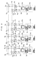
- Fig. 2 is a diagram showing a first embodiment of the optical communication system according to the present invention.
- the terminal equipments A, B, ..., D are connected to each other through optical fiber.
- the terminal equipments A, B, ..., D correspondingly respectively include: driver circuits 1a, 1b, ..., 1d; receiver circuits 2a, 2b, ..., 2d; communication interface sections 3a, 3b, ..., 3d; electro-optic converter sections 4a, 4b, ..., 4d; first branch couplers 5a, 5b, ..., 5d; second branch couplers 6a, 6b, ..., 6d; opto-electric converter sections 7a, 7b, ..., 7d; up-load optical signal input terminals 8a, 8b, ..., 8d; up-load optical signal output terminals 9a, 9b, ..., 9d; down-load optical signal input terminals 10a, 10b, ..., 10d;
- each terminal equipment A B, ..., D
- the communication interface section 3a (3b, ..., 3d) operates together with the driver circuit 1a (1b, ..., 1d) and the receiver circuit 2a (2b, ..., 2d) to perform transmission/reception of an electric signal in accordance with a predetermined communication protocol.
- a transmission signal is converted into an optical signal by the electro-optic converter section 4a (4b, ..., 4d) and a received optical signal is converted into an electric signal by the opto-electric converter section 7a (7a, ..., 7d), the electric signal being led to the receiver circuit 2a (2b, ..., 2d).
- each terminal equipment A (B, ..., D)
- the transmission signal is coupled with an up-load optical signal inputted from the up-load optical signal input terminal 8a (8b, ..., 8d) and then sent out from the up-load optical signal output terminal 9a (9b, ..., 9d).
- the up-load optical signal output terminal 9d of the terminal equipment D is connected to the up-load optical signal input terminal 8c of the terminal equipment C through optical fiber. The same applies to all the terminal equipments so that optical signals transmitted from all of the terminal equipments are sent out from the up-load optical signal output terminal 9a of the terminal equipment A located in the head position.
- the up-load optical signal output terminal 9a of the terminal equipment A is connected to the down-load optical signal input terminal 10a of the terminal equipment A through optical fiber, so that the signals transmitted from all of the terminal equipments are inputted to the down-load optical signal input terminal 10a as a down-load optical signal.
- each terminal equipment A (B, ..., D)
- a signal inputted through the down-load optical signal input terminal 10a (10b, ..., 10d) is branched into two by the second branch coupler 6a (6b, ..., 6d) so that one of the branched signals is sent out from the down-load optical signal output terminal 11a (11b, ..., 11d) and the other is led to the receiver circuit 2a (2b, ..., 2d) after converted into an electric signal by the opto-electric converter section 7a (7b, ..., 7d).
- the down-load optical signal output terminal 11a of the terminal equipment A is connected to the down-load optical signal input terminal 10b of the terminal equipment B through optical fiber.
- each terminal equipment A (B, ..., D) transmits a packet addressed to its own.
- the gain of the optical amplifier 12a (12b, ..., 12d) is started from its minimum.
- the packet addressed to its own is transmitted again after the amplification factor of the optical amplifier 12a (12b, ..., 12d) is increased by one rank. The aforementioned operation is repeated till reception is enabled.
- the signal sent out from the optical amplifier 12a (12b, ..., 12d) in each terminal equipment A (B, ..., D) is attenuated because of losses such as a branching loss, a coupling loss, an insertion loss, and a transmission loss of optical fiber, and then reaches to a reception point.
- the signal sent out of the optical amplifier 12a of the terminal equipment A is passed through the branch couplers 5a and 6a.
- the signal sent out of the optical amplifier 12d of the terminal equipment D is passed through the branch couplers 5d, 5c, 5b, 5a, 6a, 6b, 6c and 6d. Accordingly, in Fig.
- the amplification factor of the terminal equipment A may be set to be the smallest value and, on the other hand, the amplification factor of the terminal equipment D must be set to be the largest value.
- data communications between all of the terminal equipments can be made with no problem if the amplification factors of the all terminal equipments have the same value as the amplification factor of the terminal equipment D.
- each terminal equipment informs the other terminal equipments of its own amplification factor by means of a broadcast packet, and each terminal equipment sets the amplification factor of its own optical amplifier to be the largest value of the amplification factors received through the broadcast packet.
- Fig. 3 shows a second embodiment of the optical communication system according to the present invention.
- the reference numerals 13a, 13b, ..., 13d designate counting means for counting the time difference between the time when a signal is transmitted from the communication interface section 3a (3b, ..., 3d) to the driver circuit 1a (1b, ..., 1d) in the case of packet transmission and the time when an acknowledge bit reaches the communication interface section 3a (3b, ..., 3d) through the receiver circuit 2a (2b, ..., 2d), and for reporting he result of the counting to the communication interface section 3a, (3b, ..., 3d).
- the reference numerals 14a, 14b, ..., 14d designate indication means.
- Fig. 4 shows the data format in a digital data bus.
- the symbol P in the format represents a parity bit, A an acknowledge bit and EOD an end-of-data bit.
- the digital data bus is synchronized based on a start bit and then channel access control by CSMA/CD is performed based on mode and master address bits following the start bit. Consequently, one terminal equipment remaining undefeated acquires priority and transmits parity bits, slave address bits, control bits, data bits and an end-of-data bit as a master.
- An acknowledge bit is the bit for reporting the fact that a terminal equipment designated by the slave address bits has acknowledged information coming to the terminal equipment.
- the designated terminal equipment transmits with the passage of a predetermined time after the terminal equipment receives a bit synchronizing signal transmitted from the master in the early stage of the period of the respective acknowledge bit.
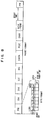
- Fig. 5 shows the bit format of the acknowledge bit.
- the diagram (a) shows a bit synchronizing signal for the acknowledge bit transmitted by the terminal equipment A as a master
- the diagram (b) shows the state where the bit synchronizing signal of the diagram (a) reaches the output of the receiver circuit 2d of the terminal equipment D as a slave.
- the signal of the diagram (b) is delayed, compared with the signal of the diagram (a), for the sum T DA-D of the delay time in the driver circuit 1a and the electro-optic converter section 4a of the terminal equipment A, the delay time in the light transmission line leading from the output point of the electro-optic converter section 4a to the input of the opto-electric converter section 7d of the terminal equipment D and the delay time in the opto-electric converter section 7d and the receiver circuit 2d.
- the acknowledge signal reaches the master in the form of an acknowledge signal shown in the diagram (d) after the signal is delayed for the sum T DD-A of the delay time in the driver circuit 1d and the electro-optic converter section 4d of the terminal equipment D, the delay time in the light transmission line leading from the output point of the electro-optic converter section 4d to the input of the opto-electric converter section 7a of the terminal equipment A and the delay time in the opto-electric converter section 7a and the receiver circuit 2a.
- the one-cycle transmission delay time between the terminal equipments can be found by counting the time difference T D between the point of time when the master transmits a high-level signal with the passage of time T M after transmitting a bit synchronizing signal and the point of time when the master receives an acknowledge signal from the slave.
- the terminal equipment to which a transmission request is given transmits a packet after confirming that a vacant channel exists.
- each terminal equipment transmits mode bits and mater address bits synchronously with the terminal equipment which has transmitted the start bit at the first time.
- Each terminal equipment receives bits and compares the received bits with the bits which the terminal equipment has transmitted. When the result of comparison is discord, the terminal equipment stops signal transmission.
- the system is configured so that, in the case where a high-level bit and a low-level bit collide with each other, the result is made to be low-level, that is priority is given to the low-level bit. Accordingly, a terminal equipment which has transmitted the mode and master address bits containing the greatest number of low-level bits acquires channel access priority to serve as a master.
- FIG. 7 The bit format of the mode and master address bits is shown in Fig. 7.
- the diagram (a) shows the bit format for a terminal equipment to which a transmission request is given and the diagram (b) shows the bit format for a terminal equipment to which no transmission request is given.
- a terminal equipment to which a transmission request is given transmits a bit data of high- or low-level signal for a time period t3 with a passage of time t2 after receiving the bit synchronizing signal which is transmitted with a passage of time t1 after the start bit of the terminal equipment which has transmitted the start bit at the first time is terminated.
- Each terminal equipment A (B, ..., D) performs sampling of the output signal of the receiver circuit 2a (2b, ..., 2d) with a passage of time t S from the bit synchronizing signal.
- T D the one-cycle transmission delay time
- the bit data of the terminal equipment which has transmitted the bit synchronizing signal is not settled before the time t2 + T D is passed after the bit synchronizing signal is transmitted.
- the time t S to the sampling point must satisfies the relation t S > t2 + T D .
- T D 0, the bit data becomes unsettled again after the time t2 + t3.
- the sampling point must be established to satisfy the relation t2 + T D ⁇ t S ⁇ t2 + t3 in which the range of the one-cycle delay time T D must satisfies the relation 0 ⁇ T D ⁇ t3 to make it possible to sample settled data even in the case of t S ⁇ t2 + t3.
- t3 is small and high speed properties are required for the driver circuit 1a (1b, ..., 1d), the receiver circuit 2a (2b, ..., 2d), the electro-optic converter circuit 4a (4b, ..., 4d) and the opto-electric converter circuit 7a (7b, ..., 7d).
- each terminal equipment A (B, ..., D) contains one driver circuit 1a (1b, ..., 1d), one receiver circuit 2a (2b, ..., 2d), one electro-optic converter circuit 4a (4b, ..., 4d) and one opto-electric converter circuit 7a (7b, ..., 7d) as shown in Fig. 3, so that the delay time is considered to be the same even in the case where a communication is made between arbitrary terminal equipments.
- the delay time is represented by T DT
- the one-cycle transmission delay time T D can be represented by the sum of the delay time T DT and the delay time T Do in the optical transmission line.
- settled data can be sampled regardless of the delay time caused by the driver circuit 1a (1b, ..., 1d), the receiver circuit 2a (2b, ..., 2d), the electro-optic converter circuit 4a (4b, ..., 4d) and the opto-electric converter circuit 7a (7b, ..., 7d) constituting the terminal equipment A (B, ..., D) if the delay time caused by the light transmission line is less than the bit length with settled data.
- the system can be modified as follows, and reliability on the system can be improved by the modification.
- the system is designed to report the fact to terminal equipments having delay time T Do more than the bit length t3 so that signal transmission stops and abnormality is reported to the user by any indication means.
- the packet format of the home bus system is shown in Fig. 8.
- the symbol PR in the format represents a priority code, SA a source address, DA a destination address, CC a control code, BC a telegram-length code, DATA data, FCC a check code, DMY a dummy, and ACK/NAK an acknowledge code.
- the home bus system employs start-stop synchronization in which synchronization is made based on the start bit and the stop bit contained in each byte as a constituent member of a packet.
- a terminal equipment designated by the destination address DA returns an acknowledge code with the passage of dummy time (time corresponding to 11 bits) after the terminal equipment receives the packet till the check code FCC.
- the one-cycle transmission delay time T D can be found by subtracting the time corresponding to 11 bits from the value obtained by counting the time difference between the point of time when transmission of the stop bit of the check code is terminated in the terminal equipment to transmit a packet and the point of time when reception of the start bit of the acknowledge code from the other terminal equipment is started.
- channel access control is made based on the respective bits of the priority code and the source address.
- start-stop synchronization as in the home bus system regardless of bit synchronization, it is general that sampling is made in the center of the bit with settled data. In the case where pulse duty ratio is 50%, sampling is made in the point of 1/4 bit length of the respective bit.
- sampling is made in the point of 1/2 bit length of the respective bit.
- the limit of the one-cycle transmission delay time T D is 1/4 bit time in the case where pulse duty ratio is 50%.
- the limit of the one-cycle transmission delay time T D is 1/2 bit time in the case where pulse duty ratio is 100%. Accordingly, the scale of the system is limited more greatly as transmission rate increases.
- sampling timing can be shifted by the mean delay time in the distribution of the transmission delay time through founding the transmission delay time of each terminal equipment according to the method of the invention, so that the permissible range of the one-cycle transmission delay time can be enlarged greatly.
Abstract
Description
- The present invention relates to an optical communication system for realizing a digital data bus for performing information communication between audio and video appliances.
- Fig. 1 shows an example of a system construction of a digital data bus realized by electric communication using metallic with as a transmission medium.
- In Fig. 1, portions surrounded by broken lines designate terminal equipments which are connected to each other through metallic wire. In each terminal equipment, the
reference numeral 3 designates a communication interface section for performing data communication according to a predetermined communication protocol. Adriver circuit 1 and areceiver circuit 2 are connected to thecommunication interface section 3. Thereference numerals reference numeral 17 designates terminal resistors which are provided on opposite ends of the bus for the purpose of impedance matching. - In the case of a digital data bus, wiring between terminal equipments becomes complex, because a data communication transmission medium must be newly provided in addition to a conventional medium for transmitting audio and video signals. Therefore, each terminal equipment may be constituted by a coupler for coupling a transmission signal with an up-load signal and a branch device for branching a reception signal from a down-load signal by use of optical fiber as a transmission medium to thereby facilitate multiple transmission of audio and video signals as well as digital data and saving of wiring between terminal equipments. However, a large insertion loss occurs in the branch device as well as in the coupler, so that the levels of signals between terminal equipments vary widely in the case of bus connection. Further, increase of signal delay time is caused by an opto-electric converter section and an electro-optic converter section, so that there has been a limitation in transmission rate, in number of terminal equipments and in line length for realizing channel access control based on the surviving type CSMA/CD.
- An object of the invention is to provide an optical communication system for realizing a digital data bus in which the aforementioned problems are solved.
- To attain the foregoing object, according to the present invention, the light sending-out level in each terminal equipment is made variable and each terminal equipment measures a packet transmitted by the terminal equipment per se and informs the other terminal equipments of the result of the measurement so that each terminal equipment sets its sending-out level to the largest value of the sending-out levels of which the terminal equipment has been informed.
- Further, each terminal equipment measures the delay time of an acknowledge bit transmitted from the other terminal equipments so that each terminal equipment shifts a sampling point by the mean value of the measured delay time.
- According to the present invention, bus connection of terminal equipments through optical fiber can be made easy, and at the same time, channel access control based on the surviving type CSMA/CD can be made. Furthermore, multiple transmission of audio and video signals as well as digital data and saving of wiring between terminal equipments can be attained.
- The above and other objects, features and advantages of the present invention will be apparent from the following description of the preferred embodiments of the invention taken in connection with the accompanying drawings, wherein:
- Fig. 1 is a configuration diagram of a conventional digital data bus;
- Fig. 2 is a configuration diagram showing a first embodiment of the present invention;
- Fig. 3 is a configuration diagram showing a second embodiment of the present invention;
- Fig. 4 is a diagram for explaining the packet format in a digital data bus;
- Fig. 5 is a diagram for explaining the bit format of an acknowledge bit in a digital data bus;
- Fig. 6 is a diagram for explaining the case where an acknowledge bit is transmitted and received between terminal equipments;
- Fig. 7 is a diagram for explaining the bit format of a mode bit and a master address bit in a digital data bus;
- Fig. 8 is a diagram for explaining the packet format and the byte format in a home-bus system.
- Fig. 2 is a diagram showing a first embodiment of the optical communication system according to the present invention. In Fig. 2, portions surrounded by broken lines designate terminal equipments. The terminal equipments A, B, ..., D are connected to each other through optical fiber. The terminal equipments A, B, ..., D correspondingly respectively include: driver circuits 1a, 1b, ..., 1d;
receiver circuits communication interface sections optic converter sections first branch couplers second branch couplers electric converter sections signal input terminals signal output terminals signal input terminals 10a, 10b, ..., 10d; down-load optical signal output terminals 11a, 11b, ..., 11d; andoptical amplifiers 12a, 12b, ..., 12d in which the amplification factors can be set based on signals sent from the respectivecommunication interface sections - In the following, the construction of the invention is described more in detail. In each terminal equipment A (B, ..., D) the
communication interface section 3a (3b, ..., 3d) operates together with the driver circuit 1a (1b, ..., 1d) and thereceiver circuit 2a (2b, ..., 2d) to perform transmission/reception of an electric signal in accordance with a predetermined communication protocol. A transmission signal is converted into an optical signal by the electro-optic converter section 4a (4b, ..., 4d) and a received optical signal is converted into an electric signal by the opto-electric converter section 7a (7a, ..., 7d), the electric signal being led to thereceiver circuit 2a (2b, ..., 2d). In each terminal equipment A (B, ..., D), the transmission signal is coupled with an up-load optical signal inputted from the up-load opticalsignal input terminal 8a (8b, ..., 8d) and then sent out from the up-load opticalsignal output terminal 9a (9b, ..., 9d). In Fig. 2, the up-load opticalsignal output terminal 9d of the terminal equipment D is connected to the up-load opticalsignal input terminal 8c of the terminal equipment C through optical fiber. The same applies to all the terminal equipments so that optical signals transmitted from all of the terminal equipments are sent out from the up-load opticalsignal output terminal 9a of the terminal equipment A located in the head position. The up-load opticalsignal output terminal 9a of the terminal equipment A is connected to the down-load opticalsignal input terminal 10a of the terminal equipment A through optical fiber, so that the signals transmitted from all of the terminal equipments are inputted to the down-load opticalsignal input terminal 10a as a down-load optical signal. In each terminal equipment A (B, ..., D), a signal inputted through the down-load opticalsignal input terminal 10a (10b, ..., 10d) is branched into two by thesecond branch coupler 6a (6b, ..., 6d) so that one of the branched signals is sent out from the down-load optical signal output terminal 11a (11b, ..., 11d) and the other is led to thereceiver circuit 2a (2b, ..., 2d) after converted into an electric signal by the opto-electric converter section 7a (7b, ..., 7d). In Fig. 2, the down-load optical signal output terminal 11a of the terminal equipment A is connected to the down-load optical signal input terminal 10b of the terminal equipment B through optical fiber. The same applies to all of the terminal equipments so that optical signals transmitted from all of the terminal equipments are led to thereceiver circuit 2a (2b, ..., 2d) of each terminal equipment A (B, ..., D). - In the following, the operation of the system is described.
- At the time of the starting of the system, each terminal equipment A (B, ..., D) transmits a packet addressed to its own. At this time, the gain of the optical amplifier 12a (12b, ..., 12d) is started from its minimum. When the transmitted packet cannot be received, the packet addressed to its own is transmitted again after the amplification factor of the optical amplifier 12a (12b, ..., 12d) is increased by one rank. The aforementioned operation is repeated till reception is enabled.
- The signal sent out from the optical amplifier 12a (12b, ..., 12d) in each terminal equipment A (B, ..., D) is attenuated because of losses such as a branching loss, a coupling loss, an insertion loss, and a transmission loss of optical fiber, and then reaches to a reception point. For example, the signal sent out of the optical amplifier 12a of the terminal equipment A is passed through the
branch couplers optical amplifier 12d of the terminal equipment D is passed through thebranch couplers - Then, each terminal equipment informs the other terminal equipments of its own amplification factor by means of a broadcast packet, and each terminal equipment sets the amplification factor of its own optical amplifier to be the largest value of the amplification factors received through the broadcast packet.
- By the aforementioned configuration, data communication can be made with optimum light intensity corresponding to the scale of the system. Thus, a system excellent in extension, durability and power saving can be realized.
- Fig. 3 shows a second embodiment of the optical communication system according to the present invention. In Fig. 3, the same constituent members as those in the first embodiment shown in Fig. 2 are referenced correspondingly. The
reference numerals 13a, 13b, ..., 13d designate counting means for counting the time difference between the time when a signal is transmitted from thecommunication interface section 3a (3b, ..., 3d) to the driver circuit 1a (1b, ..., 1d) in the case of packet transmission and the time when an acknowledge bit reaches thecommunication interface section 3a (3b, ..., 3d) through thereceiver circuit 2a (2b, ..., 2d), and for reporting he result of the counting to thecommunication interface section 3a, (3b, ..., 3d). Thereference numerals 14a, 14b, ..., 14d designate indication means. - In the following, the operation of the system is described.
- Fig. 4 shows the data format in a digital data bus. In Fig. 4, the symbol P in the format represents a parity bit, A an acknowledge bit and EOD an end-of-data bit. The digital data bus is synchronized based on a start bit and then channel access control by CSMA/CD is performed based on mode and master address bits following the start bit. Consequently, one terminal equipment remaining undefeated acquires priority and transmits parity bits, slave address bits, control bits, data bits and an end-of-data bit as a master. An acknowledge bit is the bit for reporting the fact that a terminal equipment designated by the slave address bits has acknowledged information coming to the terminal equipment. The designated terminal equipment transmits with the passage of a predetermined time after the terminal equipment receives a bit synchronizing signal transmitted from the master in the early stage of the period of the respective acknowledge bit.
- Fig. 5 shows the bit format of the acknowledge bit. Assuming now that the period of time TM from the point of time when the master transmits a bit synchronizing signal to the point of time when the master transmits a high-level signal again is equal to the period of time TS from the point of time when the slave receives the synchronizing signal to the point of time when the slave transmits an acknowledge bit, then the operation of the system is as shown in Fig. 6 in the case where the terminal equipment A as a master in Fig. 3 transmits a bit synchronizing signal and the terminal equipment D as a slave returns an acknowledge signal.
- In Fig. 6, the diagram (a) shows a bit synchronizing signal for the acknowledge bit transmitted by the terminal equipment A as a master, and the diagram (b) shows the state where the bit synchronizing signal of the diagram (a) reaches the output of the
receiver circuit 2d of the terminal equipment D as a slave. The signal of the diagram (b) is delayed, compared with the signal of the diagram (a), for the sum TDA-D of the delay time in the driver circuit 1a and the electro-optic converter section 4a of the terminal equipment A, the delay time in the light transmission line leading from the output point of the electro-optic converter section 4a to the input of the opto-electric converter section 7d of the terminal equipment D and the delay time in the opto-electric converter section 7d and thereceiver circuit 2d. In Fig. 6, the diagram (c) shows an acknowledge signal transmitted by the terminal equipment D with the passage of a predetermined time TS (= TM) after the terminal equipment D receives the bit synchronizing signal. The acknowledge signal reaches the master in the form of an acknowledge signal shown in the diagram (d) after the signal is delayed for the sum TDD-A of the delay time in the driver circuit 1d and the electro-optic converter section 4d of the terminal equipment D, the delay time in the light transmission line leading from the output point of the electro-optic converter section 4d to the input of the opto-electric converter section 7a of the terminal equipment A and the delay time in the opto-electric converter section 7a and thereceiver circuit 2a. In short, the one-cycle transmission delay time between the terminal equipments can be found by counting the time difference TD between the point of time when the master transmits a high-level signal with the passage of time TM after transmitting a bit synchronizing signal and the point of time when the master receives an acknowledge signal from the slave. - In the following, channel access control by the surviving type CSMA/CD is described. The terminal equipment to which a transmission request is given transmits a packet after confirming that a vacant channel exists. In the case where a plurality of terminal equipments try to transmit signals at a time, each terminal equipment transmits mode bits and mater address bits synchronously with the terminal equipment which has transmitted the start bit at the first time. Each terminal equipment receives bits and compares the received bits with the bits which the terminal equipment has transmitted. When the result of comparison is discord, the terminal equipment stops signal transmission. The system is configured so that, in the case where a high-level bit and a low-level bit collide with each other, the result is made to be low-level, that is priority is given to the low-level bit. Accordingly, a terminal equipment which has transmitted the mode and master address bits containing the greatest number of low-level bits acquires channel access priority to serve as a master.
- The bit format of the mode and master address bits is shown in Fig. 7. In Fig. 7, the diagram (a) shows the bit format for a terminal equipment to which a transmission request is given and the diagram (b) shows the bit format for a terminal equipment to which no transmission request is given. A terminal equipment to which a transmission request is given transmits a bit data of high- or low-level signal for a time period t₃ with a passage of time t₂ after receiving the bit synchronizing signal which is transmitted with a passage of time t₁ after the start bit of the terminal equipment which has transmitted the start bit at the first time is terminated. Each terminal equipment A (B, ..., D) performs sampling of the output signal of the
receiver circuit 2a (2b, ..., 2d) with a passage of time tS from the bit synchronizing signal. Under the consideration that the one-cycle transmission delay time TD is between terminal equipments, the bit data of the terminal equipment which has transmitted the bit synchronizing signal is not settled before the time t₂ + TD is passed after the bit synchronizing signal is transmitted. Accordingly, the time tS to the sampling point must satisfies the relation tS > t₂ + TD. In the case of TD = 0, the bit data becomes unsettled again after the time t₂ + t₃. Accordingly, the sampling point must be established to satisfy the relation t₂ + TD < tS < t₂ + t₃ in which the range of the one-cycle delay time TD must satisfies the relation 0 ≦ TD < t₃ to make it possible to sample settled data even in the case of tS ≒ t₂ + t₃. Generally in the case where transmission rate is high, t₃ is small and high speed properties are required for the driver circuit 1a (1b, ..., 1d), thereceiver circuit 2a (2b, ..., 2d), the electro-optic converter circuit 4a (4b, ..., 4d) and the opto-electric converter circuit 7a (7b, ..., 7d). In the configuration of the optical communication system according to the present invention, each terminal equipment A (B, ..., D) contains one driver circuit 1a (1b, ..., 1d), onereceiver circuit 2a (2b, ..., 2d), one electro-optic converter circuit 4a (4b, ..., 4d) and one opto-electric converter circuit 7a (7b, ..., 7d) as shown in Fig. 3, so that the delay time is considered to be the same even in the case where a communication is made between arbitrary terminal equipments. When the delay time is represented by TDT, the one-cycle transmission delay time TD can be represented by the sum of the delay time TDT and the delay time TDo in the optical transmission line. In short, the distribution of the one-cycle transmission delay time TD is represented by the relation TDT < TD ≦ TDT + TDo, and the center of the distribution is TDT + TDo/2. Accordingly, settled data can be sampled regardless of the value of TDT, if TDo is within the range of TDo ≦ t₃, and if the distribution of the one-cycle transmission delay time TD is counted by the counting means in accordance with the present invention to shift the sampling point tS by the result ΔtS (= TTD + TDo/2-t3/2) obtained by subtracting the half (= t3/2) of the bit length t₃ with settled data from the calculated center of the distribution (= TDT + TDo/2). In short, according to the present invention, settled data can be sampled regardless of the delay time caused by the driver circuit 1a (1b, ..., 1d), thereceiver circuit 2a (2b, ..., 2d), the electro-optic converter circuit 4a (4b, ..., 4d) and the opto-electric converter circuit 7a (7b, ..., 7d) constituting the terminal equipment A (B, ..., D) if the delay time caused by the light transmission line is less than the bit length with settled data. Further, the system can be modified as follows, and reliability on the system can be improved by the modification. In the case where the delay time TDo caused by the light transmission line is counted to be more than the bit length t₃ with settled data, the system is designed to report the fact to terminal equipments having delay time TDo more than the bit length t₃ so that signal transmission stops and abnormality is reported to the user by any indication means. - Although the aforementioned embodiments have shown the case where the invention is applied to a digital data bus, the following description shows the case where the invention is applied to a system, such as a home bus system, in which an acknowledge byte is returned after one packet is received.
- The packet format of the home bus system is shown in Fig. 8. In Fig. 8, the symbol PR in the format represents a priority code, SA a source address, DA a destination address, CC a control code, BC a telegram-length code, DATA data, FCC a check code, DMY a dummy, and ACK/NAK an acknowledge code. The home bus system employs start-stop synchronization in which synchronization is made based on the start bit and the stop bit contained in each byte as a constituent member of a packet. A terminal equipment designated by the destination address DA returns an acknowledge code with the passage of dummy time (time corresponding to 11 bits) after the terminal equipment receives the packet till the check code FCC. Accordingly, the one-cycle transmission delay time TD can be found by subtracting the time corresponding to 11 bits from the value obtained by counting the time difference between the point of time when transmission of the stop bit of the check code is terminated in the terminal equipment to transmit a packet and the point of time when reception of the start bit of the acknowledge code from the other terminal equipment is started. In the case of the home bus system, channel access control is made based on the respective bits of the priority code and the source address. In the case of start-stop synchronization as in the home bus system regardless of bit synchronization, it is general that sampling is made in the center of the bit with settled data. In the case where pulse duty ratio is 50%, sampling is made in the point of 1/4 bit length of the respective bit. In the case where pulse duty ratio is 100%, sampling is made in the point of 1/2 bit length of the respective bit. Accordingly, the limit of the one-cycle transmission delay time TD is 1/4 bit time in the case where pulse duty ratio is 50%. The limit of the one-cycle transmission delay time TD is 1/2 bit time in the case where pulse duty ratio is 100%. Accordingly, the scale of the system is limited more greatly as transmission rate increases. According to the method of the invention, sampling timing can be shifted by the mean delay time in the distribution of the transmission delay time through founding the transmission delay time of each terminal equipment according to the method of the invention, so that the permissible range of the one-cycle transmission delay time can be enlarged greatly.
Claims (4)
Applications Claiming Priority (2)
| Application Number | Priority Date | Filing Date | Title |
|---|---|---|---|
| JP17992/89 | 1989-01-27 | ||
| JP1017992A JPH02199942A (en) | 1989-01-27 | 1989-01-27 | Optical communication equipment |
Publications (3)
| Publication Number | Publication Date |
|---|---|
| EP0380341A2 true EP0380341A2 (en) | 1990-08-01 |
| EP0380341A3 EP0380341A3 (en) | 1991-10-02 |
| EP0380341B1 EP0380341B1 (en) | 1995-09-13 |
Family
ID=11959222
Family Applications (1)
| Application Number | Title | Priority Date | Filing Date |
|---|---|---|---|
| EP90300797A Expired - Lifetime EP0380341B1 (en) | 1989-01-27 | 1990-01-25 | Optical communication system |
Country Status (4)
| Country | Link |
|---|---|
| US (1) | US5046137A (en) |
| EP (1) | EP0380341B1 (en) |
| JP (1) | JPH02199942A (en) |
| DE (1) | DE69022256T2 (en) |
Cited By (4)
| Publication number | Priority date | Publication date | Assignee | Title |
|---|---|---|---|---|
| US5130836A (en) * | 1990-06-01 | 1992-07-14 | Japan Aviation Electronics Industry Limited | Optical transceiver |
| WO2004030244A1 (en) * | 2002-09-27 | 2004-04-08 | Lockheed Martin Corporation | Optical distribution network for rf and other analog signals |
| WO2004093351A2 (en) * | 2003-03-31 | 2004-10-28 | Lockheed Martin Corporation | Optical network interface systems and devices |
| USRE41247E1 (en) | 1997-04-01 | 2010-04-20 | Lockheed Martin Corporation | Optical transport system |
Families Citing this family (16)
| Publication number | Priority date | Publication date | Assignee | Title |
|---|---|---|---|---|
| US5109532A (en) * | 1990-01-30 | 1992-04-28 | General Instrument Corporation | Elimination of phase noise and drift incident to up and down conversion in a broadcast communication system |
| DE4139300A1 (en) * | 1991-11-29 | 1993-06-03 | Rheydt Kabelwerk Ag | Network topology for bidirectional data transmission in passive network - has cable branch points at beginning and end of network dividing central device data lines into local device data lines |
| US5809187A (en) * | 1997-04-24 | 1998-09-15 | Boeing North American, Inc. | Multi-port network using passive optical couplers |
| KR100607943B1 (en) * | 1999-11-15 | 2006-08-03 | 삼성전자주식회사 | Apparatus and method for bus interface for optical module |
| US20030053166A1 (en) * | 2001-09-14 | 2003-03-20 | Hamm Russell O. | Method and apparatus of transmitting several digital signals over a common optical fiber |
| US7085497B2 (en) | 2002-04-03 | 2006-08-01 | Lockheed Martin Corporation | Vehicular communication system |
| US6912339B2 (en) * | 2002-09-27 | 2005-06-28 | Lockheed Martin Corporation | Optical interface devices having balanced amplification |
| US7283480B1 (en) | 2002-11-12 | 2007-10-16 | Lockheed Martin Corporation | Network system health monitoring using cantor set signals |
| US7349629B1 (en) | 2002-11-26 | 2008-03-25 | Lockheed Martin Corporation | Methods and systems for creating a digital interconnect fabric |
| US7424228B1 (en) | 2003-03-31 | 2008-09-09 | Lockheed Martin Corporation | High dynamic range radio frequency to optical link |
| US7440699B1 (en) | 2004-06-28 | 2008-10-21 | Lockheed Martin Corporation | Systems, devices and methods for transmitting and receiving signals on an optical network |
| WO2009022672A1 (en) * | 2007-08-10 | 2009-02-19 | Nec Corporation | Optical data bus and optical data transmission system using the same |
| JP2011049964A (en) * | 2009-08-28 | 2011-03-10 | Denso Corp | Node used for communication system |
| CN103378905B (en) * | 2012-04-27 | 2017-02-08 | 鸿富锦精密工业(深圳)有限公司 | Optical fiber transmission system |
| CN103457662A (en) * | 2012-05-28 | 2013-12-18 | 鸿富锦精密工业(深圳)有限公司 | Optical fiber transmission system |
| CN112861364B (en) * | 2021-02-23 | 2022-08-26 | 哈尔滨工业大学(威海) | Method for realizing anomaly detection by modeling industrial control system equipment behavior based on secondary annotation of state delay transition diagram |
Citations (3)
| Publication number | Priority date | Publication date | Assignee | Title |
|---|---|---|---|---|
| WO1984004638A1 (en) * | 1983-05-12 | 1984-11-22 | American Telephone & Telegraph | Communication network |
| EP0216214A2 (en) * | 1985-09-25 | 1987-04-01 | Siemens Aktiengesellschaft | Method for the automatic level adjustment in a local area network, in particular for a multiprocessor arrangement with a bus system of optical fibres, for the purpose of collision detection |
| EP0224132A2 (en) * | 1985-11-13 | 1987-06-03 | Fujitsu Limited | Optical composite transceiver |
Family Cites Families (2)
| Publication number | Priority date | Publication date | Assignee | Title |
|---|---|---|---|---|
| JPS5857835A (en) * | 1981-09-30 | 1983-04-06 | Yokogawa Hokushin Electric Corp | Optical communication system |
| US4742576A (en) * | 1985-12-23 | 1988-05-03 | Polaroid Corporation | Optical communication system employing coherent detection and method |
-
1989
- 1989-01-27 JP JP1017992A patent/JPH02199942A/en active Pending
-
1990
- 1990-01-23 US US07/469,065 patent/US5046137A/en not_active Expired - Fee Related
- 1990-01-25 DE DE69022256T patent/DE69022256T2/en not_active Expired - Fee Related
- 1990-01-25 EP EP90300797A patent/EP0380341B1/en not_active Expired - Lifetime
Patent Citations (3)
| Publication number | Priority date | Publication date | Assignee | Title |
|---|---|---|---|---|
| WO1984004638A1 (en) * | 1983-05-12 | 1984-11-22 | American Telephone & Telegraph | Communication network |
| EP0216214A2 (en) * | 1985-09-25 | 1987-04-01 | Siemens Aktiengesellschaft | Method for the automatic level adjustment in a local area network, in particular for a multiprocessor arrangement with a bus system of optical fibres, for the purpose of collision detection |
| EP0224132A2 (en) * | 1985-11-13 | 1987-06-03 | Fujitsu Limited | Optical composite transceiver |
Non-Patent Citations (3)
| Title |
|---|
| FUJITSU SCIENTIFIC & TECHNICAL JOURNAL, vol. 21, no. 4, September 1985, pages 436-443, Kawasaki, JP; S. SANO et al.: "Optical bus-LAN conforming to IEEE 802 (CSMA/CD)" * |
| IEEE JOURNAL ON SELECTED AREAS IN COMMUNICATIONS, vol. SAC-3, no. 6, November 1985, pages 890-896, New York, US; J.W. REEDY et al.: "Methods of collision detection in fiber optic CSMA/CD networks" * |
| IEEE TRANSACTIONS ON COMMUNICATIONS, vol. COM-35, no. 4, April 1987, pages 419-426, New York, US; S.S. WAGNER: "Optical amplifier applications in fiber optic local networks" * |
Cited By (5)
| Publication number | Priority date | Publication date | Assignee | Title |
|---|---|---|---|---|
| US5130836A (en) * | 1990-06-01 | 1992-07-14 | Japan Aviation Electronics Industry Limited | Optical transceiver |
| USRE41247E1 (en) | 1997-04-01 | 2010-04-20 | Lockheed Martin Corporation | Optical transport system |
| WO2004030244A1 (en) * | 2002-09-27 | 2004-04-08 | Lockheed Martin Corporation | Optical distribution network for rf and other analog signals |
| WO2004093351A2 (en) * | 2003-03-31 | 2004-10-28 | Lockheed Martin Corporation | Optical network interface systems and devices |
| WO2004093351A3 (en) * | 2003-03-31 | 2005-03-24 | Lockheed Corp | Optical network interface systems and devices |
Also Published As
| Publication number | Publication date |
|---|---|
| JPH02199942A (en) | 1990-08-08 |
| DE69022256T2 (en) | 1996-05-09 |
| EP0380341A3 (en) | 1991-10-02 |
| US5046137A (en) | 1991-09-03 |
| DE69022256D1 (en) | 1995-10-19 |
| EP0380341B1 (en) | 1995-09-13 |
Similar Documents
| Publication | Publication Date | Title |
|---|---|---|
| US5046137A (en) | Optical communication system | |
| EP0110691B1 (en) | System and method for controlling a multiple access data communications system | |
| GB2166328A (en) | In-house distribution facility for a broadband communication system | |
| US4850047A (en) | Optical bus communication system utilizing frame format signals | |
| JP2836592B2 (en) | Optical transceiver and network using the optical transceiver | |
| US4646361A (en) | Optical star repeater | |
| EP0118763A2 (en) | Method of searching fault locations in digital transmission line | |
| GB2128058A (en) | Multiple access data communication system | |
| EP0476444A1 (en) | Optical transceiver | |
| EP0112126A2 (en) | Communication network and method for its use | |
| US4746918A (en) | Split bus system interface | |
| US4288869A (en) | Half-duplex/simplex digital signal converter | |
| EP0568314A2 (en) | Distributed data-processing star network and a concentrator and terminal devices used therein | |
| US4683471A (en) | Data bus pilot tone | |
| JPH0472939A (en) | Packet exchange using optical switch | |
| JP3068125B2 (en) | Bus type optical transmission line communication station | |
| JPH0214823B2 (en) | ||
| KR920007747Y1 (en) | Transmitter/receiver for interfancing local area network | |
| JP2684775B2 (en) | Burst signal reception method | |
| JPS6198041A (en) | Optical transceiver | |
| KR200180537Y1 (en) | Data transceiver for voice message handling in switch | |
| EP0364170A2 (en) | High speed serial data link | |
| EP0517492A1 (en) | Data bus systems | |
| JPH0685796A (en) | Two-wire transmission system | |
| JPH0410266B2 (en) |
Legal Events
| Date | Code | Title | Description |
|---|---|---|---|
| PUAI | Public reference made under article 153(3) epc to a published international application that has entered the european phase |
Free format text: ORIGINAL CODE: 0009012 |
|
| AK | Designated contracting states |
Kind code of ref document: A2 Designated state(s): DE FR GB NL |
|
| RIN1 | Information on inventor provided before grant (corrected) |
Inventor name: MOCHIDA, YOSIHISA Inventor name: SUGINO, NOBUO Inventor name: IKEZAKI, MASAO Inventor name: NAKATSU, HIROMASA Inventor name: KUROBE, AKIO |
|
| 17P | Request for examination filed |
Effective date: 19901228 |
|
| PUAL | Search report despatched |
Free format text: ORIGINAL CODE: 0009013 |
|
| AK | Designated contracting states |
Kind code of ref document: A3 Designated state(s): DE FR GB NL |
|
| 17Q | First examination report despatched |
Effective date: 19940111 |
|
| GRAA | (expected) grant |
Free format text: ORIGINAL CODE: 0009210 |
|
| AK | Designated contracting states |
Kind code of ref document: B1 Designated state(s): DE FR GB NL |
|
| REF | Corresponds to: |
Ref document number: 69022256 Country of ref document: DE Date of ref document: 19951019 |
|
| ET | Fr: translation filed | ||
| PLBE | No opposition filed within time limit |
Free format text: ORIGINAL CODE: 0009261 |
|
| STAA | Information on the status of an ep patent application or granted ep patent |
Free format text: STATUS: NO OPPOSITION FILED WITHIN TIME LIMIT |
|
| 26N | No opposition filed | ||
| REG | Reference to a national code |
Ref country code: GB Ref legal event code: IF02 |
|
| PGFP | Annual fee paid to national office [announced via postgrant information from national office to epo] |
Ref country code: FR Payment date: 20030110 Year of fee payment: 14 |
|
| PGFP | Annual fee paid to national office [announced via postgrant information from national office to epo] |
Ref country code: GB Payment date: 20030122 Year of fee payment: 14 |
|
| PGFP | Annual fee paid to national office [announced via postgrant information from national office to epo] |
Ref country code: NL Payment date: 20030130 Year of fee payment: 14 |
|
| PGFP | Annual fee paid to national office [announced via postgrant information from national office to epo] |
Ref country code: DE Payment date: 20030206 Year of fee payment: 14 |
|
| PG25 | Lapsed in a contracting state [announced via postgrant information from national office to epo] |
Ref country code: GB Free format text: LAPSE BECAUSE OF NON-PAYMENT OF DUE FEES Effective date: 20040125 |
|
| PG25 | Lapsed in a contracting state [announced via postgrant information from national office to epo] |
Ref country code: NL Free format text: LAPSE BECAUSE OF NON-PAYMENT OF DUE FEES Effective date: 20040801 |
|
| PG25 | Lapsed in a contracting state [announced via postgrant information from national office to epo] |
Ref country code: DE Free format text: LAPSE BECAUSE OF NON-PAYMENT OF DUE FEES Effective date: 20040803 |
|
| GBPC | Gb: european patent ceased through non-payment of renewal fee |
Effective date: 20040125 |
|
| PG25 | Lapsed in a contracting state [announced via postgrant information from national office to epo] |
Ref country code: FR Free format text: LAPSE BECAUSE OF NON-PAYMENT OF DUE FEES Effective date: 20040930 |
|
| NLV4 | Nl: lapsed or anulled due to non-payment of the annual fee |
Effective date: 20040801 |
|
| REG | Reference to a national code |
Ref country code: FR Ref legal event code: ST |