EP0379671A2 - Noise reduction for photodiode arrays - Google Patents
Noise reduction for photodiode arrays Download PDFInfo
- Publication number
- EP0379671A2 EP0379671A2 EP89121724A EP89121724A EP0379671A2 EP 0379671 A2 EP0379671 A2 EP 0379671A2 EP 89121724 A EP89121724 A EP 89121724A EP 89121724 A EP89121724 A EP 89121724A EP 0379671 A2 EP0379671 A2 EP 0379671A2
- Authority
- EP
- European Patent Office
- Prior art keywords
- noise
- transfer switch
- signal
- charge amplifier
- photodiode
- Prior art date
- Legal status (The legal status is an assumption and is not a legal conclusion. Google has not performed a legal analysis and makes no representation as to the accuracy of the status listed.)
- Granted
Links
Images


Classifications
-
- H—ELECTRICITY
- H04—ELECTRIC COMMUNICATION TECHNIQUE
- H04N—PICTORIAL COMMUNICATION, e.g. TELEVISION
- H04N25/00—Circuitry of solid-state image sensors [SSIS]; Control thereof
- H04N25/60—Noise processing, e.g. detecting, correcting, reducing or removing noise
- H04N25/616—Noise processing, e.g. detecting, correcting, reducing or removing noise involving a correlated sampling function, e.g. correlated double sampling [CDS] or triple sampling
-
- G—PHYSICS
- G11—INFORMATION STORAGE
- G11C—STATIC STORES
- G11C7/00—Arrangements for writing information into, or reading information out from, a digital store
- G11C7/005—Arrangements for writing information into, or reading information out from, a digital store with combined beam-and individual cell access
-
- H—ELECTRICITY
- H03—ELECTRONIC CIRCUITRY
- H03F—AMPLIFIERS
- H03F3/00—Amplifiers with only discharge tubes or only semiconductor devices as amplifying elements
- H03F3/04—Amplifiers with only discharge tubes or only semiconductor devices as amplifying elements with semiconductor devices only
- H03F3/08—Amplifiers with only discharge tubes or only semiconductor devices as amplifying elements with semiconductor devices only controlled by light
- H03F3/087—Amplifiers with only discharge tubes or only semiconductor devices as amplifying elements with semiconductor devices only controlled by light with IC amplifier blocks
-
- H—ELECTRICITY
- H03—ELECTRONIC CIRCUITRY
- H03F—AMPLIFIERS
- H03F3/00—Amplifiers with only discharge tubes or only semiconductor devices as amplifying elements
- H03F3/70—Charge amplifiers
-
- H—ELECTRICITY
- H04—ELECTRIC COMMUNICATION TECHNIQUE
- H04N—PICTORIAL COMMUNICATION, e.g. TELEVISION
- H04N25/00—Circuitry of solid-state image sensors [SSIS]; Control thereof
- H04N25/60—Noise processing, e.g. detecting, correcting, reducing or removing noise
- H04N25/65—Noise processing, e.g. detecting, correcting, reducing or removing noise applied to reset noise, e.g. KTC noise related to CMOS structures by techniques other than CDS
-
- H—ELECTRICITY
- H04—ELECTRIC COMMUNICATION TECHNIQUE
- H04N—PICTORIAL COMMUNICATION, e.g. TELEVISION
- H04N25/00—Circuitry of solid-state image sensors [SSIS]; Control thereof
- H04N25/70—SSIS architectures; Circuits associated therewith
- H04N25/71—Charge-coupled device [CCD] sensors; Charge-transfer registers specially adapted for CCD sensors
- H04N25/75—Circuitry for providing, modifying or processing image signals from the pixel array
-
- H—ELECTRICITY
- H04—ELECTRIC COMMUNICATION TECHNIQUE
- H04N—PICTORIAL COMMUNICATION, e.g. TELEVISION
- H04N25/00—Circuitry of solid-state image sensors [SSIS]; Control thereof
- H04N25/70—SSIS architectures; Circuits associated therewith
- H04N25/76—Addressed sensors, e.g. MOS or CMOS sensors
Definitions
- This invention relates generalLy to reducing noise in Photodiode Arrays (PDA), and in the preferred embodiment, to improving the performance of a spectrometer which uses a photodiode array detector.
- PDA Photodiode Arrays
- Each pixel consists of a photodiode and an associated storage capacitor which may be the junction capacitance of the photodiode or a physical capacitor incorporated into the PDA.
- the capacitor is charged to a reference voltage and then partially discharged as the photodiode conducts photo current in response to the light signal.
- a number of Field Effect Transistor (FET) transfer switches are coupled in series between each pixel and a charge amplifier.
- FET Field Effect Transistor
- Each pixel may be read out in succession by sequentially turning on, therefore, closing, the associated transfer switch. This action also enables the amplifier to recharge the associated capacitor to the reference voltage.
- the amount of charge required to bring the capacitors up to the reference voltage is defined as the image signal charge and is proportional to the intensity of the light or image incident on the photodiode.
- Sensitivity a measurement of the minimum amount of the image signal or light signal that can be detected, is an important feature of spectrometers used in atomic emission detectors.
- a PDA is used to convert optical emissions into an electronic signal.
- electronic noise generated by the PDA can obscure weak signals. The invention reduces this noise, and thereby improves the overall sensitivity of the spectrometer or other apparatus employing the invention.
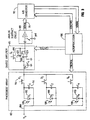
- FIG. 1 shows a conventional PDA 5 connected to a charge amplifier 20.
- One side of each photodiode capacitor pair is coupled to a common node 6.
- serial readout of a charge voltage across each photodiode 13 in the FDA 5 is accomplished by means of a digital shift register (not shown) coupled to the transfer switches 16 (Q1 - Q n ) Operation of this circuit is as follows:
- step 3 the closed loop bandwidth of the integrator amplifier 23 is increased significantly. This results in increased noise charge fluctuations at the inverting input node 99. These fluctuations are due to the input voltage noise of the amplifier as well as thermal noise generated by the reset switch 21. At the instant the reset switch is opened, whatever noise voltage happens to be present on the inverting input node 99 is "frozen" on capacitor 22 (C f ).
- FIG. 1 One prior art technique for reducing this noise is called "correlated double sampling” and employs the analog subtraction circuit 25 shown in Figure 2 and incorporated into Figure 1.
- This circuit consists of a series capacitor 26 and a switch 27 that connects the output end of the capacitor to ground. Switch 27 is turned on just after the integrator amplifier 23 reset operation, and turned off just before the next pixel is connected to the integrator amplifier 23 input. This causes the sum of the amplifier input noise and the thermal noise charges to be stored on capacitor 26, thereby subtracting this term from the output signal. As illustrated in Figure 1, this circuit is coupled to the output of the charge amplifier 20.
- an analog subtract circuit is not required for the detection of light signals in a photodiode array, but it does enhance performance.
- the FET transfer switch 16 (Q1) is another source of thermal noise. This noise is sometimes even greater than the reset switch noise. Unfortunately, The correlated double sampling subtraction technique does not address this problem and overall sensitivity of any device employing the PDA is impaired.
- kTC noise is a type of thermal noise which is caused by random motion of electrons in some eletronic devices, and Field Effect Transitors in particular, and is associated with resetting the photodiode capacitance to a fixed voltage.
- the term kTC stems from Boltzman's constant "k", the temperature "T” and the capacitance "C”.
- this thermal noise charge corresponds to the square root of k*T*C which is technically defined as the Root Mean Square (RMS) noise charge.
- RMS Root Mean Square
- a preferred embodiment of the present invention employs a microprocessor, coupled to a PDA and a low bandwidth charge amplifier, to control the switching or the PDA, which is coupled, through a FET transfer switch to the charge amplifier such that image signal charges and noise charges can be measured and stored for processing.
- the invention measures and stores kTC noise charges generated by the transfer switch.
- image signal denotes a signal which is a representation of, and is generally proportional to, the intensity of the light of the corresponding optical signal.
- this optical signal can be pictorial, as in a camera, spectral, as in a spectrometer or of a different nature.
- the invention is the product of three discoveries which together provide for substantial noise reduction.
- the first discovery was the inventor's realization that the kTC noise charge generated by the transfer switch displaces itself evenly, but with opposite polarity, on the photodiode capacitor and the charge amplifier when the transfer switch is opened.
- the inventor discovered a subtraction technique in which an error signal could be isolated and stored for later subtraction from an image charge signal also containing the unwanted noise, thus providing the desired error-free image charge signal.
- the inventor discovered that by using a low bandwidth amplifier, which does not respond to high frequency noise, it would be possible to take two image charge signal readings for each photodiode during each cycle of the PDA.
- the first reading includes both a first noise charge signal and an image charge signal
- the second reading includes both the first reading and a second noise charge signal.
- the first reading is made with the transfer switch is closed, and the second reading is made after the transfer switch is subsequently opened.
- the amplifier does not respond to the second noise charge signal as it is a high frequency AC signal while the switch is closed. Once the transfer switch is opened, this signal stops changing rapidly and the second reading is made. Therefore, the function of the low bandwidth amplifier is not only to reduce noise at the output, but is also used to enable the charge amplifier to respond to the noise signals so that they can be amplified, measured and subtracted.
- the invention reduces noise in one light sensing circuit, which includes at least a parallel combination of a photodiode and a photodiode capacitor as a pair, or the equivalent thereto, coupled to a low bandwidth charge amplifier through a transfer switch.
- a series of noisy image signals corresponding to an image signal representing the intensity of light incident on the photodiode and an unwanted noise signal, generated by the transfer switch, may be sequentially transferred to the charge amplifier by opening and closing the transfer switch. Such transferred signals may be measured and stored for further processing to eliminate the unwanted noise. Noise reduction may be accomplished by the following steps;
- the present invention is disclosed in Figure 3 and is utilized, in the preferred embodiment, in the input section for a spectrometer.
- incident light 108 is translated into an electronic measure readable by the microprocessor 100.
- the PDA 80 and the charge amplifier 85 operate in a manner similar to that disclosed in the Background of the Invention and illustrated in Figure 1.
- a series of transfer switches 116 (Q1 - Q n ) are employed for coupling each pixel of the PDA 80 to the charge amplifier 85.
- One side of each photodiode capacitor pair in the PDA 80 is coupled to a common node 106.
- a reference voltage V d is also coupled to the circuit at this common node 106.
- the reference voltage of the PDA may vary.
- the invention employs a charge amplifier 85 having a very low bandwidth operational amplifier 123 to limit kTC noise associated with a closed transfer switch 116 while the image charge on the photodiode capacitor 114 is being measured, as well as being able to respond to the kTC noise associated with an opened transfer switch 116 while the noise charge is being measured.
- the switch opened With the switch opened, the kTC noise charge appears as a slowly varying signal, something a low bandwidth amplifier can respond to, as opposed to a rapidly fluctuating AC signal.
- the bandwidth of the amplifier is made sufficiently low such that the time constant of the amplifier is much greater than the time constant RC s , where C s is the series combination of the photodiode capacitor C1 and the total amplifier capacitance C t which consists of the amplifier input capacitance and the capacitance of the feedback capacitor 122.
- C s is the series combination of the photodiode capacitor C1 and the total amplifier capacitance C t which consists of the amplifier input capacitance and the capacitance of the feedback capacitor 122.
- the use of a low bandwidth amplifier provides for making two readings of each photodiode during each cycle of the FDA, and noise reduction through an inventive subtraction technique.
- an operational amplifier having a time constant of approximately 10 microseconds and a 3 dB point of 16 kilohertz was utilized.
- This time constant is more than five times greater than the product of the transfer switch resistance and the series combination of the total amplifier capacitance and the photodiode capacitance. Additionally, the amplifier time constant is less than one fifth of the readout time for each photodiode element of the photodiode array.
- the advantages of this invention stem from the recognition that the kTC noise charge generated by the transfer switch 116 (Q1) is displaced, upon opening of the transfer switch 116 (Q1), evenly (but with opposite polarity) upon the photodiode capacitor 114 (C1 - C n ) and upon the parallel combination of the feedback capacitor 122 (C f ) and the equivalent capacitor 124 (C a ) which represents the input capacitance of the charge amplifier 85 as well as the run capacitance of the PC board.
- This charge distribution not previously appreciated in other photodiode array sampling devices, makes possible the elimination of this kTC noise.
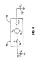
- FIG. 4 depicts a high frequency model of the transfer switch 116 (Q1), the photodiode capacitor 72 (C1) and the total amplifier capacitance 78 (C t ) which is the parallel capacitance of the feedback capacitor 122 (C f ) and the equivalent capacitor 124 (C a ).
- the transfer switch 116 (Q1) of Figure 4 is modeled as a noiseless resistor 74 (R), a resistor noise voltage source 76 (V n ), and an ideal switch 77. This model is only valid at frequencies above the unity gain point of the operational amplifier. At frequencies much greater than the unity gain point of the amplifier, the output of the amplifier remains at a constant voltage.
- the time constant of the charge amplifier is much greater than the RC s time constant composed of the product of the resistor 74 (R) and series capacitance C s of capacitors 72 (C1) and 78 (C t )
- this kTC noise charge is not immediately seen at the output of the operational amplifier because the bandwidth of the amplifier is very low compared to the bandwidth of the noise.
- the transfer switch 116 (Q1) When the transfer switch 116 (Q1) is opened, the feedback capacitor 122 (C f ) receives an additional noise charge.
- the noise charge stored on capacitor 78 (C t ), or equivalently on the inverting input node 198 (see Fig. 3) is transferred completely to the feedback capacitor 122 (C f ) by the action of the operational amplifier 123, so that an additional voltage proportional to the noise charge appears at the output node 197.
- the same noise charge is present (with opposite polarity) on the capacitor 114.
- This noise charge on capacitor 114 remains until the transfer switch 116 (Q1) is again closed.
- a reset switch 199 coupled across capacitor 122, is used for resetting the capacitor between measurments.
- the preferred embodiment of the invention employs an analog subtract circuit 88 to reduce thermal switching noise generated by the reset switch 199.
- This circuit operates in the same manner as the circuit in Figure 2 (which is disclosed in the Background of the Invention).
- an analog subtract circuit is not required, and without it, the output of the charge amplifier could be coupled directly to an A/D converter 90.
- the A/D converter 90 is employed to convert the analog subtract circuit 88 output signal 91 to a digital form.
- the microprocessor 100 controls the FET transfer switches 116 and the reset switch 199 (Q f ) in order to perform kTC noise cancellation on the output signal.
- the following steps describe the operation of one photodiode 110 for one measurement cycle. It is understood that in actual operation, the same steps are performed on each of the photodiodes in the array in exactly the same way, so that a continuous cycling of measurements may be made.
- the preferred embodiment of the invention is illustrated in the following inventive steps:
- the sensitivity of a spectrometer is enhanced.
- the invention has many other applications where kTC noise reduction is required.
- optical character recognition circuits, CCD imagers, image sensors and broadcast cameras are examples of optical character recognition circuits, CCD imagers, image sensors and broadcast cameras. Changes and modification of the invention, as set forth in the specifically described embodiments, can be carried out without departing from the scope of the invention which is intended to be limited only by the scope of the appended claims.
Abstract
Description
- This invention relates generalLy to reducing noise in Photodiode Arrays (PDA), and in the preferred embodiment, to improving the performance of a spectrometer which uses a photodiode array detector. In such a spectrometer, light of different wavelengths is focused on different elements, or pixels, of the PDA. Each pixel consists of a photodiode and an associated storage capacitor which may be the junction capacitance of the photodiode or a physical capacitor incorporated into the PDA. The capacitor is charged to a reference voltage and then partially discharged as the photodiode conducts photo current in response to the light signal. A number of Field Effect Transistor (FET) transfer switches are coupled in series between each pixel and a charge amplifier. Each pixel may be read out in succession by sequentially turning on, therefore, closing, the associated transfer switch. This action also enables the amplifier to recharge the associated capacitor to the reference voltage. The amount of charge required to bring the capacitors up to the reference voltage is defined as the image signal charge and is proportional to the intensity of the light or image incident on the photodiode.
- Sensitivity, a measurement of the minimum amount of the image signal or light signal that can be detected, is an important feature of spectrometers used in atomic emission detectors. To monitor the signal of interest, a PDA is used to convert optical emissions into an electronic signal. During operation, electronic noise generated by the PDA can obscure weak signals. The invention reduces this noise, and thereby improves the overall sensitivity of the spectrometer or other apparatus employing the invention.
- Figure 1 shows a
conventional PDA 5 connected to acharge amplifier 20. One side of each photodiode capacitor pair is coupled to a common node 6. serial readout of a charge voltage across eachphotodiode 13 in the FDA 5 is accomplished by means of a digital shift register (not shown) coupled to the transfer switches 16 (Q₁ - Qn) Operation of this circuit is as follows: - 1. After the previous readout cycle is completed, each pixel capacitor 14 (C₁ - Cn) is charged to a reference voltage Vd. Such charging is carried out by the action of the
operational amplifier 23 as the reference voltage is maintained between its non-inverting input and the common node of the photodiode array. - 2. After the pixel capacitors 14 have been charged, the
transfer switch 16 is opened, so that thephotodiode 13 and pixel capacitor 14 are disconnected from theoperational amplifier 23 for a specified period of time. An optical or light signal 8 is converted to an image signal by the associated photodiode and is integrated on pixel capacitors C₁...Cn, thus discharging each capacitor by an amount of charge representative of the intensity of the optical or light signal 8. The amount of charge removed is defined as the "image signal charge". The term "image signal" is not meant to limit the meaning of "signal" to something corresponding to optical signals which are pictorial in nature. Rather, "image signal" denotes a signal which is a representation of, and is generally proportional to, the intensity of the light of the corresponding optical signal. This optical signal can be either pictorial, as in a camera, or spectral, as in a spectrometer, or of a different nature. The amount of charge removed is defined as the "image signal charge". - 3. Transfer switches 16 (Q₁ - Qn) are employed for successively recharging capacitors 14 (C₁- Cn) by transferring the image signal charge to the inverting input node 99 of the operational amplifier. The operational amplifier acts to keep the voltage on the inverting input node 99 equal to the voltage on the non-inverting input, by changing the voltage on the output node 97 until the input node 99 equals the voltage on the non-inverting input. In this circuit, the non-inverting input, and therefore the inverting input, are equal to ground. Thus, the inverting input is commonly refered to as virtual ground. At this point, all of the of the image signal charge is held on the feedback capacitor 22 (Cf), and none of it is stored on capacitor 24 (Ca), and the voltage at the output node 97 is proportional to the image signal charge. Each pixel may be successively read in this fashion. After reading each pixel, field effect transistor reset switch 21 (Qf) is closed to short out capacitor 22 (Cf), then opened to accept the charge from the next pixel.
- 4. Other circuitry (not shown) reads the value of the image charge signal and stores each reading in a computer memory for processing.
- During the reset operation of the operational amplifier (step 3), the closed loop bandwidth of the
integrator amplifier 23 is increased significantly. This results in increased noise charge fluctuations at the inverting input node 99. These fluctuations are due to the input voltage noise of the amplifier as well as thermal noise generated by thereset switch 21. At the instant the reset switch is opened, whatever noise voltage happens to be present on the inverting input node 99 is "frozen" on capacitor 22 (Cf). - One prior art technique for reducing this noise is called "correlated double sampling" and employs the
analog subtraction circuit 25 shown in Figure 2 and incorporated into Figure 1. This circuit consists of aseries capacitor 26 and aswitch 27 that connects the output end of the capacitor to ground.Switch 27 is turned on just after theintegrator amplifier 23 reset operation, and turned off just before the next pixel is connected to theintegrator amplifier 23 input. This causes the sum of the amplifier input noise and the thermal noise charges to be stored oncapacitor 26, thereby subtracting this term from the output signal. As illustrated in Figure 1, this circuit is coupled to the output of thecharge amplifier 20. However, such an analog subtract circuit is not required for the detection of light signals in a photodiode array, but it does enhance performance. - The FET transfer switch 16 (Q₁) is another source of thermal noise. This noise is sometimes even greater than the reset switch noise. Unfortunately, The correlated double sampling subtraction technique does not address this problem and overall sensitivity of any device employing the PDA is impaired.
- In particular, the switching action of the field effect transistor transfer switch in the integration-readout process causes a noise term, called "kTC" noise, to be unfortunately added to each photodiode measurement. This "kTC" noise is a type of thermal noise which is caused by random motion of electrons in some eletronic devices, and Field Effect Transitors in particular, and is associated with resetting the photodiode capacitance to a fixed voltage. The term kTC stems from Boltzman's constant "k", the temperature "T" and the capacitance "C". In actuality, this thermal noise charge corresponds to the square root of k*T*C which is technically defined as the Root Mean Square (RMS) noise charge. However, this noise charge will hereinafter be identified as "kTC noise". When PDA's are operated at low light levels, this kTC noise is often the largest noise term. It is the purpose of this invention to eliminate this KTC noise.
- Accordingly, it is the object of the present invention to provide an improved method and apparatus for reducing signal noise in a PDA. By reducing this noise, smaller optical signals can be detected, thereby increasing the overall sensitivity of most types of apparatus which employ a PDA. A preferred embodiment of the present invention employs a microprocessor, coupled to a PDA and a low bandwidth charge amplifier, to control the switching or the PDA, which is coupled, through a FET transfer switch to the charge amplifier such that image signal charges and noise charges can be measured and stored for processing. In particular, the invention measures and stores kTC noise charges generated by the transfer switch. By taking two readings for each photodiode in the array, it is possible to isolate the kTC noise charge so that it can be subtracted from the image signal charge containing this noise term to obtain a true output image signal. In this disclosure, image signal denotes a signal which is a representation of, and is generally proportional to, the intensity of the light of the corresponding optical signal. As noted before, this optical signal can be pictorial, as in a camera, spectral, as in a spectrometer or of a different nature.
- The invention is the product of three discoveries which together provide for substantial noise reduction. The first discovery was the inventor's realization that the kTC noise charge generated by the transfer switch displaces itself evenly, but with opposite polarity, on the photodiode capacitor and the charge amplifier when the transfer switch is opened. Secondly, the inventor discovered a subtraction technique in which an error signal could be isolated and stored for later subtraction from an image charge signal also containing the unwanted noise, thus providing the desired error-free image charge signal. And thirdly, the inventor discovered that by using a low bandwidth amplifier, which does not respond to high frequency noise, it would be possible to take two image charge signal readings for each photodiode during each cycle of the PDA. The first reading includes both a first noise charge signal and an image charge signal, and the second reading includes both the first reading and a second noise charge signal. The first reading is made with the transfer switch is closed, and the second reading is made after the transfer switch is subsequently opened. During the first reading, the amplifier does not respond to the second noise charge signal as it is a high frequency AC signal while the switch is closed. Once the transfer switch is opened, this signal stops changing rapidly and the second reading is made. Therefore, the function of the low bandwidth amplifier is not only to reduce noise at the output, but is also used to enable the charge amplifier to respond to the noise signals so that they can be amplified, measured and subtracted.
- These discoveries are all interrelated. In particular, the even distribution of the kTC noise charge provides for two measurements of this noise charge. However, it is through the use of the low bandwidth amplifier that the noise charge can be effectively distinguished and measured in the presence of an image signal.
- In particular, the invention reduces noise in one light sensing circuit, which includes at least a parallel combination of a photodiode and a photodiode capacitor as a pair, or the equivalent thereto, coupled to a low bandwidth charge amplifier through a transfer switch. A series of noisy image signals, corresponding to an image signal representing the intensity of light incident on the photodiode and an unwanted noise signal, generated by the transfer switch, may be sequentially transferred to the charge amplifier by opening and closing the transfer switch. Such transferred signals may be measured and stored for further processing to eliminate the unwanted noise. Noise reduction may be accomplished by the following steps;
- (1) measuring the charge amplifier output, a first time ater closing the transfer switch and a second time after opening the transfer switch, the unwanted noise signal being displaced evenly, but of opposite polarity, on both sides of the open transfer switch,
- (2) subtracting said first and second measurements, wherein the difference corresponds to said unwanted noise signal;
- (3) storing the difference;
- (4) resetting the charge amplifier to accept a new signal;
- (5) transferring the noisy image signal next in the series of noisy image signals, and which contains the displaced unwanted noise signal of opposite polarity, to the charge amplifier;
- (6) measuring the charge amplifier output:
- (7) adding the stored difference to the transferred noisy image signal to eliminate the unwanted noise signal.
-
- Figure 1 is a schematic diagram of a known photodiode array coupled to a charge amplifier circuit.
- Figure 2 illustrates one prior art circuit for reducing noise using analog subtraction.
- Figure 3 is a schematic diagram of the invention.
- Figure 4 shows a high frequency model of the circuit illustrated in Figure 1 for one photodiode.
- Figure 5 is a transfer switch and reset switch timing diagram illustrating signal charge values during the operation of the invention.
- The present invention is disclosed in Figure 3 and is utilized, in the preferred embodiment, in the input section for a spectrometer. In particular,
incident light 108 is translated into an electronic measure readable by themicroprocessor 100. ThePDA 80 and thecharge amplifier 85 operate in a manner similar to that disclosed in the Background of the Invention and illustrated in Figure 1. A series of transfer switches 116 (Q₁ - Qn) are employed for coupling each pixel of thePDA 80 to thecharge amplifier 85. One side of each photodiode capacitor pair in thePDA 80 is coupled to acommon node 106. A reference voltage Vd is also coupled to the circuit at thiscommon node 106. Depending on the type of sensor in which the invention is employed, the reference voltage of the PDA may vary. - Unlike the prior device illustrated in Figure 1, the invention employs a
charge amplifier 85 having a very low bandwidth operational amplifier 123 to limit kTC noise associated with aclosed transfer switch 116 while the image charge on thephotodiode capacitor 114 is being measured, as well as being able to respond to the kTC noise associated with an openedtransfer switch 116 while the noise charge is being measured. With the switch opened, the kTC noise charge appears as a slowly varying signal, something a low bandwidth amplifier can respond to, as opposed to a rapidly fluctuating AC signal. The bandwidth of the amplifier is made sufficiently low such that the time constant of the amplifier is much greater than the time constant RCs, where Cs is the series combination of the photodiode capacitor C₁ and the total amplifier capacitance Ct which consists of the amplifier input capacitance and the capacitance of the feedback capacitor 122. The use of a low bandwidth amplifier provides for making two readings of each photodiode during each cycle of the FDA, and noise reduction through an inventive subtraction technique. In the preferred embodiment, an operational amplifier having a time constant of approximately 10 microseconds and a 3 dB point of 16 kilohertz was utilized. This time constant is more than five times greater than the product of the transfer switch resistance and the series combination of the total amplifier capacitance and the photodiode capacitance. Additionally, the amplifier time constant is less than one fifth of the readout time for each photodiode element of the photodiode array. - The advantages of this invention stem from the recognition that the kTC noise charge generated by the transfer switch 116 (Q₁) is displaced, upon opening of the transfer switch 116 (Q₁), evenly (but with opposite polarity) upon the photodiode capacitor 114 (C₁ - Cn) and upon the parallel combination of the feedback capacitor 122 (Cf) and the equivalent capacitor 124 (Ca) which represents the input capacitance of the
charge amplifier 85 as well as the run capacitance of the PC board. This charge distribution, not previously appreciated in other photodiode array sampling devices, makes possible the elimination of this kTC noise. - The operation of the transfer switch and associated noise charge distribution is illustrated in Figure 4 which depicts a high frequency model of the transfer switch 116 (Q₁), the photodiode capacitor 72 (C₁) and the total amplifier capacitance 78 (Ct) which is the parallel capacitance of the feedback capacitor 122 (Cf) and the equivalent capacitor 124 (Ca). The transfer switch 116 (Q₁) of Figure 4 is modeled as a noiseless resistor 74 (R), a resistor noise voltage source 76 (Vn), and an
ideal switch 77. This model is only valid at frequencies above the unity gain point of the operational amplifier. At frequencies much greater than the unity gain point of the amplifier, the output of the amplifier remains at a constant voltage. In the preferred embodiment, the time constant of the charge amplifier is much greater than the RCs time constant composed of the product of the resistor 74 (R) and series capacitance Cs of capacitors 72 (C₁) and 78 (Ct) - The following relationships are illustrated in this high frequency model:
Total Amplifier Capacitance= Ct = Input Amplifier Capacitance (Ca) + Feedback Capacitance (Cf)
Series Capacitance Cs = Series Combination of C₁ & Ct
- When the transfer switch 116 (shown in Fig. 3) is closed, i.e., ideal switch 77 (shown in Fig. 4) closed, the kTC noise charge is generated on capacitors 72 (C₁) and 78 (Ct) by the voltage 76 (Vn) This noise charge is the same on both capacitors (but opposite polarity), regardless of the value of capacitors C₁ and Ct.
- However, this kTC noise charge is not immediately seen at the output of the operational amplifier because the bandwidth of the amplifier is very low compared to the bandwidth of the noise.
- When the transfer switch 116 (Q₁) is opened, the feedback capacitor 122 (Cf) receives an additional noise charge. The noise charge stored on capacitor 78 (Ct), or equivalently on the inverting input node 198 (see Fig. 3) is transferred completely to the feedback capacitor 122 (Cf) by the action of the operational amplifier 123, so that an additional voltage proportional to the noise charge appears at the
output node 197. The same noise charge is present (with opposite polarity) on thecapacitor 114. This noise charge oncapacitor 114 remains until the transfer switch 116 (Q₁) is again closed. Areset switch 199, coupled across capacitor 122, is used for resetting the capacitor between measurments. - Looking again at Figure 3, the preferred embodiment of the invention employs an analog subtract
circuit 88 to reduce thermal switching noise generated by thereset switch 199. This circuit operates in the same manner as the circuit in Figure 2 (which is disclosed in the Background of the Invention). It should be noted that an analog subtract circuit is not required, and without it, the output of the charge amplifier could be coupled directly to an A/D converter 90. In the preferred embodiment, the A/D converter 90 is employed to convert the analog subtractcircuit 88output signal 91 to a digital form. Themicroprocessor 100 controls the FET transfer switches 116 and the reset switch 199 (Qf) in order to perform kTC noise cancellation on the output signal. The following steps describe the operation of onephotodiode 110 for one measurement cycle. It is understood that in actual operation, the same steps are performed on each of the photodiodes in the array in exactly the same way, so that a continuous cycling of measurements may be made. The preferred embodiment of the invention is illustrated in the following inventive steps: - 1. Transfer switch 116 (Q₁) is opened from the previous reading, and an old kTC noise charge, defined as "First Noise", is stored on capacitor 114 (C₁).
- 2. Incident light 108 (striking photodiode 110) causes a signal charge defined as "First Signal", to accumulate on capacitor 114 (C₁), until the transfer switch 116 (Q₁) is re-closed (in step 3).
- 2.5 While the transfer switch 116 (Q₁) is still open, the
reset switch 199 is momentarily closed, shorting out the feedback capacitor 122 (Cf). - 3.0 Transfer switch 116 (Q₁) is closed, transferring First Signal and First Noise to the inverting
input node 198. - 3.1 First Signal and First Noise are transferred to capacitor 122 (Cf) by the action of the operational amplifier 123. This changes the voltage on the
output node 197 to a value defined as "First Voltage", which is proportional to the sum of First Signal and First Noise. The action of the operational amplifier also returns the invertinginput node 198 to the virtual ground. - 3.2 First Voltage is now measured and recorded.
- 4.0 Transfer switch 116 (Q₁) is now opened. This step corresponds to step 1, but for the next measurement cycle. Another kTC noise charge defined as "Second Noise",which had been fluctuating, stops fluctuating and appears as a constant charge on capacitor 114 (C₁). At the same time, a charge having the same value but of opposite polarity as Second Noise appears as a constant charge on the inverting
input node 198. - 4.1 After a short period Second Noise, by the action of the operational amplifier 123, appears as a change in the voltage at the
output node 197. This output voltage is defined as "Second Voltage" and is proportional to the sum of First Signal, First Noise and the negative of Second Noise. By action of the operational amplifier 123, the voltage on the invertinginput node 198 is now equal to virtual ground. - 4.2 Second Voltage is now measured and recorded.
- 4.3 A Third Noise is derived as the combination of Second Voltage minus First Voltage.
- 5. While the transfer switch 116 (Q₁) is open (from steps 4 through 6) the incident light 108 causes a signal charge defined as "Second Signal" to accumulate on capacitor 114 (C₁).
- 5.5 While the transfer switch 116 (Q₁) is still open, the
reset switch 199 is momentarily closed, shorting out the feedback capacitor 122 (Cf). - 6. Transfer switch 116 (Q₁) is now closed transferring Second Signal and Second Noise to the inverting
input node 198. - 6.1 Second Signal and Second Noise are converted into a new voltage defined as "Third Voltage" at the
output node 197, by the same process occurring in step 3.1. - 6.2 Third Voltage is now measured and recorded.
- 7.0 The noise free image signal is now constructed by adding Third Noise and Third Voltage.
- These steps may be better understood by referencing the transfer switch and the reset switch timing diagram of Figure 5. These diagrams include reference numbers corresponding to the steps outlined above.
- In the preferred embodiment of the invention, the sensitivity of a spectrometer is enhanced. However, the invention has many other applications where kTC noise reduction is required. For example, optical character recognition circuits, CCD imagers, image sensors and broadcast cameras. Changes and modification of the invention, as set forth in the specifically described embodiments, can be carried out without departing from the scope of the invention which is intended to be limited only by the scope of the appended claims.
Claims (7)
measuring the charge amplifier output, a first time after closing said transfer switch and a second time after opening said transfer switch, said unwanted noise signal being displaced evenly, but of opposite polarity, on both sides of said open transfer switch,
subtracting said first and second measurements, wherein the difference corresponds to said unwanted noise signal;
storing said difference;
resetting said charge amplifier to accept a new signal;
transferring the noisy image signal next in the series of noisy image signals, and which contains the displaced unwanted noise signal of opposite polarity, to said charge amplifier;
measuring the charge amplifier output;
adding said stored difference to said transferred noisy image signal to eliminate the unwanted noise signal.
a low bandwidth amplifier which only responds to said noise signal charge when said transfer switch is open;
a memory for storing output signals from said charge amplifier, said charge amplifier outputting signals in response to image and noise signals transferred from said combination of said photodiode and said capacitor;
means for closing and opening said transfer switch to provide for the transfering, measuring and storing of said image and noise signals such that two readings of said photodiode may be made for each of said image signals, wherein, said noise may be reduced in said second image signal by isolating a first noise signal corresponding to said first transfered image signal and subtracting it from said second transfered image signal which contains a second noise signal, said noise signals canceling each other as, upon opening said transfer switch, they dispose themselves evenly, but of opposite polarity, on said first and second side of said transfer switch, thus combining with the corresponding first and second image signals which are temporarily stored on either side of said transfer switch.
Applications Claiming Priority (2)
| Application Number | Priority Date | Filing Date | Title |
|---|---|---|---|
| US07/299,382 US4902886A (en) | 1989-01-23 | 1989-01-23 | Noise reduction for photodiode arrays |
| US299382 | 1989-01-23 |
Publications (3)
| Publication Number | Publication Date |
|---|---|
| EP0379671A2 true EP0379671A2 (en) | 1990-08-01 |
| EP0379671A3 EP0379671A3 (en) | 1991-05-29 |
| EP0379671B1 EP0379671B1 (en) | 1993-09-01 |
Family
ID=23154540
Family Applications (1)
| Application Number | Title | Priority Date | Filing Date |
|---|---|---|---|
| EP89121724A Expired - Lifetime EP0379671B1 (en) | 1989-01-23 | 1989-11-24 | Noise reduction for photodiode arrays |
Country Status (4)
| Country | Link |
|---|---|
| US (1) | US4902886A (en) |
| EP (1) | EP0379671B1 (en) |
| JP (1) | JP2771879B2 (en) |
| DE (1) | DE68908867T2 (en) |
Cited By (5)
| Publication number | Priority date | Publication date | Assignee | Title |
|---|---|---|---|---|
| DE4113207A1 (en) * | 1991-04-23 | 1992-10-29 | Licentia Gmbh | PHOTODETECTOR ARRANGEMENT |
| EP0818827A1 (en) * | 1996-07-12 | 1998-01-14 | Automobiles Peugeot | Photodetector with improved response, matrix sensor comprising a plurality of such photodetectors |
| EP1197735A1 (en) * | 1999-04-27 | 2002-04-17 | Hamamatsu Photonics K.K. | Photodetector |
| EP1333661A1 (en) * | 2002-02-01 | 2003-08-06 | STMicroelectronics Limited | Improved image sensor |
| WO2018167450A1 (en) * | 2017-03-16 | 2018-09-20 | Isotopx Ltd | An amplifier |
Families Citing this family (39)
| Publication number | Priority date | Publication date | Assignee | Title |
|---|---|---|---|---|
| DE3839513A1 (en) * | 1988-11-23 | 1990-05-31 | Messerschmitt Boelkow Blohm | IMAGE SENSOR |
| JP2777192B2 (en) * | 1989-05-25 | 1998-07-16 | 日本放送協会 | Solid-state imaging device |
| JP2678062B2 (en) * | 1989-06-14 | 1997-11-17 | キヤノン株式会社 | Photoelectric conversion device |
| US5107103A (en) * | 1990-01-26 | 1992-04-21 | Carnegie-Mellon University | Integrated circuit having at least a sensor and a processor thereon |
| US5317407A (en) * | 1991-03-11 | 1994-05-31 | General Electric Company | Fixed-pattern noise correction circuitry for solid-state imager |
| JP2575964B2 (en) * | 1991-03-27 | 1997-01-29 | 株式会社東芝 | Solid-state imaging device |
| DE4228299A1 (en) * | 1992-08-26 | 1994-03-10 | Beilschmidt Gerald Dipl Ing | CCD sensor array control and read-out system - pre-amplifies and filters sensor signals before A/D conversion. |
| JP3680303B2 (en) * | 1994-11-08 | 2005-08-10 | 住友電気工業株式会社 | Photoelectric conversion module |
| US5604347A (en) * | 1995-07-13 | 1997-02-18 | General Electric Company | Method and means for compensating for row variable offsets in a large area solid state x-ray detector |
| US5844238A (en) | 1996-03-27 | 1998-12-01 | David Sarnoff Research Center, Inc. | Infrared imager using room temperature capacitance sensor |
| US5844265A (en) * | 1996-07-11 | 1998-12-01 | Synaptics, Incorporated | Sense amplifier for high-density imaging array |
| US5838176A (en) * | 1996-07-11 | 1998-11-17 | Foveonics, Inc. | Correlated double sampling circuit |
| US5742047A (en) * | 1996-10-01 | 1998-04-21 | Xerox Corporation | Highly uniform five volt CMOS image photodiode sensor array with improved contrast ratio and dynamic range |
| US5834765A (en) * | 1997-07-08 | 1998-11-10 | Ledalite Architectural Products, Inc. | Integral ambient light and occupancy sensor having a linear array of sensor element and a segmented slit aperture device |
| AT410873B (en) * | 1997-07-10 | 2003-08-25 | Efkon Entwicklung Forschung & Konstruktion Von Sondermaschinen Gmbh | DATA RECEIVER CIRCUIT FOR INFRARED SIGNALS |
| US5981932A (en) * | 1997-11-05 | 1999-11-09 | Stmicroelectronics, Inc. | Noise compensation circuit for image sensors |
| US6233012B1 (en) * | 1997-11-05 | 2001-05-15 | Stmicroelectronics, Inc. | Parasitic capacitance reduction for passive charge read-out |
| DE10025897B4 (en) * | 2000-05-25 | 2004-07-15 | Sick Ag | Method for operating an optoelectronic sensor arrangement and optoelectronic sensor arrangement |
| JP2001337166A (en) * | 2000-05-26 | 2001-12-07 | Minolta Co Ltd | Method and device for three-dimensional input |
| US6392233B1 (en) | 2000-08-10 | 2002-05-21 | Sarnoff Corporation | Optomechanical radiant energy detector |
| AU2001293062A1 (en) | 2000-09-25 | 2002-04-08 | Foveon, Inc. | Active pixel sensor with noise cancellation |
| EP1219934A1 (en) | 2000-11-28 | 2002-07-03 | STMicroelectronics S.r.l. | Method of reading a capacitive sensor and related integrated circuit |
| US6904784B2 (en) * | 2001-02-27 | 2005-06-14 | Teledyne Isco, Inc. | Liquid chromatographic method and system |
| WO2003021939A1 (en) * | 2001-09-05 | 2003-03-13 | Canesta Inc. | Electromagnetic wave detection arrangement with improved performance and reproducibility |
| US6765189B1 (en) * | 2002-11-20 | 2004-07-20 | Santec U.S.A. Corporation | Small form factor in-line switched multichannel fiber optic power monitoring apparatus |
| JP4293588B2 (en) * | 2002-12-16 | 2009-07-08 | 浜松ホトニクス株式会社 | Photodetector |
| JP2004200794A (en) * | 2002-12-16 | 2004-07-15 | Hamamatsu Photonics Kk | Optical detector |
| US7692704B2 (en) * | 2003-12-25 | 2010-04-06 | Canon Kabushiki Kaisha | Imaging apparatus for processing noise signal and photoelectric conversion signal |
| JP4804027B2 (en) * | 2005-04-21 | 2011-10-26 | キヤノン株式会社 | Solid-state imaging device for focus detection |
| US8279180B2 (en) | 2006-05-02 | 2012-10-02 | Apple Inc. | Multipoint touch surface controller |
| US20110169768A1 (en) * | 2008-07-08 | 2011-07-14 | Kenichi Matsushima | Electrostatic detection device, information apparatus, and electrostatic detection method |
| US10610159B2 (en) | 2012-10-07 | 2020-04-07 | Rhythm Diagnostic Systems, Inc. | Health monitoring systems and methods |
| USD850626S1 (en) | 2013-03-15 | 2019-06-04 | Rhythm Diagnostic Systems, Inc. | Health monitoring apparatuses |
| US10413251B2 (en) | 2012-10-07 | 2019-09-17 | Rhythm Diagnostic Systems, Inc. | Wearable cardiac monitor |
| US10244949B2 (en) | 2012-10-07 | 2019-04-02 | Rhythm Diagnostic Systems, Inc. | Health monitoring systems and methods |
| JP6385187B2 (en) * | 2014-07-31 | 2018-09-05 | キヤノン株式会社 | Photoelectric conversion device, photoelectric conversion system |
| EP3402076A4 (en) * | 2016-11-25 | 2019-04-10 | Shenzhen Goodix Technology Co., Ltd. | I-v conversion module |
| TW202005357A (en) * | 2018-05-25 | 2020-01-16 | 原相科技股份有限公司 | Circuit to improve pixel detection efficiency |
| JP2022546991A (en) | 2019-08-28 | 2022-11-10 | アールディーエス | Vital signs or health monitoring system and method |
Citations (3)
| Publication number | Priority date | Publication date | Assignee | Title |
|---|---|---|---|---|
| US4600843A (en) * | 1982-11-08 | 1986-07-15 | Tokyo Shibaura Denki Kabushiki Kaisha | Photoelectric conversion apparatus |
| US4791286A (en) * | 1987-04-27 | 1988-12-13 | Irvine Sensors Corporation | Pre-amplifier in focal plane detector array |
| US4797561A (en) * | 1985-08-31 | 1989-01-10 | Kyocera Corporation | Reading apparatus with improved performance |
Family Cites Families (6)
| Publication number | Priority date | Publication date | Assignee | Title |
|---|---|---|---|---|
| FR2356328A1 (en) * | 1976-06-24 | 1978-01-20 | Ibm France | NOISE ELIMINATION DEVICE IN SELF-SCANNING PHOTOSENSITIVE NETWORKS |
| US4567363A (en) * | 1983-06-20 | 1986-01-28 | Santa Barbara Research Center | Switched capacitor transresistance amplifier |
| JPS617767A (en) * | 1984-06-22 | 1986-01-14 | Fuji Xerox Co Ltd | Original reader |
| JPS61142859A (en) * | 1984-11-23 | 1986-06-30 | Kyocera Corp | Reader |
| US4763007A (en) * | 1984-12-25 | 1988-08-09 | Ricoh Company, Ltd. | Image sensor driving circuit |
| FR2593319B1 (en) * | 1986-01-17 | 1988-03-25 | Thomson Csf | METHOD FOR READING PHOTOSENSITIVE ELEMENT CONSISTING OF PHOTODIODE AND CAPACITY |
-
1989
- 1989-01-23 US US07/299,382 patent/US4902886A/en not_active Expired - Fee Related
- 1989-11-24 EP EP89121724A patent/EP0379671B1/en not_active Expired - Lifetime
- 1989-11-24 DE DE89121724T patent/DE68908867T2/en not_active Expired - Fee Related
-
1990
- 1990-01-23 JP JP2013451A patent/JP2771879B2/en not_active Expired - Lifetime
Patent Citations (3)
| Publication number | Priority date | Publication date | Assignee | Title |
|---|---|---|---|---|
| US4600843A (en) * | 1982-11-08 | 1986-07-15 | Tokyo Shibaura Denki Kabushiki Kaisha | Photoelectric conversion apparatus |
| US4797561A (en) * | 1985-08-31 | 1989-01-10 | Kyocera Corporation | Reading apparatus with improved performance |
| US4791286A (en) * | 1987-04-27 | 1988-12-13 | Irvine Sensors Corporation | Pre-amplifier in focal plane detector array |
Cited By (12)
| Publication number | Priority date | Publication date | Assignee | Title |
|---|---|---|---|---|
| DE4113207A1 (en) * | 1991-04-23 | 1992-10-29 | Licentia Gmbh | PHOTODETECTOR ARRANGEMENT |
| EP0818827A1 (en) * | 1996-07-12 | 1998-01-14 | Automobiles Peugeot | Photodetector with improved response, matrix sensor comprising a plurality of such photodetectors |
| FR2751134A1 (en) * | 1996-07-12 | 1998-01-16 | Peugeot | PERFECTED RESPONSE PHOTODETECTOR, AND MATRICAL SENSOR CONTAINING A PLURALITY OF SUCH PHOTODETECTORS |
| EP1197735A1 (en) * | 1999-04-27 | 2002-04-17 | Hamamatsu Photonics K.K. | Photodetector |
| EP1197735A4 (en) * | 1999-04-27 | 2005-12-28 | Hamamatsu Photonics Kk | Photodetector |
| EP1333661A1 (en) * | 2002-02-01 | 2003-08-06 | STMicroelectronics Limited | Improved image sensor |
| US6952004B2 (en) | 2002-02-01 | 2005-10-04 | Stmicroelectronics Ltd. | Image sensor with capacitive amplifier and associated methods |
| WO2018167450A1 (en) * | 2017-03-16 | 2018-09-20 | Isotopx Ltd | An amplifier |
| EP3596824B1 (en) * | 2017-03-16 | 2021-03-24 | Isotopx Ltd | An amplifier |
| US11232937B2 (en) | 2017-03-16 | 2022-01-25 | Isotopx Ltd | Amplifier |
| US11355332B2 (en) | 2017-03-16 | 2022-06-07 | Isotopx, Ltd | Amplifier |
| US11756776B2 (en) | 2017-03-16 | 2023-09-12 | Isotopx Ltd | Amplifier |
Also Published As
| Publication number | Publication date |
|---|---|
| JP2771879B2 (en) | 1998-07-02 |
| US4902886A (en) | 1990-02-20 |
| EP0379671A3 (en) | 1991-05-29 |
| DE68908867D1 (en) | 1993-10-07 |
| DE68908867T2 (en) | 1994-01-05 |
| JPH02231537A (en) | 1990-09-13 |
| EP0379671B1 (en) | 1993-09-01 |
Similar Documents
| Publication | Publication Date | Title |
|---|---|---|
| US4902886A (en) | Noise reduction for photodiode arrays | |
| KR100718404B1 (en) | Image sensor incorporating saturation time measurement to increase dynamic range | |
| US5965871A (en) | Column readout multiplexer for CMOS image sensors with multiple readout and fixed pattern noise cancellation | |
| US6133862A (en) | Method and apparatus to reduce row reset noise in photodiode | |
| US6064054A (en) | Synchronous detection for photoconductive detectors | |
| US7268338B2 (en) | Imaging array having variable conversion gain | |
| US8063963B2 (en) | Imaging device having a pixel structure with high dynamic range read-out signal | |
| US7502061B2 (en) | Method for image sensor calibration and associated devices | |
| US20030001080A1 (en) | Time domain sensing technique and system architecture for image sensor | |
| US6201572B1 (en) | Analog current mode assisted differential to single-ended read-out channel operable with an active pixel sensor | |
| EP1197735B1 (en) | Photodetector | |
| EP1475961B1 (en) | Combined linear-logarithmic image sensor | |
| US9264643B1 (en) | Methods and circuitries for pixel sampling | |
| US7277129B1 (en) | Pixel design including in-pixel correlated double sampling circuit | |
| CN109155827A (en) | High dynamic range imaging sensor array | |
| US5027148A (en) | Autofocus chip with reference level determination circuit | |
| JP3022166B2 (en) | Solid-state imaging device | |
| US7167200B1 (en) | CMOS image sensor oversaturation protection circuit | |
| US7489351B2 (en) | Dynamic range extension for focal plane arrays | |
| GB2323494A (en) | Image acquisition and processing system | |
| US5576761A (en) | Solid-state sensor having direct current control circuitry and logarithmic output signal | |
| US4368383A (en) | System for focus detection utilizing a photoelectric sensor array | |
| US20030132670A1 (en) | Variable bandwidth correlated doubling sampling circuits for image sensors | |
| JPS6364112B2 (en) | ||
| Innocent et al. | Differential image sensor with high common mode rejection |
Legal Events
| Date | Code | Title | Description |
|---|---|---|---|
| PUAI | Public reference made under article 153(3) epc to a published international application that has entered the european phase |
Free format text: ORIGINAL CODE: 0009012 |
|
| AK | Designated contracting states |
Kind code of ref document: A2 Designated state(s): DE FR GB |
|
| PUAL | Search report despatched |
Free format text: ORIGINAL CODE: 0009013 |
|
| AK | Designated contracting states |
Kind code of ref document: A3 Designated state(s): DE FR GB |
|
| 17P | Request for examination filed |
Effective date: 19910705 |
|
| 17Q | First examination report despatched |
Effective date: 19920729 |
|
| GRAA | (expected) grant |
Free format text: ORIGINAL CODE: 0009210 |
|
| AK | Designated contracting states |
Kind code of ref document: B1 Designated state(s): DE FR GB |
|
| PG25 | Lapsed in a contracting state [announced via postgrant information from national office to epo] |
Ref country code: FR Effective date: 19930901 |
|
| REF | Corresponds to: |
Ref document number: 68908867 Country of ref document: DE Date of ref document: 19931007 |
|
| PGFP | Annual fee paid to national office [announced via postgrant information from national office to epo] |
Ref country code: FR Payment date: 19931011 Year of fee payment: 5 |
|
| EN | Fr: translation not filed | ||
| PLBE | No opposition filed within time limit |
Free format text: ORIGINAL CODE: 0009261 |
|
| STAA | Information on the status of an ep patent application or granted ep patent |
Free format text: STATUS: NO OPPOSITION FILED WITHIN TIME LIMIT |
|
| 26N | No opposition filed | ||
| REG | Reference to a national code |
Ref country code: GB Ref legal event code: 732E |
|
| REG | Reference to a national code |
Ref country code: GB Ref legal event code: 732E |
|
| PGFP | Annual fee paid to national office [announced via postgrant information from national office to epo] |
Ref country code: DE Payment date: 20011101 Year of fee payment: 13 |
|
| PGFP | Annual fee paid to national office [announced via postgrant information from national office to epo] |
Ref country code: GB Payment date: 20011107 Year of fee payment: 13 |
|
| REG | Reference to a national code |
Ref country code: GB Ref legal event code: IF02 |
|
| PG25 | Lapsed in a contracting state [announced via postgrant information from national office to epo] |
Ref country code: GB Free format text: LAPSE BECAUSE OF NON-PAYMENT OF DUE FEES Effective date: 20021124 |
|
| PG25 | Lapsed in a contracting state [announced via postgrant information from national office to epo] |
Ref country code: DE Free format text: LAPSE BECAUSE OF NON-PAYMENT OF DUE FEES Effective date: 20030603 |
|
| GBPC | Gb: european patent ceased through non-payment of renewal fee |