EP0379359B1 - A composite material - Google Patents
A composite material Download PDFInfo
- Publication number
- EP0379359B1 EP0379359B1 EP90300506A EP90300506A EP0379359B1 EP 0379359 B1 EP0379359 B1 EP 0379359B1 EP 90300506 A EP90300506 A EP 90300506A EP 90300506 A EP90300506 A EP 90300506A EP 0379359 B1 EP0379359 B1 EP 0379359B1
- Authority
- EP
- European Patent Office
- Prior art keywords
- cbn
- diamond
- substrate
- single crystal
- composite material
- Prior art date
- Legal status (The legal status is an assumption and is not a legal conclusion. Google has not performed a legal analysis and makes no representation as to the accuracy of the status listed.)
- Expired - Lifetime
Links
Images

Classifications
-
- H—ELECTRICITY
- H10—SEMICONDUCTOR DEVICES; ELECTRIC SOLID-STATE DEVICES NOT OTHERWISE PROVIDED FOR
- H10H—INORGANIC LIGHT-EMITTING SEMICONDUCTOR DEVICES HAVING POTENTIAL BARRIERS
- H10H20/00—Individual inorganic light-emitting semiconductor devices having potential barriers, e.g. light-emitting diodes [LED]
- H10H20/80—Constructional details
- H10H20/81—Bodies
- H10H20/822—Materials of the light-emitting regions
- H10H20/824—Materials of the light-emitting regions comprising only Group III-V materials, e.g. GaP
- H10H20/825—Materials of the light-emitting regions comprising only Group III-V materials, e.g. GaP containing nitrogen, e.g. GaN
-
- B—PERFORMING OPERATIONS; TRANSPORTING
- B01—PHYSICAL OR CHEMICAL PROCESSES OR APPARATUS IN GENERAL
- B01J—CHEMICAL OR PHYSICAL PROCESSES, e.g. CATALYSIS OR COLLOID CHEMISTRY; THEIR RELEVANT APPARATUS
- B01J3/00—Processes of utilising sub-atmospheric or super-atmospheric pressure to effect chemical or physical change of matter; Apparatus therefor
- B01J3/06—Processes using ultra-high pressure, e.g. for the formation of diamonds; Apparatus therefor, e.g. moulds or dies
- B01J3/062—Processes using ultra-high pressure, e.g. for the formation of diamonds; Apparatus therefor, e.g. moulds or dies characterised by the composition of the materials to be processed
-
- C—CHEMISTRY; METALLURGY
- C30—CRYSTAL GROWTH
- C30B—SINGLE-CRYSTAL GROWTH; UNIDIRECTIONAL SOLIDIFICATION OF EUTECTIC MATERIAL OR UNIDIRECTIONAL DEMIXING OF EUTECTOID MATERIAL; REFINING BY ZONE-MELTING OF MATERIAL; PRODUCTION OF A HOMOGENEOUS POLYCRYSTALLINE MATERIAL WITH DEFINED STRUCTURE; SINGLE CRYSTALS OR HOMOGENEOUS POLYCRYSTALLINE MATERIAL WITH DEFINED STRUCTURE; AFTER-TREATMENT OF SINGLE CRYSTALS OR A HOMOGENEOUS POLYCRYSTALLINE MATERIAL WITH DEFINED STRUCTURE; APPARATUS THEREFOR
- C30B29/00—Single crystals or homogeneous polycrystalline material with defined structure characterised by the material or by their shape
- C30B29/02—Elements
- C30B29/04—Diamond
-
- C—CHEMISTRY; METALLURGY
- C30—CRYSTAL GROWTH
- C30B—SINGLE-CRYSTAL GROWTH; UNIDIRECTIONAL SOLIDIFICATION OF EUTECTIC MATERIAL OR UNIDIRECTIONAL DEMIXING OF EUTECTOID MATERIAL; REFINING BY ZONE-MELTING OF MATERIAL; PRODUCTION OF A HOMOGENEOUS POLYCRYSTALLINE MATERIAL WITH DEFINED STRUCTURE; SINGLE CRYSTALS OR HOMOGENEOUS POLYCRYSTALLINE MATERIAL WITH DEFINED STRUCTURE; AFTER-TREATMENT OF SINGLE CRYSTALS OR A HOMOGENEOUS POLYCRYSTALLINE MATERIAL WITH DEFINED STRUCTURE; APPARATUS THEREFOR
- C30B29/00—Single crystals or homogeneous polycrystalline material with defined structure characterised by the material or by their shape
- C30B29/10—Inorganic compounds or compositions
- C30B29/38—Nitrides
-
- C—CHEMISTRY; METALLURGY
- C30—CRYSTAL GROWTH
- C30B—SINGLE-CRYSTAL GROWTH; UNIDIRECTIONAL SOLIDIFICATION OF EUTECTIC MATERIAL OR UNIDIRECTIONAL DEMIXING OF EUTECTOID MATERIAL; REFINING BY ZONE-MELTING OF MATERIAL; PRODUCTION OF A HOMOGENEOUS POLYCRYSTALLINE MATERIAL WITH DEFINED STRUCTURE; SINGLE CRYSTALS OR HOMOGENEOUS POLYCRYSTALLINE MATERIAL WITH DEFINED STRUCTURE; AFTER-TREATMENT OF SINGLE CRYSTALS OR A HOMOGENEOUS POLYCRYSTALLINE MATERIAL WITH DEFINED STRUCTURE; APPARATUS THEREFOR
- C30B9/00—Single-crystal growth from melt solutions using molten solvents
-
- H—ELECTRICITY
- H10—SEMICONDUCTOR DEVICES; ELECTRIC SOLID-STATE DEVICES NOT OTHERWISE PROVIDED FOR
- H10D—INORGANIC ELECTRIC SEMICONDUCTOR DEVICES
- H10D62/00—Semiconductor bodies, or regions thereof, of devices having potential barriers
- H10D62/80—Semiconductor bodies, or regions thereof, of devices having potential barriers characterised by the materials
- H10D62/82—Heterojunctions
-
- H—ELECTRICITY
- H10—SEMICONDUCTOR DEVICES; ELECTRIC SOLID-STATE DEVICES NOT OTHERWISE PROVIDED FOR
- H10D—INORGANIC ELECTRIC SEMICONDUCTOR DEVICES
- H10D62/00—Semiconductor bodies, or regions thereof, of devices having potential barriers
- H10D62/80—Semiconductor bodies, or regions thereof, of devices having potential barriers characterised by the materials
- H10D62/85—Semiconductor bodies, or regions thereof, of devices having potential barriers characterised by the materials being Group III-V materials, e.g. GaAs
-
- H—ELECTRICITY
- H10—SEMICONDUCTOR DEVICES; ELECTRIC SOLID-STATE DEVICES NOT OTHERWISE PROVIDED FOR
- H10D—INORGANIC ELECTRIC SEMICONDUCTOR DEVICES
- H10D62/00—Semiconductor bodies, or regions thereof, of devices having potential barriers
- H10D62/80—Semiconductor bodies, or regions thereof, of devices having potential barriers characterised by the materials
- H10D62/85—Semiconductor bodies, or regions thereof, of devices having potential barriers characterised by the materials being Group III-V materials, e.g. GaAs
- H10D62/854—Semiconductor bodies, or regions thereof, of devices having potential barriers characterised by the materials being Group III-V materials, e.g. GaAs further characterised by the dopants
-
- H—ELECTRICITY
- H10—SEMICONDUCTOR DEVICES; ELECTRIC SOLID-STATE DEVICES NOT OTHERWISE PROVIDED FOR
- H10H—INORGANIC LIGHT-EMITTING SEMICONDUCTOR DEVICES HAVING POTENTIAL BARRIERS
- H10H20/00—Individual inorganic light-emitting semiconductor devices having potential barriers, e.g. light-emitting diodes [LED]
- H10H20/01—Manufacture or treatment
- H10H20/011—Manufacture or treatment of bodies, e.g. forming semiconductor layers
- H10H20/013—Manufacture or treatment of bodies, e.g. forming semiconductor layers having light-emitting regions comprising only Group III-V materials
- H10H20/0133—Manufacture or treatment of bodies, e.g. forming semiconductor layers having light-emitting regions comprising only Group III-V materials with a substrate not being Group III-V materials
- H10H20/01335—Manufacture or treatment of bodies, e.g. forming semiconductor layers having light-emitting regions comprising only Group III-V materials with a substrate not being Group III-V materials the light-emitting regions comprising nitride materials
-
- H—ELECTRICITY
- H10—SEMICONDUCTOR DEVICES; ELECTRIC SOLID-STATE DEVICES NOT OTHERWISE PROVIDED FOR
- H10P—GENERIC PROCESSES OR APPARATUS FOR THE MANUFACTURE OR TREATMENT OF DEVICES COVERED BY CLASS H10
- H10P14/00—Formation of materials, e.g. in the shape of layers or pillars
- H10P14/20—Formation of materials, e.g. in the shape of layers or pillars of semiconductor materials
- H10P14/24—Formation of materials, e.g. in the shape of layers or pillars of semiconductor materials using chemical vapour deposition [CVD]
-
- H—ELECTRICITY
- H10—SEMICONDUCTOR DEVICES; ELECTRIC SOLID-STATE DEVICES NOT OTHERWISE PROVIDED FOR
- H10P—GENERIC PROCESSES OR APPARATUS FOR THE MANUFACTURE OR TREATMENT OF DEVICES COVERED BY CLASS H10
- H10P14/00—Formation of materials, e.g. in the shape of layers or pillars
- H10P14/20—Formation of materials, e.g. in the shape of layers or pillars of semiconductor materials
- H10P14/29—Formation of materials, e.g. in the shape of layers or pillars of semiconductor materials characterised by the substrates
- H10P14/2901—Materials
- H10P14/2902—Materials being Group IVA materials
- H10P14/2903—Carbon, e.g. diamond-like carbon
-
- H—ELECTRICITY
- H10—SEMICONDUCTOR DEVICES; ELECTRIC SOLID-STATE DEVICES NOT OTHERWISE PROVIDED FOR
- H10P—GENERIC PROCESSES OR APPARATUS FOR THE MANUFACTURE OR TREATMENT OF DEVICES COVERED BY CLASS H10
- H10P14/00—Formation of materials, e.g. in the shape of layers or pillars
- H10P14/20—Formation of materials, e.g. in the shape of layers or pillars of semiconductor materials
- H10P14/34—Deposited materials, e.g. layers
- H10P14/3402—Deposited materials, e.g. layers characterised by the chemical composition
- H10P14/3414—Deposited materials, e.g. layers characterised by the chemical composition being group IIIA-VIA materials
- H10P14/3416—Nitrides
-
- H—ELECTRICITY
- H10—SEMICONDUCTOR DEVICES; ELECTRIC SOLID-STATE DEVICES NOT OTHERWISE PROVIDED FOR
- H10P—GENERIC PROCESSES OR APPARATUS FOR THE MANUFACTURE OR TREATMENT OF DEVICES COVERED BY CLASS H10
- H10P14/00—Formation of materials, e.g. in the shape of layers or pillars
- H10P14/20—Formation of materials, e.g. in the shape of layers or pillars of semiconductor materials
- H10P14/34—Deposited materials, e.g. layers
- H10P14/3438—Doping during depositing
- H10P14/3441—Conductivity type
- H10P14/3442—N-type
-
- H—ELECTRICITY
- H10—SEMICONDUCTOR DEVICES; ELECTRIC SOLID-STATE DEVICES NOT OTHERWISE PROVIDED FOR
- H10P—GENERIC PROCESSES OR APPARATUS FOR THE MANUFACTURE OR TREATMENT OF DEVICES COVERED BY CLASS H10
- H10P14/00—Formation of materials, e.g. in the shape of layers or pillars
- H10P14/20—Formation of materials, e.g. in the shape of layers or pillars of semiconductor materials
- H10P14/34—Deposited materials, e.g. layers
- H10P14/3438—Doping during depositing
- H10P14/3441—Conductivity type
- H10P14/3444—P-type
-
- H—ELECTRICITY
- H10—SEMICONDUCTOR DEVICES; ELECTRIC SOLID-STATE DEVICES NOT OTHERWISE PROVIDED FOR
- H10P—GENERIC PROCESSES OR APPARATUS FOR THE MANUFACTURE OR TREATMENT OF DEVICES COVERED BY CLASS H10
- H10P14/00—Formation of materials, e.g. in the shape of layers or pillars
- H10P14/20—Formation of materials, e.g. in the shape of layers or pillars of semiconductor materials
- H10P14/36—Formation of materials, e.g. in the shape of layers or pillars of semiconductor materials characterised by treatments done before the formation of the materials
-
- B—PERFORMING OPERATIONS; TRANSPORTING
- B01—PHYSICAL OR CHEMICAL PROCESSES OR APPARATUS IN GENERAL
- B01J—CHEMICAL OR PHYSICAL PROCESSES, e.g. CATALYSIS OR COLLOID CHEMISTRY; THEIR RELEVANT APPARATUS
- B01J2203/00—Processes utilising sub- or super atmospheric pressure
- B01J2203/06—High pressure synthesis
- B01J2203/0605—Composition of the material to be processed
- B01J2203/062—Diamond
-
- B—PERFORMING OPERATIONS; TRANSPORTING
- B01—PHYSICAL OR CHEMICAL PROCESSES OR APPARATUS IN GENERAL
- B01J—CHEMICAL OR PHYSICAL PROCESSES, e.g. CATALYSIS OR COLLOID CHEMISTRY; THEIR RELEVANT APPARATUS
- B01J2203/00—Processes utilising sub- or super atmospheric pressure
- B01J2203/06—High pressure synthesis
- B01J2203/0605—Composition of the material to be processed
- B01J2203/0645—Boronitrides
-
- B—PERFORMING OPERATIONS; TRANSPORTING
- B01—PHYSICAL OR CHEMICAL PROCESSES OR APPARATUS IN GENERAL
- B01J—CHEMICAL OR PHYSICAL PROCESSES, e.g. CATALYSIS OR COLLOID CHEMISTRY; THEIR RELEVANT APPARATUS
- B01J2203/00—Processes utilising sub- or super atmospheric pressure
- B01J2203/06—High pressure synthesis
- B01J2203/065—Composition of the material produced
- B01J2203/0655—Diamond
-
- B—PERFORMING OPERATIONS; TRANSPORTING
- B01—PHYSICAL OR CHEMICAL PROCESSES OR APPARATUS IN GENERAL
- B01J—CHEMICAL OR PHYSICAL PROCESSES, e.g. CATALYSIS OR COLLOID CHEMISTRY; THEIR RELEVANT APPARATUS
- B01J2203/00—Processes utilising sub- or super atmospheric pressure
- B01J2203/06—High pressure synthesis
- B01J2203/065—Composition of the material produced
- B01J2203/066—Boronitrides
-
- B—PERFORMING OPERATIONS; TRANSPORTING
- B01—PHYSICAL OR CHEMICAL PROCESSES OR APPARATUS IN GENERAL
- B01J—CHEMICAL OR PHYSICAL PROCESSES, e.g. CATALYSIS OR COLLOID CHEMISTRY; THEIR RELEVANT APPARATUS
- B01J2203/00—Processes utilising sub- or super atmospheric pressure
- B01J2203/06—High pressure synthesis
- B01J2203/0675—Structural or physico-chemical features of the materials processed
- B01J2203/068—Crystal growth
-
- Y—GENERAL TAGGING OF NEW TECHNOLOGICAL DEVELOPMENTS; GENERAL TAGGING OF CROSS-SECTIONAL TECHNOLOGIES SPANNING OVER SEVERAL SECTIONS OF THE IPC; TECHNICAL SUBJECTS COVERED BY FORMER USPC CROSS-REFERENCE ART COLLECTIONS [XRACs] AND DIGESTS
- Y10—TECHNICAL SUBJECTS COVERED BY FORMER USPC
- Y10S—TECHNICAL SUBJECTS COVERED BY FORMER USPC CROSS-REFERENCE ART COLLECTIONS [XRACs] AND DIGESTS
- Y10S148/00—Metal treatment
- Y10S148/113—Nitrides of boron or aluminum or gallium
-
- Y—GENERAL TAGGING OF NEW TECHNOLOGICAL DEVELOPMENTS; GENERAL TAGGING OF CROSS-SECTIONAL TECHNOLOGIES SPANNING OVER SEVERAL SECTIONS OF THE IPC; TECHNICAL SUBJECTS COVERED BY FORMER USPC CROSS-REFERENCE ART COLLECTIONS [XRACs] AND DIGESTS
- Y10—TECHNICAL SUBJECTS COVERED BY FORMER USPC
- Y10T—TECHNICAL SUBJECTS COVERED BY FORMER US CLASSIFICATION
- Y10T428/00—Stock material or miscellaneous articles
- Y10T428/30—Self-sustaining carbon mass or layer with impregnant or other layer
Definitions
- This invention relates to a composite material consisting of an insulating substrate of single crystal diamond and cubic boron nitride epitaxially grown thereon.
- cBN cubic boron nitride
- the present invention provides a composite material comprising a single crystal diamond having electric insulation and single crystal cBN formed on one surface of the single crystal diamond as a substrate in such a manner that the single crystal cBN has the same plane index on the substrate wherein the single crystal cBN is a semiconductor of the P type which is doped with Be as an impurity or a semiconductor of the N type which is doped with at least one of Si, S, Ge or Se.
- the cBN layer has a thickness of 10 to 100 ⁇ m and the diamond substrate has a thickness of 1 to 5 mm.
- the above described composite materials can be provided in which the single crystal diamond substrate is of an artificial Ib type diamond single crystal or wherein the single crystal diamond substrate is of an artificial IIa type diamond single crystal.
- the diamond as a substrate for the growth of cBN is electrically insulating and has a resistivity of at least 104 ⁇ cm (25°C).
- Such diamond includes, for example, natural or artificial diamonds of the Ia type, Ib type and IIa type, each having an electric resistivity of 104 to 1016 ⁇ nm (25°C).
- natural diamonds are of the Ia type, and diamonds synthesized artificially at an ultra-high pressure are usually of the Ib type, but diamond of the IIa type can be synthesized at an ultra-high pressure by adding a material which is a nitrogen lover to the catalyst.
- artificial diamonds of the Ib type and IIa type are particularly preferred as the substrate.
- the P type semiconductor is obtained by doping the grown cBN layer with Be as an impurity and the N type semiconductor is obtained by doping the cBN layer with Si, S, Ge or Se.
- the composite material of the present invention can be prepared by reducing the oxygen content from the atmosphere in which the cBN is formed on a diamond substrate by a high temperature and high pressure method, or by a CVD method.
- a high temperature and high pressure method or by a CVD method.
- hBN hexagonal boron nitride
- a solvent material which are purified to a high purity and which have a very small oxygen content
- hBN and a solvent material are used each or both of which contain a low oxygen formation energy material such as Mg, Al, Ca, V, Ti, Zr and the like.
- the raw material usually conatins 100 to 200 ppm of oxygen and in the conventional CVD method, the raw material gas usually contains 1.33 x 10 ⁇ 5 to 10 ⁇ 4 Pascal.l/sec (10 ⁇ 7 to 10 ⁇ 6, torr.l/sec).
- the oxygen contents are generally reduced to 5 to 10 ppm and 1.33 x 10 ⁇ 6 to 10 ⁇ 7 Pascal.l/sec (10 ⁇ 8 to 10 ⁇ 9 torr.l/sec), respectively.
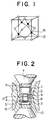
- Fig. 1 is a schematic view of the crystal structure of cBN single crystal.
- Fig. 2 is a cross-sectional view of an apparatus for the preparation of the composite material of the present invention, used in Examples 1 to 3.
- Fig. 3 is a Raman spectrum of cBN growth on a diamond substrate according to the present invention in Examples 1 to 3.
- Fig. 1 is a schematic view of the crystal structure of a cBN single crystal, in which N atoms are represented by ⁇ and B atoms are represented by o.
- cBN has a crystal structure of the zincblende type, similar to diamond.
- the lattice constants of diamond and cBN are respectively 3.567 ⁇ and 3.615 ⁇ , corresponding to a lattice mismatch of about 1.3%. Since their thermal expansion coefficients are also close, i.e. respectively 4.50x10 ⁇ 6 K ⁇ 1 (700°C) and 4.30x10 ⁇ 6 K ⁇ 1 (750°C), it is not impossible to grow cBN on a diamond substrate, but actually, this has not been realised. That is, cBN crystal could not be grown on a diamond substrate in the prior art under such a condition that the diamond substrate was stable.
- the cBN grown on a diamond substrate with an electric insulation according to the present invention is single crystal cBN.
- this cBN is doped with an additional element as an impurity, a semiconductor cBN with a diamond substrate can be obtained.
- a semiconductor cBN grown on an insulating substrate can be provided and making the best use of the property peculiar to cBN, i.e. its wide band gap, a semiconductor device capable of operating at a high temperature and a semiconductor optical device capable of emitting ultraviolet rays can be realized.
- the composite material of the present invention consists of cBN and a diamond substrate, which can be applied to a diode capable of operating at a high temperature, i.e. 500 to 600°C,or a semiconductor optical device capable of emitting ultraviolet rays by the best use of the excellent properties peculiar to cBN as a semiconductor, for example, wide band gap and thermal and chemical stability.
- the composite material of the present invention was produced by growing cBN on a diamond substrate.
- a reaction chamber was surrounded by a molybdenum capsule 3 to prevent it from direct contact with a pressure medium 2 such as hBN and heated at a predetermined temperature by passing AC or DC current through a graphite heater 1.
- a boron nitride source 4 was arranged so as to be at a higher temperature than a diamond substrate 5 and a solvent 6 such as Li3SrBN2 was arranged between the boron nitride source 4 and diamond substrate 5.
- boron nitride was dissolved in the solvent 6 from the boron nitride source 4 at a high temperature and high pressure at which cBN was stable and precipitated on the substrate crystal 5 at the relatively lower temperature, based on the solubility difference of boron nitride due to the temperature difference.
- Fig. 2 7 designates an anvil, 8 designates a die, 9 designates a heat insulating pressure medium and 10 designates a power supply part.
- ⁇ T means a temperature gradient between the boron nitride source 4 and diamond substrate 5.
- the pretreatment for the removal of oxygen was carried out by heating and calcining the boron nitride source for 1 to 2 hours in high purity nitrogen at 2000 to 2100°C to reduce the oxygen content to 10 ppm or less.
- the substrate crystal 5 there was used a diamond single crystal of artificial Ib type with a maximum side of 3 mm, which was arranged in such a manner that its (1 1 1) plane was contacted with the solvent 6.
- cBN was grown under the similar conditions to Example 1 but using artificial diamond of IIa type as a substrate instead of the artificial diamond of Ib type used in Example 1 and the boron nitride source further containing 4% by weight of Be powder.
- the thus resulting film was a blue film with a thickness of about 100 ⁇ m, having an electric resistance of about 103 ⁇ cm and being electrically conductive.
- cBN was grown under the similar conditions to Example 1 but using the boron nitride source 4 of Example 2, to which 5% by weight of silicon powder was further added.
- the thus resulting film was an orange film with a thickness of about 80 ⁇ m, having an electric resistance of about 104 ⁇ cm and being electrically conductive.
- a cBN film was grown by a vapor phase method wherein B2H6, N2 and H2 as raw material gases were fed to a reaction chamber respectively at flow rates of 10 cc/min, 10 cc/min and 100 cc/min and while adjusting the pressure inside the reaction chamber to 1 torr, and these gases were reacted for 4 hours at a DC plasma discharge output of 500 W, substrate temperature of 600°C and tungsten filament temperature of 200°C for preheating, and consequently, a film with a thickness of about 10 ⁇ m was deposited on the substrate surface.
- the raw material gas had an oxygen content corresponding to 1.33 x 10 ⁇ 7 Pascal.l/sec (10 ⁇ 9 torr.l/sec). Identification of the thus resulting film by a Raman spectrum told that it consisted of cBN having sharp peaks near 1304 cm ⁇ 1 and 1055 cm ⁇ 1.
Landscapes
- Chemical & Material Sciences (AREA)
- Organic Chemistry (AREA)
- Engineering & Computer Science (AREA)
- Crystallography & Structural Chemistry (AREA)
- Materials Engineering (AREA)
- Metallurgy (AREA)
- Chemical Kinetics & Catalysis (AREA)
- Inorganic Chemistry (AREA)
- Crystals, And After-Treatments Of Crystals (AREA)
- Carbon And Carbon Compounds (AREA)
- Semiconductor Lasers (AREA)
- Glass Compositions (AREA)
Description
- This invention relates to a composite material consisting of an insulating substrate of single crystal diamond and cubic boron nitride epitaxially grown thereon.
- It is generally known that cubic boron nitride (hereinafter referred to as "cBN") has the largest band gap (6 to 7 eV) as a semiconductor material and both P type and N type semiconductor can be prepared therefrom by the addition of impurities. Thus, it has eagerly been desired to develop the cBN semiconductors for the devices operated at high temperature or ultraviolet semiconductor laser device.
- When a crystal is grown, in general, the growth is carried out on a substrate and as a substrate for the growth of a cBN single crystal, there has hitherto been used only cBN itself. However, cBN having such a size and quality as to be suitable for use as a substrate has not been obtained up to the present time. Therefore, a good single crystal substrate as a substitute for cBN itself is essential considering the above described application and development of cBN as a semiconductor material.
- As a substrate material for the growth of cBN, diamond having a lattice mismatch with cBN of only about 1.3% and a substantially equal thermal expansion coefficient has been taken into consideration and up to the present time, a hetero junction of diamond and cBN has been proposed, for example, by W.E. Picket, Phys. Rev. B. vol. 38, 1316, 1988.
- However, no report has been made on the growth of cBN on diamond as a substrate. There has been no such precedent as succeeding in the growth of cBN on the heterogeneous substrate. That is, when considering the application of cBN to semiconductor devices operated at high temperatures, semiconductor optical devices capable of emitting ultraviolet rays, etc., which have hitherto not been prepared, there arises a problem that there is no suitable substrate for the growth of cBN.
- We have now developed a composite material comprising cBN formed on a diamond substrate, the composite maerial containing a P type or N type semiconductor of cBN single crystal.
- We have made various studies and experiments for the growth of cBN using diamond considered most suitable as a substrate material for cBN so as to solve the above described problems and consequently, have found surprisingly that diamond can stably exist even under the cBN-forming conditions by reducing the oxygen content from the atmosphere in which cBN is formed on a diamond substrate. Based on this finding, we have reached the composite material comprising cBN formed on diamond.
- Accordingly, the present invention provides a composite material comprising a single crystal diamond having electric insulation and single crystal cBN formed on one surface of the single crystal diamond as a substrate in such a manner that the single crystal cBN has the same plane index on the substrate wherein the single crystal cBN is a semiconductor of the P type which is doped with Be as an impurity or a semiconductor of the N type which is doped with at least one of Si, S, Ge or Se. In general, the cBN layer has a thickness of 10 to 100 µm and the diamond substrate has a thickness of 1 to 5 mm.
- In particularly preferred embodiments of the present invention, the above described composite materials can be provided in which the single crystal diamond substrate is of an artificial Ib type diamond single crystal or wherein the single crystal diamond substrate is of an artificial IIa type diamond single crystal.
- In the composite material of the present invention, the diamond as a substrate for the growth of cBN is electrically insulating and has a resistivity of at least 10⁴ Ωcm (25°C). Such diamond includes, for example, natural or artificial diamonds of the Ia type, Ib type and IIa type, each having an electric resistivity of 10⁴ to 10¹⁶ Ωnm (25°C). Almost all natural diamonds are of the Ia type, and diamonds synthesized artificially at an ultra-high pressure are usually of the Ib type, but diamond of the IIa type can be synthesized at an ultra-high pressure by adding a material which is a nitrogen lover to the catalyst. In the present invention, therefore, artificial diamonds of the Ib type and IIa type are particularly preferred as the substrate.
- The P type semiconductor is obtained by doping the grown cBN layer with Be as an impurity and the N type semiconductor is obtained by doping the cBN layer with Si, S, Ge or Se.
- The composite material of the present invention can be prepared by reducing the oxygen content from the atmosphere in which the cBN is formed on a diamond substrate by a high temperature and high pressure method, or by a CVD method. Preferably, hexagonal boron nitride (hereinafter referred to as "hBN") as a raw material and a solvent material are used which are purified to a high purity and which have a very small oxygen content, or hBN and a solvent material are used each or both of which contain a low oxygen formation energy material such as Mg, Al, Ca, V, Ti, Zr and the like.
- In the conventional high temperature and high pressure method, the raw material usually conatins 100 to 200 ppm of oxygen and in the conventional CVD method, the raw material gas usually contains 1.33 x 10⁻⁵ to 10⁻⁴ Pascal.ℓ/sec (10⁻⁷ to 10 ⁻⁶, torr.ℓ/sec). In the present invention, on the contrary, the oxygen contents are generally reduced to 5 to 10 ppm and 1.33 x 10⁻⁶ to 10⁻⁷ Pascal.ℓ/sec (10⁻⁸ to 10⁻⁹ torr.ℓ/sec), respectively.
- The accompanying drawings are to illustrate in detail the principle and merits of the present invention.
- Fig. 1 is a schematic view of the crystal structure of cBN single crystal.
- Fig. 2 is a cross-sectional view of an apparatus for the preparation of the composite material of the present invention, used in Examples 1 to 3.
- Fig. 3 is a Raman spectrum of cBN growth on a diamond substrate according to the present invention in Examples 1 to 3.
- Fig. 1 is a schematic view of the crystal structure of a cBN single crystal, in which N atoms are represented by ● and B atoms are represented by o. As can be seen from this figure, cBN has a crystal structure of the zincblende type, similar to diamond. The lattice constants of diamond and cBN are respectively 3.567 Å and 3.615 Å, corresponding to a lattice mismatch of about 1.3%. Since their thermal expansion coefficients are also close, i.e. respectively 4.50x10⁻⁶ K⁻¹ (700°C) and 4.30x10⁻⁶ K⁻¹ (750°C), it is not impossible to grow cBN on a diamond substrate, but actually, this has not been realised. That is, cBN crystal could not be grown on a diamond substrate in the prior art under such a condition that the diamond substrate was stable.
- We have made various studies to find the reason that the diamond substrate cannot stably be present and consequently, have found that this is due to the reaction of the diamond with oxygen in the atmosphere for the growth of cBN. Based on this finding, it can be confirmed that cBN can readily be grown on a diamond substrate if oxygen is completely removed from the atmosphere or reduced to the oxygen content hereinbefore described for the growth of cBN and the present invention is thus realized.
- It is found by the reflection high energy electron ray diffraction (RHEED) or Raman spectrum that the cBN grown on a diamond substrate with an electric insulation according to the present invention is single crystal cBN. When this cBN is doped with an additional element as an impurity, a semiconductor cBN with a diamond substrate can be obtained.
- As illustrated above, according to the present invention, a semiconductor cBN grown on an insulating substrate can be provided and making the best use of the property peculiar to cBN, i.e. its wide band gap, a semiconductor device capable of operating at a high temperature and a semiconductor optical device capable of emitting ultraviolet rays can be realized.
- The composite material of the present invention consists of cBN and a diamond substrate, which can be applied to a diode capable of operating at a high temperature, i.e. 500 to 600°C,or a semiconductor optical device capable of emitting ultraviolet rays by the best use of the excellent properties peculiar to cBN as a semiconductor, for example, wide band gap and thermal and chemical stability.
- Furthermore, since in the composite material of the present invention, diamond having electric insulation is used as a substrate, there is no electric interaction between the elements in an integrated circuit and high integration thereof is thus rendered easy, whereby very large scale integration can be realized by the joint use of the thermal property of the cBN semiconductor.
- The following examples are given in order to illustrate the present invention in detail without limiting the same.
- Using a high temperature and pressure generating apparatus as shown in Fig. 2, the composite material of the present invention was produced by growing cBN on a diamond substrate. In this apparatus, a reaction chamber was surrounded by a molybdenum capsule 3 to prevent it from direct contact with a
pressure medium 2 such as hBN and heated at a predetermined temperature by passing AC or DC current through agraphite heater 1. In the reaction chamber, a boron nitride source 4 was arranged so as to be at a higher temperature than a diamond substrate 5 and a solvent 6 such as Li₃SrBN₂ was arranged between the boron nitride source 4 and diamond substrate 5. The boron nitride was dissolved in the solvent 6 from the boron nitride source 4 at a high temperature and high pressure at which cBN was stable and precipitated on the substrate crystal 5 at the relatively lower temperature, based on the solubility difference of boron nitride due to the temperature difference. In Fig. 2, 7 designates an anvil, 8 designates a die, 9 designates a heat insulating pressure medium and 10 designates a power supply part. - ΔT means a temperature gradient between the boron nitride source 4 and diamond substrate 5.
- The specific data of this experiment were as follows:
As the boron nitride source 4, there was used a compact of 4 mm in diameter and 2 mm in height, consisting of powdered hBN and cBN which had been subjected to a pretreatment for completely removing oxygen, and as the solvent 6, there was used a compact of 4 mm in diameter and 7 mm in height, consisting of Li₃BrBN₂. - The pretreatment for the removal of oxygen was carried out by heating and calcining the boron nitride source for 1 to 2 hours in high purity nitrogen at 2000 to 2100°C to reduce the oxygen content to 10 ppm or less. As the substrate crystal 5, there was used a diamond single crystal of artificial Ib type with a maximum side of 3 mm, which was arranged in such a manner that its (1 1 1) plane was contacted with the solvent 6.
- When growth of cBN was carried out at a pressure of 65 kbar and a temperature of 1700°C for a retention time of 2 hours using the above described reaction system, a yellow film with a thickness of about 100 µm was formed on the diamond substrate. Identification of this film by a Raman spectrum told that it consisted of cBN crystal having a peak near 1304 cm⁻¹ and 1055 cm⁻¹ as shown in Fig. 3.
- cBN was grown under the similar conditions to Example 1 but using artificial diamond of IIa type as a substrate instead of the artificial diamond of Ib type used in Example 1 and the boron nitride source further containing 4% by weight of Be powder. The thus resulting film was a blue film with a thickness of about 100 µm, having an electric resistance of about 10³ Ωcm and being electrically conductive.
- cBN was grown under the similar conditions to Example 1 but using the boron nitride source 4 of Example 2, to which 5% by weight of silicon powder was further added. The thus resulting film was an orange film with a thickness of about 80 µm, having an electric resistance of about 10⁴ Ωcm and being electrically conductive.
- Using the (1 1 1) plane of an artificial diamond single crystal as a substrate, a cBN film was grown by a vapor phase method wherein B₂H₆, N₂ and H₂ as raw material gases were fed to a reaction chamber respectively at flow rates of 10 cc/min, 10 cc/min and 100 cc/min and while adjusting the pressure inside the reaction chamber to 1 torr, and these gases were reacted for 4 hours at a DC plasma discharge output of 500 W, substrate temperature of 600°C and tungsten filament temperature of 200°C for preheating, and consequently, a film with a thickness of about 10 µm was deposited on the substrate surface. The raw material gas had an oxygen content corresponding to 1.33 x 10⁻⁷ Pascal.ℓ/sec (10⁻⁹ torr.ℓ/sec). Identification of the thus resulting film by a Raman spectrum told that it consisted of cBN having sharp peaks near 1304 cm⁻¹ and 1055 cm⁻¹.
Claims (7)
- A composite material comprising a single crystal diamond having electric insulation and single crystal cBN formed on one surface of the single crystal diamond as a substrate in such a manner that the single crystal cBN has the same plane index on the substrate wherein the single crystal cBN is either a semiconductor of the P type which is doped with Be as an impurity or a semiconductor of the N type which is doped with at least one of Si, S, Ge or Se.
- A composite material as claimed in claim 1, wherein the single crystal diamond is that of the artificial Ib type.
- A composite material as claimed in claim 1, wherein the single crystal diamond is that of the artificial IIa type.
- A process for the production of the composite material as claimed in claim 1 by a high temperature and high pressure method, characterized in that an atmosphere in which cBN is formed on a diamond substrate has an oxygen concentration of 10 ppm or less.
- A process as claimed in claim 4, wherein hBN and a solvent material, used as raw materials, are purified to decrease the oxygen content thereof.
- A process as claimed in claim 4, wherein hBN and a solvent material, used as raw materials, contain at least one of Mg, Al, Ca, V, Ti and Zr.
- A process for the production of the composite material as claimed in claim 1 by the CVD method, characterized in that an atmosphere in which cBN is formed on a diamond substrate has an oxygen partial pressure of 1.33 x 10⁻⁶ to 10⁻⁷ Pascal.ℓ/sec (10⁻⁸ to 10⁻⁹ torr.ℓ/sec).
Applications Claiming Priority (2)
| Application Number | Priority Date | Filing Date | Title |
|---|---|---|---|
| JP1009835A JPH02192494A (en) | 1989-01-20 | 1989-01-20 | Composite material |
| JP9835/89 | 1989-01-20 |
Publications (3)
| Publication Number | Publication Date |
|---|---|
| EP0379359A2 EP0379359A2 (en) | 1990-07-25 |
| EP0379359A3 EP0379359A3 (en) | 1990-12-19 |
| EP0379359B1 true EP0379359B1 (en) | 1994-08-03 |
Family
ID=11731185
Family Applications (1)
| Application Number | Title | Priority Date | Filing Date |
|---|---|---|---|
| EP90300506A Expired - Lifetime EP0379359B1 (en) | 1989-01-20 | 1990-01-18 | A composite material |
Country Status (5)
| Country | Link |
|---|---|
| US (1) | US5043219A (en) |
| EP (1) | EP0379359B1 (en) |
| JP (1) | JPH02192494A (en) |
| DE (1) | DE69011142T2 (en) |
| ES (1) | ES2060010T3 (en) |
Families Citing this family (11)
| Publication number | Priority date | Publication date | Assignee | Title |
|---|---|---|---|---|
| EP0420188A1 (en) * | 1989-09-27 | 1991-04-03 | Sumitomo Electric Industries, Ltd. | Semiconductor heterojunction structure |
| JP3104979B2 (en) * | 1990-07-27 | 2000-10-30 | 株式会社東芝 | Ultraviolet semiconductor laser, semiconductor device, and manufacturing method thereof |
| EP0562549B1 (en) * | 1992-03-24 | 1998-07-01 | Sumitomo Electric Industries, Ltd. | Heterojunction bipolar transistor containing silicon carbide |
| US5597625A (en) * | 1993-02-10 | 1997-01-28 | California Institute Of Technology | Low pressure growth of cubic boron nitride films |
| KR0142150B1 (en) * | 1993-04-09 | 1998-07-15 | 윌리엄 티. 엘리스 | Method for Etching Boron Nitride |
| JPH07161455A (en) * | 1993-12-09 | 1995-06-23 | Sumitomo Electric Ind Ltd | Diamond heater |
| US5620754A (en) * | 1994-01-21 | 1997-04-15 | Qqc, Inc. | Method of treating and coating substrates |
| US5554415A (en) * | 1994-01-18 | 1996-09-10 | Qqc, Inc. | Substrate coating techniques, including fabricating materials on a surface of a substrate |
| US5731046A (en) * | 1994-01-18 | 1998-03-24 | Qqc, Inc. | Fabrication of diamond and diamond-like carbon coatings |
| DE4415600A1 (en) * | 1994-05-04 | 1995-11-30 | Daimler Benz Ag | Electronic component with a semiconductor composite structure |
| WO2018185909A1 (en) * | 2017-04-06 | 2018-10-11 | 龍司 大島 | Monocrystalline diamond particles containing cubic crystalline boron nitride particles and production method therefor |
Family Cites Families (15)
| Publication number | Priority date | Publication date | Assignee | Title |
|---|---|---|---|---|
| US4143544A (en) * | 1977-06-22 | 1979-03-13 | General Electric Company | Fingerprinting crystals |
| JPH06105779B2 (en) * | 1983-02-28 | 1994-12-21 | 双葉電子工業株式会社 | Semiconductor device and manufacturing method thereof |
| SE453474B (en) * | 1984-06-27 | 1988-02-08 | Santrade Ltd | COMPOUND BODY COATED WITH LAYERS OF POLYCristalline DIAMANT |
| US4551195A (en) * | 1984-09-25 | 1985-11-05 | Showa Denko Kabushiki Kaisha | Method for growing boron nitride crystals of cubic system |
| JPS61106494A (en) * | 1984-10-29 | 1986-05-24 | Kyocera Corp | Member coated with diamond and its production |
| EP0220462B1 (en) * | 1985-09-24 | 1990-09-19 | Sumitomo Electric Industries, Ltd. | Method of synthesizing cubic system boron nitride |
| US4683043A (en) * | 1986-01-21 | 1987-07-28 | Battelle Development Corporation | Cubic boron nitride preparation |
| EP0255327B1 (en) * | 1986-07-30 | 1991-06-19 | De Beers Industrial Diamond Division (Proprietary) Limited | Cubic boron nitride manufacture |
| KR900008505B1 (en) * | 1987-02-24 | 1990-11-24 | 세미콘덕터 에너지 라보라터리 캄파니 리미티드 | Microwave Enhanced CVD Method for Carbon Precipitation |
| US4875967A (en) * | 1987-05-01 | 1989-10-24 | National Institute For Research In Inorganic Materials | Method for growing a single crystal of cubic boron nitride semiconductor and method for forming a p-n junction thereof, and light emitting element |
| US4816291A (en) * | 1987-08-19 | 1989-03-28 | The Regents Of The University Of California | Process for making diamond, doped diamond, diamond-cubic boron nitride composite films |
| JPH01236687A (en) * | 1988-03-17 | 1989-09-21 | Matsushita Electric Ind Co Ltd | Manufacturing method for through-hole printed circuit board |
| JPH0277454A (en) * | 1988-06-22 | 1990-03-16 | Mitsui Petrochem Ind Ltd | Molecule orientated molded article of ultra-high-molecular-weight polyolefin base resin |
| US5006914A (en) * | 1988-12-02 | 1991-04-09 | Advanced Technology Materials, Inc. | Single crystal semiconductor substrate articles and semiconductor devices comprising same |
| US4961958A (en) * | 1989-06-30 | 1990-10-09 | The Regents Of The Univ. Of Calif. | Process for making diamond, and doped diamond films at low temperature |
-
1989
- 1989-01-20 JP JP1009835A patent/JPH02192494A/en active Pending
-
1990
- 1990-01-18 ES ES90300506T patent/ES2060010T3/en not_active Expired - Lifetime
- 1990-01-18 DE DE69011142T patent/DE69011142T2/en not_active Expired - Fee Related
- 1990-01-18 EP EP90300506A patent/EP0379359B1/en not_active Expired - Lifetime
- 1990-01-19 US US07/467,542 patent/US5043219A/en not_active Expired - Fee Related
Also Published As
| Publication number | Publication date |
|---|---|
| EP0379359A2 (en) | 1990-07-25 |
| US5043219A (en) | 1991-08-27 |
| JPH02192494A (en) | 1990-07-30 |
| DE69011142D1 (en) | 1994-09-08 |
| EP0379359A3 (en) | 1990-12-19 |
| DE69011142T2 (en) | 1994-12-08 |
| ES2060010T3 (en) | 1994-11-16 |
Similar Documents
| Publication | Publication Date | Title |
|---|---|---|
| EP0282075B1 (en) | Thin film single crystal substrate | |
| EP0442304B1 (en) | Polycrystalline CVD diamond substrate for single crystal epitaxial growth of semiconductors | |
| EP0282054B1 (en) | Thin film single crystal diamond substrate | |
| JP3876473B2 (en) | Nitride single crystal and manufacturing method thereof | |
| US5494753A (en) | Articles having thermal conductors of graphite | |
| JP2730145B2 (en) | Method of forming single crystal diamond layer | |
| JPH08236445A (en) | Single crystal semiconductor on substrate and manufacturing method thereof | |
| EP0526468A1 (en) | Diamond-on-a-substrate for electronic applications | |
| EP0389533A1 (en) | SUBLIMATION GROWTH OF SILICON CARBIDE SINGLE CRYSTALS. | |
| US5043219A (en) | Composite material | |
| US4865659A (en) | Heteroepitaxial growth of SiC on Si | |
| EP0386727A1 (en) | Method for producing single crystal diamond film | |
| JP3666044B2 (en) | Diamond parts | |
| KR102611922B1 (en) | Apparatus and method for manufacturing hexagonal Si crystal | |
| JP3728464B2 (en) | Method for manufacturing substrate for vapor phase synthesis of single crystal diamond film | |
| WO1997013891A1 (en) | METHOD OF MANUFACTURING EPITAXIAL LAYERS OF GaN OR Ga(A1,In)N ON SINGLE CRYSTAL GaN AND MIXED Ga(A1,In)N SUBSTRATES | |
| JPH06107494A (en) | Vapor growth method of diamond | |
| v. Münch | Silicon carbide technology for blue-emitting diodes | |
| JP2620293B2 (en) | Diamond modification method | |
| JPH0666273B2 (en) | Thin film single crystal diamond substrate | |
| JPH02199098A (en) | Production of single crystal diamond | |
| JP3728555B2 (en) | Single crystal diamond film substrate | |
| JPH05102048A (en) | Diamond substrate and manufacturing method thereof | |
| JPH05102047A (en) | Diamond substrate and manufacturing method thereof | |
| Chu et al. | Gallium nitride optoelectronic devices |
Legal Events
| Date | Code | Title | Description |
|---|---|---|---|
| PUAI | Public reference made under article 153(3) epc to a published international application that has entered the european phase |
Free format text: ORIGINAL CODE: 0009012 |
|
| AK | Designated contracting states |
Kind code of ref document: A2 Designated state(s): DE ES FR GB GR SE |
|
| PUAL | Search report despatched |
Free format text: ORIGINAL CODE: 0009013 |
|
| AK | Designated contracting states |
Kind code of ref document: A3 Designated state(s): DE ES FR GB GR SE |
|
| 17P | Request for examination filed |
Effective date: 19910527 |
|
| 17Q | First examination report despatched |
Effective date: 19930216 |
|
| GRAA | (expected) grant |
Free format text: ORIGINAL CODE: 0009210 |
|
| AK | Designated contracting states |
Kind code of ref document: B1 Designated state(s): DE ES FR GB GR SE |
|
| REF | Corresponds to: |
Ref document number: 69011142 Country of ref document: DE Date of ref document: 19940908 |
|
| ET | Fr: translation filed | ||
| REG | Reference to a national code |
Ref country code: ES Ref legal event code: FG2A Ref document number: 2060010 Country of ref document: ES Kind code of ref document: T3 |
|
| REG | Reference to a national code |
Ref country code: GR Ref legal event code: FG4A Free format text: 3013707 |
|
| EAL | Se: european patent in force in sweden |
Ref document number: 90300506.4 |
|
| PLBE | No opposition filed within time limit |
Free format text: ORIGINAL CODE: 0009261 |
|
| STAA | Information on the status of an ep patent application or granted ep patent |
Free format text: STATUS: NO OPPOSITION FILED WITHIN TIME LIMIT |
|
| 26N | No opposition filed | ||
| PGFP | Annual fee paid to national office [announced via postgrant information from national office to epo] |
Ref country code: GR Payment date: 19951229 Year of fee payment: 7 |
|
| PGFP | Annual fee paid to national office [announced via postgrant information from national office to epo] |
Ref country code: GB Payment date: 19960109 Year of fee payment: 7 Ref country code: FR Payment date: 19960109 Year of fee payment: 7 |
|
| PGFP | Annual fee paid to national office [announced via postgrant information from national office to epo] |
Ref country code: SE Payment date: 19960119 Year of fee payment: 7 |
|
| PGFP | Annual fee paid to national office [announced via postgrant information from national office to epo] |
Ref country code: ES Payment date: 19960126 Year of fee payment: 7 Ref country code: DE Payment date: 19960126 Year of fee payment: 7 |
|
| PG25 | Lapsed in a contracting state [announced via postgrant information from national office to epo] |
Ref country code: GB Effective date: 19970118 |
|
| PG25 | Lapsed in a contracting state [announced via postgrant information from national office to epo] |
Ref country code: SE Effective date: 19970119 |
|
| PG25 | Lapsed in a contracting state [announced via postgrant information from national office to epo] |
Ref country code: ES Free format text: LAPSE BECAUSE OF NON-PAYMENT OF DUE FEES Effective date: 19970120 |
|
| PG25 | Lapsed in a contracting state [announced via postgrant information from national office to epo] |
Ref country code: GR Free format text: THE PATENT HAS BEEN ANNULLED BY A DECISION OF A NATIONAL AUTHORITY Effective date: 19970731 |
|
| REG | Reference to a national code |
Ref country code: GR Ref legal event code: MM2A Free format text: 3013707 |
|
| GBPC | Gb: european patent ceased through non-payment of renewal fee |
Effective date: 19970118 |
|
| PG25 | Lapsed in a contracting state [announced via postgrant information from national office to epo] |
Ref country code: FR Effective date: 19970930 |
|
| PG25 | Lapsed in a contracting state [announced via postgrant information from national office to epo] |
Ref country code: DE Effective date: 19971001 |
|
| EUG | Se: european patent has lapsed |
Ref document number: 90300506.4 |
|
| REG | Reference to a national code |
Ref country code: FR Ref legal event code: ST |
|
| REG | Reference to a national code |
Ref country code: ES Ref legal event code: FD2A Effective date: 19990301 |