EP0369352B2 - Capacitance type accelerometer and method of manufacturing the same - Google Patents
Capacitance type accelerometer and method of manufacturing the same Download PDFInfo
- Publication number
- EP0369352B2 EP0369352B2 EP89120880A EP89120880A EP0369352B2 EP 0369352 B2 EP0369352 B2 EP 0369352B2 EP 89120880 A EP89120880 A EP 89120880A EP 89120880 A EP89120880 A EP 89120880A EP 0369352 B2 EP0369352 B2 EP 0369352B2
- Authority
- EP
- European Patent Office
- Prior art keywords
- silicon
- movable electrode
- electrode part
- plates
- capacitance type
- Prior art date
- Legal status (The legal status is an assumption and is not a legal conclusion. Google has not performed a legal analysis and makes no representation as to the accuracy of the status listed.)
- Expired - Lifetime
Links
- 238000004519 manufacturing process Methods 0.000 title claims description 11
- XUIMIQQOPSSXEZ-UHFFFAOYSA-N Silicon Chemical compound [Si] XUIMIQQOPSSXEZ-UHFFFAOYSA-N 0.000 claims description 96
- 229910052710 silicon Inorganic materials 0.000 claims description 96
- 239000010703 silicon Substances 0.000 claims description 96
- 230000001133 acceleration Effects 0.000 claims description 18
- 238000000926 separation method Methods 0.000 claims 2
- 238000001514 detection method Methods 0.000 description 17
- 238000000034 method Methods 0.000 description 17
- 230000003647 oxidation Effects 0.000 description 12
- 238000007254 oxidation reaction Methods 0.000 description 12
- 239000011521 glass Substances 0.000 description 7
- 238000010438 heat treatment Methods 0.000 description 7
- 238000012545 processing Methods 0.000 description 7
- 230000035945 sensitivity Effects 0.000 description 5
- 238000005530 etching Methods 0.000 description 4
- 238000010276 construction Methods 0.000 description 3
- 239000007789 gas Substances 0.000 description 3
- 239000004020 conductor Substances 0.000 description 2
- 238000009792 diffusion process Methods 0.000 description 2
- 230000002349 favourable effect Effects 0.000 description 2
- BASFCYQUMIYNBI-UHFFFAOYSA-N platinum Chemical compound [Pt] BASFCYQUMIYNBI-UHFFFAOYSA-N 0.000 description 2
- 239000004065 semiconductor Substances 0.000 description 2
- RZVAJINKPMORJF-UHFFFAOYSA-N Acetaminophen Chemical compound CC(=O)NC1=CC=C(O)C=C1 RZVAJINKPMORJF-UHFFFAOYSA-N 0.000 description 1
- SGPGESCZOCHFCL-UHFFFAOYSA-N Tilisolol hydrochloride Chemical compound [Cl-].C1=CC=C2C(=O)N(C)C=C(OCC(O)C[NH2+]C(C)(C)C)C2=C1 SGPGESCZOCHFCL-UHFFFAOYSA-N 0.000 description 1
- QVGXLLKOCUKJST-UHFFFAOYSA-N atomic oxygen Chemical compound [O] QVGXLLKOCUKJST-UHFFFAOYSA-N 0.000 description 1
- 239000003990 capacitor Substances 0.000 description 1
- 239000004567 concrete Substances 0.000 description 1
- 238000007796 conventional method Methods 0.000 description 1
- 230000001419 dependent effect Effects 0.000 description 1
- 230000006866 deterioration Effects 0.000 description 1
- 230000002542 deteriorative effect Effects 0.000 description 1
- 238000010586 diagram Methods 0.000 description 1
- 239000000428 dust Substances 0.000 description 1
- 230000000694 effects Effects 0.000 description 1
- 230000008713 feedback mechanism Effects 0.000 description 1
- 230000005484 gravity Effects 0.000 description 1
- 239000011810 insulating material Substances 0.000 description 1
- 238000003475 lamination Methods 0.000 description 1
- 239000000463 material Substances 0.000 description 1
- 238000005259 measurement Methods 0.000 description 1
- 229910052751 metal Inorganic materials 0.000 description 1
- 239000002184 metal Substances 0.000 description 1
- 230000003287 optical effect Effects 0.000 description 1
- 229910052760 oxygen Inorganic materials 0.000 description 1
- 239000001301 oxygen Substances 0.000 description 1
- 238000004806 packaging method and process Methods 0.000 description 1
- 229910052697 platinum Inorganic materials 0.000 description 1
- 239000000843 powder Substances 0.000 description 1
- 238000007781 pre-processing Methods 0.000 description 1
- 239000005297 pyrex Substances 0.000 description 1
- 150000003376 silicon Chemical class 0.000 description 1
- 229910000679 solder Inorganic materials 0.000 description 1
- XLYOFNOQVPJJNP-UHFFFAOYSA-N water Substances O XLYOFNOQVPJJNP-UHFFFAOYSA-N 0.000 description 1
Images




Classifications
-
- B—PERFORMING OPERATIONS; TRANSPORTING
- B81—MICROSTRUCTURAL TECHNOLOGY
- B81C—PROCESSES OR APPARATUS SPECIALLY ADAPTED FOR THE MANUFACTURE OR TREATMENT OF MICROSTRUCTURAL DEVICES OR SYSTEMS
- B81C1/00—Manufacture or treatment of devices or systems in or on a substrate
- B81C1/00015—Manufacture or treatment of devices or systems in or on a substrate for manufacturing microsystems
- B81C1/00261—Processes for packaging MEMS devices
- B81C1/00301—Connecting electric signal lines from the MEMS device with external electrical signal lines, e.g. through vias
-
- G—PHYSICS
- G01—MEASURING; TESTING
- G01P—MEASURING LINEAR OR ANGULAR SPEED, ACCELERATION, DECELERATION, OR SHOCK; INDICATING PRESENCE, ABSENCE, OR DIRECTION, OF MOVEMENT
- G01P15/00—Measuring acceleration; Measuring deceleration; Measuring shock, i.e. sudden change of acceleration
- G01P15/02—Measuring acceleration; Measuring deceleration; Measuring shock, i.e. sudden change of acceleration by making use of inertia forces using solid seismic masses
- G01P15/08—Measuring acceleration; Measuring deceleration; Measuring shock, i.e. sudden change of acceleration by making use of inertia forces using solid seismic masses with conversion into electric or magnetic values
- G01P15/0802—Details
-
- G—PHYSICS
- G01—MEASURING; TESTING
- G01P—MEASURING LINEAR OR ANGULAR SPEED, ACCELERATION, DECELERATION, OR SHOCK; INDICATING PRESENCE, ABSENCE, OR DIRECTION, OF MOVEMENT
- G01P15/00—Measuring acceleration; Measuring deceleration; Measuring shock, i.e. sudden change of acceleration
- G01P15/02—Measuring acceleration; Measuring deceleration; Measuring shock, i.e. sudden change of acceleration by making use of inertia forces using solid seismic masses
- G01P15/08—Measuring acceleration; Measuring deceleration; Measuring shock, i.e. sudden change of acceleration by making use of inertia forces using solid seismic masses with conversion into electric or magnetic values
- G01P15/125—Measuring acceleration; Measuring deceleration; Measuring shock, i.e. sudden change of acceleration by making use of inertia forces using solid seismic masses with conversion into electric or magnetic values by capacitive pick-up
-
- G—PHYSICS
- G01—MEASURING; TESTING
- G01P—MEASURING LINEAR OR ANGULAR SPEED, ACCELERATION, DECELERATION, OR SHOCK; INDICATING PRESENCE, ABSENCE, OR DIRECTION, OF MOVEMENT
- G01P15/00—Measuring acceleration; Measuring deceleration; Measuring shock, i.e. sudden change of acceleration
- G01P15/02—Measuring acceleration; Measuring deceleration; Measuring shock, i.e. sudden change of acceleration by making use of inertia forces using solid seismic masses
- G01P15/08—Measuring acceleration; Measuring deceleration; Measuring shock, i.e. sudden change of acceleration by making use of inertia forces using solid seismic masses with conversion into electric or magnetic values
- G01P15/13—Measuring acceleration; Measuring deceleration; Measuring shock, i.e. sudden change of acceleration by making use of inertia forces using solid seismic masses with conversion into electric or magnetic values by measuring the force required to restore a proofmass subjected to inertial forces to a null position
- G01P15/131—Measuring acceleration; Measuring deceleration; Measuring shock, i.e. sudden change of acceleration by making use of inertia forces using solid seismic masses with conversion into electric or magnetic values by measuring the force required to restore a proofmass subjected to inertial forces to a null position with electrostatic counterbalancing means
-
- B—PERFORMING OPERATIONS; TRANSPORTING
- B81—MICROSTRUCTURAL TECHNOLOGY
- B81B—MICROSTRUCTURAL DEVICES OR SYSTEMS, e.g. MICROMECHANICAL DEVICES
- B81B2201/00—Specific applications of microelectromechanical systems
- B81B2201/02—Sensors
- B81B2201/0228—Inertial sensors
- B81B2201/0235—Accelerometers
-
- B—PERFORMING OPERATIONS; TRANSPORTING
- B81—MICROSTRUCTURAL TECHNOLOGY
- B81B—MICROSTRUCTURAL DEVICES OR SYSTEMS, e.g. MICROMECHANICAL DEVICES
- B81B2207/00—Microstructural systems or auxiliary parts thereof
- B81B2207/09—Packages
- B81B2207/091—Arrangements for connecting external electrical signals to mechanical structures inside the package
- B81B2207/094—Feed-through, via
- B81B2207/095—Feed-through, via through the lid
-
- B—PERFORMING OPERATIONS; TRANSPORTING
- B81—MICROSTRUCTURAL TECHNOLOGY
- B81B—MICROSTRUCTURAL DEVICES OR SYSTEMS, e.g. MICROMECHANICAL DEVICES
- B81B2207/00—Microstructural systems or auxiliary parts thereof
- B81B2207/09—Packages
- B81B2207/091—Arrangements for connecting external electrical signals to mechanical structures inside the package
- B81B2207/094—Feed-through, via
- B81B2207/096—Feed-through, via through the substrate
-
- G—PHYSICS
- G01—MEASURING; TESTING
- G01P—MEASURING LINEAR OR ANGULAR SPEED, ACCELERATION, DECELERATION, OR SHOCK; INDICATING PRESENCE, ABSENCE, OR DIRECTION, OF MOVEMENT
- G01P15/00—Measuring acceleration; Measuring deceleration; Measuring shock, i.e. sudden change of acceleration
- G01P15/02—Measuring acceleration; Measuring deceleration; Measuring shock, i.e. sudden change of acceleration by making use of inertia forces using solid seismic masses
- G01P15/08—Measuring acceleration; Measuring deceleration; Measuring shock, i.e. sudden change of acceleration by making use of inertia forces using solid seismic masses with conversion into electric or magnetic values
- G01P2015/0805—Measuring acceleration; Measuring deceleration; Measuring shock, i.e. sudden change of acceleration by making use of inertia forces using solid seismic masses with conversion into electric or magnetic values being provided with a particular type of spring-mass-system for defining the displacement of a seismic mass due to an external acceleration
- G01P2015/0822—Measuring acceleration; Measuring deceleration; Measuring shock, i.e. sudden change of acceleration by making use of inertia forces using solid seismic masses with conversion into electric or magnetic values being provided with a particular type of spring-mass-system for defining the displacement of a seismic mass due to an external acceleration for defining out-of-plane movement of the mass
- G01P2015/0825—Measuring acceleration; Measuring deceleration; Measuring shock, i.e. sudden change of acceleration by making use of inertia forces using solid seismic masses with conversion into electric or magnetic values being provided with a particular type of spring-mass-system for defining the displacement of a seismic mass due to an external acceleration for defining out-of-plane movement of the mass for one single degree of freedom of movement of the mass
- G01P2015/0828—Measuring acceleration; Measuring deceleration; Measuring shock, i.e. sudden change of acceleration by making use of inertia forces using solid seismic masses with conversion into electric or magnetic values being provided with a particular type of spring-mass-system for defining the displacement of a seismic mass due to an external acceleration for defining out-of-plane movement of the mass for one single degree of freedom of movement of the mass the mass being of the paddle type being suspended at one of its longitudinal ends
Definitions
- the present invention relates to a capacitance type accelerometer and a method of manufacturing the same using a semiconductor manufacturing process, this capacitance type accelerometer being suitable for body control or engine control of an automobile.
- Such accelerometer includes a piezoelectric sensor conventionally utilizing a piezoelectric effect of a piezoelectric material, an electromagnetic servo system one having an electromagnetic feedback mechanism, a magnetic one utilizing a differential transformer, an optical one utilizing a photo-interrupter, and a strain gauge system or a capacitance system one utilizing a fine processing technique of silicon.
- the capacitance type accelerometer utilizing the fine processing technique of silicon is considered the most favorable, which can detect acceleration of the low frequency at high accuracy and provide an inexpensive sensor.
- the largest problem for packaging the capacitance type accelerometer is the package of the lead for electrode. Therefore, several methods are known.
- a first example, as disclosed in U.S. Patent 4,483,194, is a method to fetch the lead for the movable electrode or the fixed electrode through a P+ diffusion region.
- the method has the problem in that etching is complicated and yield when bonded is poor, the P+ diffusion region becomes a large stray capacitance, and its voltage dependency is large, thereby deteriorating the dejection system.
- a second example is a method to fetch the lead from a gap at the bonding portion of the silicon plate and a glass base.
- the method when a detected chip is diced by a usual dicing saw after the silicon plate and glass base are bonded in the wafer state, water content or chips enters into a space around the electrode through the gap, thereby creating the problem in that the performance as the accelerometer is not obtainable.
- a third example as disclosed "Miniature Silicon capacitance absolute pressure sensor", Page 255 to 260, I Mech E, 1981, is a method to fetch the lead through a bore perforating a glass base. This example is applied to the pressure sensor, in which the problem is created in the poor lead connection atone bore end caused by variation in metallizing condition and the temperature characteristic deterioration caused by a large difference in coefficient of thermal expansion between the solder charged in the other bore end and the glass base.
- a fourth example, as shown in U.S. Patent 4,609,968, is a method of using a silicon plate to the fixed electrode to package the silicon plate itself as part of the lead.
- a silicon plate to be the fixed electrode is applied at the periphery thereof with glass powder and baked and then polished at the surface to be like a mirror.
- a movable electrode and a silicon plate having a beam for supporting the electrode are laminated and bonded with anodic-bonding.
- the anodic bonding is to apply high voltage at a high temperature to glass and silicon to be bonded, in which the movable electrode is displaced by an electrostatic force and contacts with the silicon plate of fixed electrode so as to be discharged, whereby both the members cannot be bonded.
- the above-mentioned conventional technique is not considered as to the electrode lead package method, thereby creating the problem in the productivity, detection accuracy or sensitivity.
- GB-A-2 158 945 discloses a silicon capacitive accelerometer having the features of the precharacterizing part of daim 1, having alternatively a notch between the layers through which the fixed electrode is contacted or insulating material, only exemplified by Pyrex glass, between the laminated layers, and having several more obligatory features.
- An object of the present invention is to provide a capacitance type accelerometer and a method of manufacturing the same so that the accelerometer is superior in productivity, high in performance, and inexpensive to produce.
- Fig. 1 is a diagrammatic cross-sectional view showing an embodiment of an accelerometer in the present invention.
- Fig. 2 is a diagrammatic view showing an embodiment of a manufacturing process of the accelerometer shown in Fig. 1.
- Figs. 3 and 4 are diagrammatic cross-sectional views showing another embodiments of the accelerometers in the present invention.
- Figs. 5, 6 and 7 are developed cross-sectional views of the accelerometer shown in Fig. 1.
- Figs. 8(A), 8(B) and 8(C) are developed plane views of the embodiment of the accelerometer shown in Fig.7.
- Fig. 9 is an elevation of an embodiment of the accelerometer shown in Figs. 8(A), 8(B) and 8(C).
- Figs. 10(A) and 10(B) are equivalent circuits of the accelerometer.
- Figs. 11(A) and 11(B) are illustrations of a positioning method for a silicon plate in the wafer state at the embodiment of the present invention.
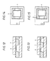
- Figs. 12, 13, 14 and 15 are developed plane views of the another embodiments of the accelerometer, Fig. 13 and 14 describing technological background.
- Fig 16 is a circuit diagram showing an embodiment of a signal processing circuit of an electro-static capacitance type accelerometer.
- Fig. 17 is a voltage wave form of a pulse width modulator.
- Fig. 18 is an output characteristic view of the accelerometer.
- FIG. 1 shows an embodiment of the present invention which concretes the manufacturing method.
- a detection unit of the embodiment of the capacitance type accelerometer comprises a silicon plate 1, a silicon plate 2 and a silicon plate 3, which are directly laminated and bonded through electrical insulating thermal oxidation films 4 and 5.
- a silicon beam 6 (a bridge-like portion) and a movable electrode 7 are preformed by etching prior to the bonding.
- the movable electrode 7 functioning as a weight is supported by the silicon beam 6, and gaps 8 between the movable electrode 7 and the silicon plates 1 and 3 change in dimension corresponding to the magnitude of acceleration vertical in the drawing and acting on the movable electrode 7.
- the silicon plates 1 and 3 opposite to the movable electrode 7 are the fixed electrodes.
- the capacity between the electrodes at the gap 8 varies corresponding to the acceleration acting on the detection unit, so that the acceleration is detected by use of the variation in the capacity.
- the movable electrode 7 is electrically connected with an external electronic circuit (not shown) through the silicon beam 6 and a bounding pad 9.
- the silicon plates 1 and 3 serve also as the fixed electrodes, they are usable as the lead-out terminals of the fixed electrodes, thereby extermely simplifying the lead package method.
- FIG. 2 A schematic manufacturing process of the detection unit shown in Fig. 1 is shown in Fig. 2, in which the silicon plates 1, 2 and 3 in the wafer state after finished of etching process and other pre-processings are fully cleaned to remove stain or dust from the bonding portion.
- the silicon plates in the wafer state are aligned and thereafter laminated, and subjected to heat treatment for 2 hours, at a temperature of 800°C, and in the oxygen atmosphere.
- the heat treatment can completely directly bond the silicon plates with each other through the thermal oxidation films.
- the three-layer bonded wafer of silicon is cut by the dicing saw, thereby enabling a large number of detection parts shown in Fig. 1 to be simultaneously manufactured.
- gas filled in the space around the movable electrode 7 and silicon beam 6 expands depending on a rate of heating up to the heat treatment temperature and the kind of atmospheric gas, whereby a gap is generated at part of laminated silicon plates 1, 2 and 3 to be bonded, whereby the bonding in the wafer state during the heat treatment may partially be improper.
- the Fig. 4 embodiment forms polycrystal silicon layers 11 and 12 at parts of silicon plates 1 and 3 opposite to the movable electrode 7.
- the polycrystal silicon layers 11 and 12 are of conductive material and substantially become fixed electrodes opposite to the movable electrode 7.
- the gaps between the movable electrode 7 and the polycrystal silicon layers 11 and 12 are reduced in width, thereby enabling an accelerometer of high sensitivity to be obtained. Also, since each gap can be of smaller width than thickness of each thermal oxidation film 4 or 5, the stray capacitance at parts of thermal oxidation films 4 and 5 is relative-reduced.
- the polycrystal silicon layers 11 and 12 fundamentally need only be conductor layers, which may be constructed of a metal layer, such as platinum.
- Figs. 5 through 7 are developed views of the construction of detection unit shown in the Fig. 1 embodiment before lamination.
- electrically insulating thermal oxidation films 4 and 5 are preformed only at the bonded portion between the silicon plates 1 and 3, and of at least 1 micron or more in thickness.
- the thermal oxidation films 4 and 5 are formed only at the bonding of silicon plate 2.
- the thermal oxidation films 4 and 5 are preformed at all the silicon plates 1, 2 and 3, which is more favorable than the embodiments in Figs. 5 and 6 in order to reduce the stray capacity at the parts after bonded.
- Figs. 8(A), 8(B) and 8(C) are developed plan views of the detection unit of the silicon capacitance type accelerometer of the present invention shown in Fig. 7 in which hatched portions show parts of thermal oxidation film as the bonding portion of silicon plates with each other.
- Reference numerals 9a, 9 and 9c designate bonding pads of the silicon plate 1 (functioning as the fixed electrode), movable electrode 7, and silicon plate 3 (functioning as the fixed electrode), the electrodes being connected with an external signal processing unit.
- Fig. 9 is an elevation view of the detection unit of the accelerometer of the invention, the detection unit being electrically connected with the external signal processing circuit through lead wires 15, 16 and 17.
- Fig. 10 shows an equivalent circuit of the detection unit.
- capacities 18 and 19 are capacities at the gap 8 between the electrodes, which change corresponding to magnitude of acceleration.
- capacities 20 and 21 are those by the thermal oxidation film at the silicon plate bonding portion, which are not at all affected by the acceleration. Therefore, the capacities 20 and 21 are made sufficiently smaller in magnitude than those 18 and 19, so that it is desirable to indicate the equivalent circuit substantially in Fig. 10(B). Therefore, it is effective to reduce an area of bounding, to make the thermal oxidation film larger in thickness, to enlarge the area of the movable electrode, and to reduce dimension of the gap between the electrodes.
- Fig. 11 (A) is a schematic view of a silicon plate 25 in the wafer state, in which reference numeral 23 designates detection chips, so that one wafercan produce several hundreds accelerometer, and, a plurality of through bores 22 are formed at the silicon plate 25 by etching.
- guide pins 24 are inserted into the through bores 22 so that the silicon plates 1, 2 and 3 are laminated and simultaneously positioned to each other.
- the positioning accuracy between the silicon plates depends on tolerance between each through bore 22 and the guide pin 24, thereby enabling positioning by accuracy of ⁇ several 10 microns or less.
- FIGs. 12 and 13 sectional views
- 14 and 15 plan views
- Fig. 12 shows an example in which a movable electrode 7 is held by a silicon beam 6 in a cantilever fashion, which is different from the Fig. 1 embodiment in that the silicon beam 6 is not disposed on the axis of gravity of movable electrode 7.
- the movable electrode 7 is supported by two silicon beams 6 in a both-ends support fashion.
- Figs. 14 and 15 show the detection units in which the movable electrode 7 is supported by four silicon beams 6 in the both-ends support fashion and by two silicon beams 6 in the cantilever fashion.
- Fig. 16 shows construction of the signal processing circuit.
- a detection unit shown in the drawing is essentially the same as that described in Fig. 1, in which the acceleration to be detected is defined by G, that in the direction of the arrow is defined to be positive, and that in the direction reverse to the arrow negative.
- Silicon plates 1,2 and 3 are connected to a ⁇ C detector 64 through conductive wires 15, 16 and 17.
- the ⁇ C detector 64 comprises switch and capacitors, and an amplifier 65 so controls a pulse width modulator 66 that a capacitance difference ⁇ C of the gaps 8 between the movable electrode 7 and the silicon plate 1 and 3 (serving also as the fixed electrode) becomes zero.
- Pulse-like output voltage V E is applied to the silicon plate 1 and output voltage -V E inverted by an inverter 67 to the silicon plate 3 in a feedback control manner.
- the silicon plate 2 is applied with constant DC voltage (In the drawing, 5 volts).
- a movable electrode 7 supported by a silicon beam 6 and functioning as a weight is intended to shift corresponding to magnitude of acceleration G.
- the position of movable electrode is controlled in a feedback manner by an electrostatic force acting between the electrodes. Therefore, electrostatic energy supplied between the electrodes leads to represent the acceleration G itself to be detected.
- the pulse-like output voltage waveform V E of pulse width modulator 66 is processed by a low-pass filter 68 and output voltage V O is fetched as the accelerometer through a differential amplifier 69.
- Fig. 17 shows the wave form of output voltage V E of the pulse width modulator.
- the output voltage V E is pulse-like voltage waveform of a cycle period of 50 ⁇ S, and its low level,is 0 volt, its high level 5 volts.
- the pulse width is controlled to linearly decrease with respect to the positive acceleration and increase to the negative acceleration.
- FIG. 18 An example of the output characteristic of the silicon capacitance type accelerometer is shown in Fig. 18, which result of measurement by the method shown in Fig. 16. As apparent from the above, acceleration of 0 to ⁇ 1G could be detected with good linearity and in high accuracy.
- the present invention can easily and reliably connect the detection unit and the exterior without creating any problem in package of the electrode lead, whereby the capacitance type accelerometer or the semiconductor pressure sensor superior in productivity, of high performance, and inexpensive to produce, can be provided with ease.
Landscapes
- Engineering & Computer Science (AREA)
- Physics & Mathematics (AREA)
- General Physics & Mathematics (AREA)
- Microelectronics & Electronic Packaging (AREA)
- Manufacturing & Machinery (AREA)
- Pressure Sensors (AREA)
- Measuring Fluid Pressure (AREA)
Description
- The present invention relates to a capacitance type accelerometer and a method of manufacturing the same using a semiconductor manufacturing process, this capacitance type accelerometer being suitable for body control or engine control of an automobile.
- It is required for an accelerometer for an automobile to detect acceleration of relative-low level (0 through ± 1.0 G) and the low frequency (0 to 10 Hz) at high accuracy. In addition, 1G = 9.8 m/S herein.
- Such accelerometer, as well-known, includes a piezoelectric sensor conventionally utilizing a piezoelectric effect of a piezoelectric material, an electromagnetic servo system one having an electromagnetic feedback mechanism, a magnetic one utilizing a differential transformer, an optical one utilizing a photo-interrupter, and a strain gauge system or a capacitance system one utilizing a fine processing technique of silicon. Among them the capacitance type accelerometer utilizing the fine processing technique of silicon is considered the most favorable, which can detect acceleration of the low frequency at high accuracy and provide an inexpensive sensor.
- The largest problem for packaging the capacitance type accelerometer is the package of the lead for electrode. Therefore, several methods are known.
- A first example, as disclosed in U.S. Patent 4,483,194, is a method to fetch the lead for the movable electrode or the fixed electrode through a P⁺ diffusion region. The method has the problem in that etching is complicated and yield when bonded is poor, the P⁺ diffusion region becomes a large stray capacitance, and its voltage dependency is large, thereby deteriorating the dejection system.
- A second example, as shown in Pages 336 to 339, Transducers '87 (the 4th International Conference on Solid-State Sensors and Actuators), is a method to fetch the lead from a gap at the bonding portion of the silicon plate and a glass base. The method, when a detected chip is diced by a usual dicing saw after the silicon plate and glass base are bonded in the wafer state, water content or chips enters into a space around the electrode through the gap, thereby creating the problem in that the performance as the accelerometer is not obtainable.
- A third example, as disclosed "Miniature Silicon capacitance absolute pressure sensor", Page 255 to 260, I Mech E, 1981, is a method to fetch the lead through a bore perforating a glass base. This example is applied to the pressure sensor, in which the problem is created in the poor lead connection atone bore end caused by variation in metallizing condition and the temperature characteristic deterioration caused by a large difference in coefficient of thermal expansion between the solder charged in the other bore end and the glass base.
- A fourth example, as shown in U.S. Patent 4,609,968, is a method of using a silicon plate to the fixed electrode to package the silicon plate itself as part of the lead. In this example, a silicon plate to be the fixed electrode is applied at the periphery thereof with glass powder and baked and then polished at the surface to be like a mirror. A movable electrode and a silicon plate having a beam for supporting the electrode are laminated and bonded with anodic-bonding. The anodic bonding is to apply high voltage at a high temperature to glass and silicon to be bonded, in which the movable electrode is displaced by an electrostatic force and contacts with the silicon plate of fixed electrode so as to be discharged, whereby both the members cannot be bonded. In order to avoid this, a gap between the movable electrode and the fixed electrode must be previously designed to be larger, or spring constant of the beam must be designed to be larger (in brief, deformation of the movable electrode with respect to the unit acceleration). As the result, the problem is created in that high sensitivity essentially possessed by the capacitance type accelerometer must largely be sacrificed.
- The above-mentioned conventional technique is not considered as to the electrode lead package method, thereby creating the problem in the productivity, detection accuracy or sensitivity.
- GB-A-2 158 945 discloses a silicon capacitive accelerometer having the features of the precharacterizing part of
daim 1, having alternatively a notch between the layers through which the fixed electrode is contacted or insulating material, only exemplified by Pyrex glass, between the laminated layers, and having several more obligatory features. - An object of the present invention is to provide a capacitance type accelerometer and a method of manufacturing the same so that the accelerometer is superior in productivity, high in performance, and inexpensive to produce.
- This object is accomplished with the features of the independent claims. Dependent claims are directed on preferred embodiments of the invention.
- Fig. 1 is a diagrammatic cross-sectional view showing an embodiment of an accelerometer in the present invention.
- Fig. 2 is a diagrammatic view showing an embodiment of a manufacturing process of the accelerometer shown in Fig. 1.
- Figs. 3 and 4 are diagrammatic cross-sectional views showing another embodiments of the accelerometers in the present invention.
- Figs. 5, 6 and 7 are developed cross-sectional views of the accelerometer shown in Fig. 1.
- Figs. 8(A), 8(B) and 8(C) are developed plane views of the embodiment of the accelerometer shown in Fig.7.
- Fig. 9 is an elevation of an embodiment of the accelerometer shown in Figs. 8(A), 8(B) and 8(C).
- Figs. 10(A) and 10(B) are equivalent circuits of the accelerometer.
- Figs. 11(A) and 11(B) are illustrations of a positioning method for a silicon plate in the wafer state at the embodiment of the present invention.
- Figs. 12, 13, 14 and 15 are developed plane views of the another embodiments of the accelerometer, Fig. 13 and 14 describing technological background.
- Fig 16 is a circuit diagram showing an embodiment of a signal processing circuit of an electro-static capacitance type accelerometer.
- Fig. 17 is a voltage wave form of a pulse width modulator.
- Fig. 18 is an output characteristic view of the accelerometer.
- Next, the accelerometer of the present invention will be detailed in accordance with an embodiment shown in the drawing.
- Fig. 1 shows an embodiment of the present invention which concretes the manufacturing method. A detection unit of the embodiment of the capacitance type accelerometer comprises a
silicon plate 1, asilicon plate 2 and asilicon plate 3, which are directly laminated and bonded through electrical insulatingthermal oxidation films silicon plate 2, a silicon beam 6 (a bridge-like portion) and amovable electrode 7 are preformed by etching prior to the bonding. Themovable electrode 7 functioning as a weight is supported by thesilicon beam 6, andgaps 8 between themovable electrode 7 and thesilicon plates movable electrode 7. Thesilicon plates movable electrode 7 are the fixed electrodes. The capacity between the electrodes at thegap 8 varies corresponding to the acceleration acting on the detection unit, so that the acceleration is detected by use of the variation in the capacity. - The
movable electrode 7 is electrically connected with an external electronic circuit (not shown) through thesilicon beam 6 and abounding pad 9. - As above-mentioned, since the
silicon plates - Meanwhile, in a case of this embodiment, electric capacity at the bonding portions (
parts silicon plate 2 and thesilicon plates gaps 8. The capacity of the bonding portion becomes stray capacitance not at all affected by variation in acceleration. Accordingly, the electric capacity at this part is desired to be as smaller as possible. For this purpose, an area of bonding portion need only be as small as possible, and on the other hand, thethermal oxidation films - A schematic manufacturing process of the detection unit shown in Fig. 1 is shown in Fig. 2, in which the
silicon plates - In this embodiment of the sensor which directly bonds the silicon plates only by the heat treatment, differently from the anodic-bonding method to apply high voltage, even when the size of
gap 8 or the spring constant ofsilicon beam 6 is reduced, any trouble is not generated during the manufacturing, thereby obtaining an accelerometer of high sensitivity with ease. - Other modified embodiments of the detection unit of the invention will be shown in Figs. 3 and 4. In addition, in the following drawings, the same reference numerals show the components of the same functions.
- When the silicon plates are directly bonded with each other by the method shown in Fig. 2, gas filled in the space around the
movable electrode 7 andsilicon beam 6 expands depending on a rate of heating up to the heat treatment temperature and the kind of atmospheric gas, whereby a gap is generated at part of laminatedsilicon plates - Therefore, as shown in the Fig. 3 embodiment, it is extremely effective to form at the silicon plate 1 a
bore 10 serving to escape the expanded gas to the atmosphere. - Next when the silicon capacitance type accelerometer is intended to extremely improve its sensitivity, the construction of detection unit shown in Fig. 4 is effective. The Fig. 4 embodiment forms
polycrystal silicon layers silicon plates movable electrode 7. Here, thepolycrystal silicon layers movable electrode 7. - Accordingly, in the Fig. 4 embodiment, the gaps between the
movable electrode 7 and the polycrystal silicon layers 11 and 12 are reduced in width, thereby enabling an accelerometer of high sensitivity to be obtained. Also, since each gap can be of smaller width than thickness of eachthermal oxidation film thermal oxidation films - Figs. 5 through 7 are developed views of the construction of detection unit shown in the Fig. 1 embodiment before lamination.
- In Fig. 5, electrically insulating
thermal oxidation films silicon plates - Conversely, in the Fig. 6 embodiment, the
thermal oxidation films silicon plate 2. - In the Fig. 7 embodiment, the
thermal oxidation films silicon plates - Figs. 8(A), 8(B) and 8(C) are developed plan views of the detection unit of the silicon capacitance type accelerometer of the present invention shown in Fig. 7 in which hatched portions show parts of thermal oxidation film as the bonding portion of silicon plates with each other.
Reference numerals movable electrode 7, and silicon plate 3 (functioning as the fixed electrode), the electrodes being connected with an external signal processing unit. - Fig. 9 is an elevation view of the detection unit of the accelerometer of the invention, the detection unit being electrically connected with the external signal processing circuit through
lead wires - Fig. 10 shows an equivalent circuit of the detection unit. In Fig. 10(A),
capacities gap 8 between the electrodes, which change corresponding to magnitude of acceleration. While,capacities capacities - Next, explanation will be given on the positioning method of the silicon wafer when the silicon plate is directly bonded by the heat treatment in the wafer state.
- Fig. 11 (A) is a schematic view of a
silicon plate 25 in the wafer state, in whichreference numeral 23 designates detection chips, so that one wafercan produce several hundreds accelerometer, and,a plurality of throughbores 22 are formed at thesilicon plate 25 by etching. - Next, as shown in Fig. 11(B), guide pins 24 are inserted into the through bores 22 so that the
silicon plates - Accordingly, in this embodiment, the positioning accuracy between the silicon plates depends on tolerance between each through
bore 22 and theguide pin 24, thereby enabling positioning by accuracy of ± several 10 microns or less. - Other modified embodiments of the detection unit of the silicon capacitance type accelerometer of the invention are shown in Figs. 12 and 13 (sectional views) and 14 and 15 (plan views).
- At first, Fig. 12 shows an example in which a
movable electrode 7 is held by asilicon beam 6 in a cantilever fashion, which is different from the Fig. 1 embodiment in that thesilicon beam 6 is not disposed on the axis of gravity ofmovable electrode 7. - Next, in Fig. 13, the
movable electrode 7 is supported by twosilicon beams 6 in a both-ends support fashion. - This embodiment, and also that of Fig. 14, is technological background.
- Figs. 14 and 15 show the detection units in which the
movable electrode 7 is supported by foursilicon beams 6 in the both-ends support fashion and by twosilicon beams 6 in the cantilever fashion. - An example of connecting the silicon capacitance type accelerometer with a signal processing circuit to evaluate the characteristic thereof.
- Fig. 16 shows construction of the signal processing circuit. A detection unit shown in the drawing is essentially the same as that described in Fig. 1, in which the acceleration to be detected is defined by G, that in the direction of the arrow is defined to be positive, and that in the direction reverse to the arrow negative.
Silicon plates ΔC detector 64 throughconductive wires ΔC detector 64 comprises switch and capacitors, and anamplifier 65 so controls apulse width modulator 66 that a capacitance difference ΔC of thegaps 8 between themovable electrode 7 and thesilicon plate 1 and 3 (serving also as the fixed electrode) becomes zero. Pulse-like output voltage VE is applied to thesilicon plate 1 and output voltage -VE inverted by aninverter 67 to thesilicon plate 3 in a feedback control manner. In addition, thesilicon plate 2 is applied with constant DC voltage (In the drawing, 5 volts). Amovable electrode 7 supported by asilicon beam 6 and functioning as a weight is intended to shift corresponding to magnitude of acceleration G. However, the position of movable electrode is controlled in a feedback manner by an electrostatic force acting between the electrodes. Therefore, electrostatic energy supplied between the electrodes leads to represent the acceleration G itself to be detected. Hence, the pulse-like output voltage waveform VE ofpulse width modulator 66 is processed by a low-pass filter 68 and output voltage VO is fetched as the accelerometer through adifferential amplifier 69. - Fig. 17 shows the wave form of output voltage VE of the pulse width modulator. As seen from Fig. 17, the output voltage VE is pulse-like voltage waveform of a cycle period of 50 µS, and its low level,is 0 volt, its
high level 5 volts. The pulse width is controlled to linearly decrease with respect to the positive acceleration and increase to the negative acceleration. - An example of the output characteristic of the silicon capacitance type accelerometer is shown in Fig. 18, which result of measurement by the method shown in Fig. 16. As apparent from the above, acceleration of 0 to ± 1G could be detected with good linearity and in high accuracy.
- The present invention can easily and reliably connect the detection unit and the exterior without creating any problem in package of the electrode lead, whereby the capacitance type accelerometer or the semiconductor pressure sensor superior in productivity, of high performance, and inexpensive to produce, can be provided with ease.
Claims (6)
- A capacitance type accelerometer, havinga first silicon plate (2) being a conductive electrode and having a movable electrode part (7) which is moved according to acceleration;
andtwo second silicon plates (1, 3) being conductive electrodes which are disposed on both sides of the first silicon plate with a certain separation distance;
characterized in thatsaid movable electrode part (7) is supported by at least one silicon beam (6) in cantilever fashion, thermal oxide films (4, 5) are respectively disposed between the first silicon plate (2) except the movable electrode part (7) and the two second silicon plates (1, 3) and stick the first silicon plate (2) except the movable electrode part (7) and the two second silicon plates (1, 3) together, and in that on the first silicon plate (2) and the second silicon plates (1, 3) there are respectively formed bonding pads (9, 9a, 9c), said bonding pads (9, 9a, 9c) being connected to an external electronic circuit for obtaining an acceleration G from a signal generated between the silicon plates. - A capacitance type accelerometer as defined in claim 1, wherein the thermal oxide films (4, 5) are previously formed on the first silicon plate (2) except the movable electrode part (7) or on the two second silicon plates (1, 3).
- A capacitance type accelerometer as defined in claim 1, further having polycrystal silicon layers (11, 12) formed on the parts of the second silicon plates (1, 3) which are opposite to the movable electrode part (7).
- A method of manufacturing a capacitance type accelerometer according to claim 1, comprising the steps of forming a first conductive silicon plate (2) having a movable electrode part (7) which is moved according to acceleration;
andforming two second conductive silicon plates (1, 3) which are disposed on both sides of the first silicon plate with a certain separation distance;
characterized byforming at least one silicon beam (6) in cantilever fashion to support the movable electrode part,respectively disposing thermal oxide films (4, 5) between the first silicon plate (2) except the movable electrode part (7) and the two second silicon plates (1, 3), and sticking the first silicon plate (2) at a high temperature except the movable electrode part (7) and the two second silicon plates (1, 3) together by the interposed thermal oxide films (4, 5), andrespectively forming bonding pads (9, 9a, 9c) on the first and second silicon plates (1, 2, 3). - A method of manufacturing a capacitance type accelerometer as defined in claim 4, wherein
the thermal oxide films (4, 5) are previously formed on the first silicon plate (2) except the movable electrode part (7) or on the two second silicon plates (1, 3). - A method of manufacturing a capacitance type accelerometer as defined in claim 4, wherein
polycrystal silicon layers (11, 12) are formed on the parts of the second silicon plates (1, 3) which are opposite to the movable electrode part (7).
Applications Claiming Priority (2)
| Application Number | Priority Date | Filing Date | Title |
|---|---|---|---|
| JP63286714A JPH0623782B2 (en) | 1988-11-15 | 1988-11-15 | Capacitance type acceleration sensor and semiconductor pressure sensor |
| JP286714/88 | 1988-11-15 |
Publications (3)
| Publication Number | Publication Date |
|---|---|
| EP0369352A1 EP0369352A1 (en) | 1990-05-23 |
| EP0369352B1 EP0369352B1 (en) | 1992-08-19 |
| EP0369352B2 true EP0369352B2 (en) | 1996-03-13 |
Family
ID=17708052
Family Applications (1)
| Application Number | Title | Priority Date | Filing Date |
|---|---|---|---|
| EP89120880A Expired - Lifetime EP0369352B2 (en) | 1988-11-15 | 1989-11-10 | Capacitance type accelerometer and method of manufacturing the same |
Country Status (4)
| Country | Link |
|---|---|
| US (3) | US5095752A (en) |
| EP (1) | EP0369352B2 (en) |
| JP (1) | JPH0623782B2 (en) |
| DE (1) | DE68902534T2 (en) |
Cited By (2)
| Publication number | Priority date | Publication date | Assignee | Title |
|---|---|---|---|---|
| US7360455B2 (en) | 1990-10-12 | 2008-04-22 | Kazuhiro Okada | Force detector and acceleration detector and method of manufacturing the same |
| US7533582B2 (en) | 1990-10-12 | 2009-05-19 | Kazuhiro Okada | Force detector and acceleration detector and method of manufacturing the same |
Families Citing this family (159)
| Publication number | Priority date | Publication date | Assignee | Title |
|---|---|---|---|---|
| JPH0623782B2 (en) * | 1988-11-15 | 1994-03-30 | 株式会社日立製作所 | Capacitance type acceleration sensor and semiconductor pressure sensor |
| US5006487A (en) * | 1989-07-27 | 1991-04-09 | Honeywell Inc. | Method of making an electrostatic silicon accelerometer |
| JPH03134552A (en) * | 1989-10-20 | 1991-06-07 | Hitachi Ltd | Detection device with self-calibration function |
| US6864677B1 (en) | 1993-12-15 | 2005-03-08 | Kazuhiro Okada | Method of testing a sensor |
| EP0459723B1 (en) * | 1990-05-30 | 1996-01-17 | Hitachi, Ltd. | Semiconductor acceleration sensor and vehicle control system using the same |
| US5620931A (en) * | 1990-08-17 | 1997-04-15 | Analog Devices, Inc. | Methods for fabricating monolithic device containing circuitry and suspended microstructure |
| JPH0644008B2 (en) * | 1990-08-17 | 1994-06-08 | アナログ・ディバイセス・インコーポレーテッド | Monolithic accelerometer |
| US5417111A (en) * | 1990-08-17 | 1995-05-23 | Analog Devices, Inc. | Monolithic chip containing integrated circuitry and suspended microstructure |
| US5326726A (en) * | 1990-08-17 | 1994-07-05 | Analog Devices, Inc. | Method for fabricating monolithic chip containing integrated circuitry and suspended microstructure |
| US5314572A (en) * | 1990-08-17 | 1994-05-24 | Analog Devices, Inc. | Method for fabricating microstructures |
| JP2786321B2 (en) * | 1990-09-07 | 1998-08-13 | 株式会社日立製作所 | Semiconductor capacitive acceleration sensor and method of manufacturing the same |
| JP3194594B2 (en) * | 1990-09-26 | 2001-07-30 | 株式会社日立製作所 | Structure manufacturing method |
| US5209117A (en) * | 1990-10-22 | 1993-05-11 | Motorola, Inc. | Tapered cantilever beam for sensors |
| US5205171A (en) * | 1991-01-11 | 1993-04-27 | Northrop Corporation | Miniature silicon accelerometer and method |
| DE4102805A1 (en) * | 1991-01-31 | 1992-08-13 | Bosch Gmbh Robert | CAPACITIVE ACCELERATION SENSOR |
| DE4122435A1 (en) * | 1991-07-06 | 1993-01-07 | Bosch Gmbh Robert | METHOD FOR PRODUCING ACCELERATION SENSORS AND ACCELERATION SENSOR |
| US5146389A (en) * | 1991-07-22 | 1992-09-08 | Motorola, Inc. | Differential capacitor structure and method |
| DE4132232A1 (en) * | 1991-09-27 | 1993-04-01 | Bosch Gmbh Robert | Capacitive sensor mfr. using monocrystal wafer - sawing through tri-layer arrangement of conductive plates and wafer which are bonded, glued, welded or soldered together |
| JP2804196B2 (en) * | 1991-10-18 | 1998-09-24 | 株式会社日立製作所 | Microsensor and control system using the same |
| JP2765316B2 (en) * | 1991-11-21 | 1998-06-11 | 日本電気株式会社 | Capacitive three-axis acceleration sensor |
| US5428352A (en) * | 1992-01-06 | 1995-06-27 | Motorola, Inc. | Closed loop circuit for a differential capacitive sensor |
| DE4201104C1 (en) * | 1992-01-17 | 1993-05-13 | Mannesmann Kienzle Gmbh, 7730 Villingen-Schwenningen, De | |
| DE4201578A1 (en) * | 1992-01-22 | 1993-11-04 | Bosch Gmbh Robert | CAPACITIVE SENSOR |
| FR2687778B1 (en) * | 1992-02-20 | 1994-05-20 | Sextant Avionique | CAPACITIVE MICRO-SENSOR WITH REDUCED PARASITIC CAPACITY AND MANUFACTURING METHOD. |
| FR2687779B1 (en) * | 1992-02-20 | 1995-11-10 | Sextant Avionique | CAPACITIVE MICRO SENSOR WITH LATERAL PROTECTION AND MANUFACTURING METHOD. |
| FR2687777B1 (en) * | 1992-02-20 | 1994-05-20 | Sextant Avionique | CAPACITIVE MICRO SENSOR WITH LOW PARASITIC CAPACITY AND MANUFACTURING METHOD. |
| DE4206173C2 (en) * | 1992-02-28 | 1995-01-26 | Bosch Gmbh Robert | Micromechanical acceleration sensor |
| JP2776142B2 (en) * | 1992-05-15 | 1998-07-16 | 株式会社日立製作所 | Acceleration sensor |
| DE4222472C2 (en) * | 1992-07-09 | 1998-07-02 | Bosch Gmbh Robert | Acceleration sensor |
| DE4223349A1 (en) * | 1992-07-16 | 1994-01-20 | Bosch Gmbh Robert | Angular speed sensor e.g. for vehicle - has sensors of partial silicon structure, arranged on rotating plate, for measuring forces occurring in two further orthogonal axes |
| US5353641A (en) * | 1992-08-07 | 1994-10-11 | Ford Motor Company | Digital capacitive accelerometer |
| US5461916A (en) | 1992-08-21 | 1995-10-31 | Nippondenso Co., Ltd. | Mechanical force sensing semiconductor device |
| US5331658A (en) * | 1992-08-26 | 1994-07-19 | Motorola, Inc. | Vertical cavity surface emitting laser and sensor |
| JPH0682469A (en) * | 1992-09-04 | 1994-03-22 | Japan Aviation Electron Ind Ltd | Accelerometer |
| JP3151956B2 (en) * | 1992-09-04 | 2001-04-03 | 株式会社村田製作所 | Acceleration sensor |
| DE4234238A1 (en) * | 1992-10-10 | 1994-04-14 | Bosch Gmbh Robert | Acceleration sensor with seismic mass and bending section - embedded in evacuated cavity inside layers of silicon so that movement varies capacitance |
| US5504356A (en) * | 1992-11-16 | 1996-04-02 | Nippondenso Co., Ltd. | Semiconductor accelerometer |
| JP2533272B2 (en) * | 1992-11-17 | 1996-09-11 | 住友電気工業株式会社 | Method for manufacturing semiconductor device |
| FR2700614B1 (en) * | 1993-01-19 | 1995-04-14 | Sextant Avionique | Capacitive accelerometer with circuit for correcting the disturbing effect of stray capacitances. |
| FR2701561B1 (en) * | 1993-02-10 | 1995-05-05 | Sextant Avionique | Capacitive micro-sensor and cutting method. |
| FR2701562B1 (en) * | 1993-02-10 | 1995-05-05 | Sextant Avionique | Capacitive micro-sensor with low parasitic capacitance and manufacturing process. |
| EP0623824B1 (en) * | 1993-05-05 | 1996-11-06 | LITEF GmbH | Micro-machined accelerometer and method of its manufacture |
| JP3303430B2 (en) * | 1993-05-21 | 2002-07-22 | 株式会社デンソー | FET type acceleration sensor |
| US6199874B1 (en) | 1993-05-26 | 2001-03-13 | Cornell Research Foundation Inc. | Microelectromechanical accelerometer for automotive applications |
| US5563343A (en) * | 1993-05-26 | 1996-10-08 | Cornell Research Foundation, Inc. | Microelectromechanical lateral accelerometer |
| US5610335A (en) * | 1993-05-26 | 1997-03-11 | Cornell Research Foundation | Microelectromechanical lateral accelerometer |
| DE4324692A1 (en) * | 1993-07-23 | 1995-01-26 | Bosch Gmbh Robert | Piezoelectric force sensor |
| US5503285A (en) * | 1993-07-26 | 1996-04-02 | Litton Systems, Inc. | Method for forming an electrostatically force balanced silicon accelerometer |
| DE4445553A1 (en) * | 1993-12-21 | 1995-06-22 | Nippon Denso Co | Semiconductor accelerometer for motor vehicle engine or safety control |
| EP0660119B1 (en) * | 1993-12-27 | 2003-04-02 | Hitachi, Ltd. | Acceleration sensor |
| JP3627761B2 (en) * | 1994-03-09 | 2005-03-09 | 株式会社デンソー | Manufacturing method of semiconductor dynamic quantity sensor |
| US5936159A (en) * | 1994-03-09 | 1999-08-10 | Nippondenso Co., Ltd. | Semiconductor sensor having multi-layer movable beam structure film |
| JP3555214B2 (en) * | 1994-03-15 | 2004-08-18 | 株式会社デンソー | Semiconductor acceleration sensor |
| JP3269274B2 (en) * | 1994-03-15 | 2002-03-25 | 株式会社デンソー | Acceleration sensor |
| US5447068A (en) * | 1994-03-31 | 1995-09-05 | Ford Motor Company | Digital capacitive accelerometer |
| US5731229A (en) * | 1994-06-28 | 1998-03-24 | Nissan Motor Co., Ltd. | Method of producing device having minute structure |
| US5546805A (en) * | 1994-08-12 | 1996-08-20 | Coyote Engineering Services, Inc. | Angle and angular acceleration sensors |
| US5622633A (en) * | 1994-08-18 | 1997-04-22 | Nippondenso Co., Ltd. | Semiconductor sensor with suspended microstructure and method for fabricating same |
| US5962788A (en) * | 1994-08-18 | 1999-10-05 | Btg International Limited | Transducer |
| KR0139506B1 (en) * | 1994-10-07 | 1998-07-15 | 전성원 | Self-diagnostic accelerometer with symmetric proof-mass and its preparation method |
| JPH08122359A (en) * | 1994-10-21 | 1996-05-17 | Fuji Electric Co Ltd | Semiconductor acceleration sensor and its manufacturing method and test method |
| JP2586406B2 (en) * | 1994-10-27 | 1997-02-26 | 日本電気株式会社 | Capacitive acceleration sensor |
| US5587518A (en) * | 1994-12-23 | 1996-12-24 | Ford Motor Company | Accelerometer with a combined self-test and ground electrode |
| DE19503623B4 (en) * | 1995-02-03 | 2008-01-10 | Robert Bosch Gmbh | Yaw rate sensor |
| US5894537A (en) * | 1996-01-11 | 1999-04-13 | Corning Incorporated | Dispersion managed optical waveguide |
| JP3433401B2 (en) * | 1995-05-18 | 2003-08-04 | アイシン精機株式会社 | Capacitive acceleration sensor |
| US5640133A (en) * | 1995-06-23 | 1997-06-17 | Cornell Research Foundation, Inc. | Capacitance based tunable micromechanical resonators |
| FR2737610B1 (en) * | 1995-08-01 | 1997-09-12 | Sextant Avionique | CAPACITIVE MICRO SENSOR WITH LOW PARASITIC CAPACITY |
| DE69608380T2 (en) * | 1995-09-04 | 2000-11-30 | Murata Mfg. Co., Ltd. | Acceleration detection device |
| DE19536250A1 (en) | 1995-09-28 | 1997-04-03 | Siemens Ag | Microelectronic, integrated sensor and method for producing the sensor |
| EP0768532B1 (en) | 1995-10-09 | 2003-04-23 | Matsushita Electric Industrial Co., Ltd | Acceleration sensor and method for producing the same, and shock detecting device using the same |
| JP3435979B2 (en) * | 1996-04-26 | 2003-08-11 | 株式会社デンソー | Physical quantity detector |
| JPH09318649A (en) * | 1996-05-30 | 1997-12-12 | Texas Instr Japan Ltd | Composite sensor |
| JPH102912A (en) * | 1996-06-14 | 1998-01-06 | Mitsubishi Electric Corp | Semiconductor acceleration sensor and method of manufacturing the same |
| WO1998029749A1 (en) * | 1996-12-31 | 1998-07-09 | Hyundai Motor Company | An accelerometer with a symmetrically bonded proof-mass and method of its fabrication method |
| US5874675A (en) * | 1997-03-20 | 1999-02-23 | Interscience, Inc. | Wideband vibration sensor |
| US6220096B1 (en) | 1997-03-20 | 2001-04-24 | Interscience, Inc. | Differential wideband vibration |
| US5914553A (en) * | 1997-06-16 | 1999-06-22 | Cornell Research Foundation, Inc. | Multistable tunable micromechanical resonators |
| US6718605B2 (en) | 1997-09-08 | 2004-04-13 | The Regents Of The University Of Michigan | Single-side microelectromechanical capacitive accelerometer and method of making same |
| US6035714A (en) * | 1997-09-08 | 2000-03-14 | The Regents Of The University Of Michigan | Microelectromechanical capacitive accelerometer and method of making same |
| US6167757B1 (en) | 1997-09-08 | 2001-01-02 | The Regents Of The University Of Michigan | Single-side microelectromechanical capacitive accelerometer and method of making same |
| JPH1194873A (en) * | 1997-09-18 | 1999-04-09 | Mitsubishi Electric Corp | Acceleration sensor and method of manufacturing the same |
| JPH11237402A (en) * | 1998-02-19 | 1999-08-31 | Akebono Brake Ind Co Ltd | Semiconductor acceleration sensor and its self-diagnosing method |
| US6382030B1 (en) * | 1998-03-12 | 2002-05-07 | Yamatake Corporation | Sensor and method of producing the same |
| JPH11258265A (en) * | 1998-03-16 | 1999-09-24 | Akebono Brake Ind Co Ltd | Semiconductor accelerometer and its manufacture |
| US6105427A (en) * | 1998-07-31 | 2000-08-22 | Litton Systems, Inc. | Micro-mechanical semiconductor accelerometer |
| US6232150B1 (en) | 1998-12-03 | 2001-05-15 | The Regents Of The University Of Michigan | Process for making microstructures and microstructures made thereby |
| US6871544B1 (en) * | 1999-03-17 | 2005-03-29 | Input/Output, Inc. | Sensor design and process |
| DE10066435B4 (en) * | 1999-07-26 | 2012-03-08 | Denso Corporation | Semiconductor sensor for a physical quantity |
| US6386032B1 (en) | 1999-08-26 | 2002-05-14 | Analog Devices Imi, Inc. | Micro-machined accelerometer with improved transfer characteristics |
| US6951797B1 (en) * | 1999-10-19 | 2005-10-04 | Imego Ab | Method relating to anodic bonding |
| US6868726B2 (en) * | 2000-01-20 | 2005-03-22 | Analog Devices Imi, Inc. | Position sensing with improved linearity |
| US20020071169A1 (en) | 2000-02-01 | 2002-06-13 | Bowers John Edward | Micro-electro-mechanical-system (MEMS) mirror device |
| US6753638B2 (en) | 2000-02-03 | 2004-06-22 | Calient Networks, Inc. | Electrostatic actuator for micromechanical systems |
| JP4519977B2 (en) * | 2000-03-07 | 2010-08-04 | 曙ブレーキ工業株式会社 | Micromachining sensor element and wedge wire bonding mounting method |
| US6628041B2 (en) | 2000-05-16 | 2003-09-30 | Calient Networks, Inc. | Micro-electro-mechanical-system (MEMS) mirror device having large angle out of plane motion using shaped combed finger actuators and method for fabricating the same |
| DE10035564B4 (en) | 2000-07-21 | 2006-03-30 | Conti Temic Microelectronic Gmbh | Micromechanical housing |
| US6825967B1 (en) | 2000-09-29 | 2004-11-30 | Calient Networks, Inc. | Shaped electrodes for micro-electro-mechanical-system (MEMS) devices to improve actuator performance and methods for fabricating the same |
| DE10053307B4 (en) * | 2000-10-27 | 2008-06-26 | Eads Deutschland Gmbh | Capsule for microsensors, encapsulation of microsensors and capsule element |
| AUPR244801A0 (en) * | 2001-01-10 | 2001-02-01 | Silverbrook Research Pty Ltd | A method and apparatus (WSM01) |
| DE10104868A1 (en) * | 2001-02-03 | 2002-08-22 | Bosch Gmbh Robert | Micromechanical component and a method for producing a micromechanical component |
| US7280014B2 (en) * | 2001-03-13 | 2007-10-09 | Rochester Institute Of Technology | Micro-electro-mechanical switch and a method of using and making thereof |
| US7195393B2 (en) * | 2001-05-31 | 2007-03-27 | Rochester Institute Of Technology | Micro fluidic valves, agitators, and pumps and methods thereof |
| RU2207658C2 (en) * | 2001-07-09 | 2003-06-27 | ФГУП "НИИ физических измерений" | Method for producing capacitive micromechanical inertial sensor |
| US6632698B2 (en) * | 2001-08-07 | 2003-10-14 | Hewlett-Packard Development Company, L.P. | Microelectromechanical device having a stiffened support beam, and methods of forming stiffened support beams in MEMS |
| US6544863B1 (en) | 2001-08-21 | 2003-04-08 | Calient Networks, Inc. | Method of fabricating semiconductor wafers having multiple height subsurface layers |
| EP1423713A1 (en) * | 2001-08-24 | 2004-06-02 | Honeywell International Inc. | Hermetically sealed silicon micro-machined electromechanical system (mems) device having diffused conductors |
| WO2003038448A1 (en) * | 2001-10-26 | 2003-05-08 | Potter Michael D | An accelerometer and methods thereof |
| US7378775B2 (en) * | 2001-10-26 | 2008-05-27 | Nth Tech Corporation | Motion based, electrostatic power source and methods thereof |
| US7211923B2 (en) | 2001-10-26 | 2007-05-01 | Nth Tech Corporation | Rotational motion based, electrostatic power source and methods thereof |
| DE10157848B4 (en) * | 2001-11-24 | 2005-01-13 | Eads Deutschland Gmbh | Method for producing a micromechanical device with a closed interior and a micromechanical device with a closed interior |
| US6593651B1 (en) * | 2002-01-30 | 2003-07-15 | Endevco Corporation | Terminals for multi-layer devices |
| US6642848B1 (en) * | 2002-04-15 | 2003-11-04 | Sang J. Choi | Shock sensor by variable capacitor |
| US7728339B1 (en) | 2002-05-03 | 2010-06-01 | Calient Networks, Inc. | Boundary isolation for microelectromechanical devices |
| US6647794B1 (en) * | 2002-05-06 | 2003-11-18 | Rosemount Inc. | Absolute pressure sensor |
| JP4216525B2 (en) * | 2002-05-13 | 2009-01-28 | 株式会社ワコー | Acceleration sensor and manufacturing method thereof |
| US6862795B2 (en) * | 2002-06-17 | 2005-03-08 | Vty Holding Oy | Method of manufacturing of a monolithic silicon acceleration sensor |
| JP2004361394A (en) * | 2003-05-13 | 2004-12-24 | Seiko Instruments Inc | Capacitive sensor |
| US7287328B2 (en) * | 2003-08-29 | 2007-10-30 | Rochester Institute Of Technology | Methods for distributed electrode injection |
| US7217582B2 (en) * | 2003-08-29 | 2007-05-15 | Rochester Institute Of Technology | Method for non-damaging charge injection and a system thereof |
| JP4503963B2 (en) * | 2003-09-18 | 2010-07-14 | 株式会社山武 | Sensor electrode extraction method |
| JP2005221450A (en) * | 2004-02-09 | 2005-08-18 | Yamaha Corp | Physical quantity sensor |
| US8581308B2 (en) * | 2004-02-19 | 2013-11-12 | Rochester Institute Of Technology | High temperature embedded charge devices and methods thereof |
| JP5184880B2 (en) * | 2004-02-27 | 2013-04-17 | アトランティック・イナーシャル・システムズ・リミテッド | Accelerometer |
| US7501835B2 (en) | 2004-03-10 | 2009-03-10 | Kabushiki Kaisha Toyota Chuo Kenkyusho | Displacement sensor |
| JP4473715B2 (en) * | 2004-11-29 | 2010-06-02 | 富士通株式会社 | LAMINATE CUTTING METHOD AND LAMINATE |
| JP5135683B2 (en) | 2005-02-28 | 2013-02-06 | ソニー株式会社 | Vibrating gyro sensor and method for manufacturing vibrating element |
| US20060260396A1 (en) * | 2005-05-18 | 2006-11-23 | Van Cott Robert F | Peak Velocity Detector |
| WO2006127776A1 (en) * | 2005-05-25 | 2006-11-30 | Northrop Grumman Corporation | Metal electrodes for elimination of spurious charge effects in accelerometers and other mems devices |
| WO2006127777A1 (en) * | 2005-05-25 | 2006-11-30 | Northrop Grumman Corporation | Silicon accelerometer chip design for size and thermal distortion reduction and process simplification |
| WO2006127814A2 (en) | 2005-05-25 | 2006-11-30 | Northrop Grumman Corporation | Method for optimizing direct wafer bond line width for reduction of parasitic capacitance in mems accelerometers |
| JP2007069320A (en) * | 2005-09-08 | 2007-03-22 | Sony Corp | Functional element and manufacturing method thereof |
| US20070074731A1 (en) * | 2005-10-05 | 2007-04-05 | Nth Tech Corporation | Bio-implantable energy harvester systems and methods thereof |
| KR100790883B1 (en) * | 2006-07-11 | 2008-01-03 | 삼성전자주식회사 | Actuator drive |
| US7402905B2 (en) | 2006-08-07 | 2008-07-22 | Honeywell International Inc. | Methods of fabrication of wafer-level vacuum packaged devices |
| US20080237823A1 (en) * | 2007-01-11 | 2008-10-02 | Analog Devices, Inc. | Aluminum Based Bonding of Semiconductor Wafers |
| JP2009300098A (en) * | 2008-06-10 | 2009-12-24 | Alps Electric Co Ltd | Capacitance sensor |
| JP4752874B2 (en) * | 2008-06-25 | 2011-08-17 | パナソニック電工株式会社 | Semiconductor physical quantity sensor |
| US8914245B2 (en) * | 2009-03-20 | 2014-12-16 | Andrew David Hopkins | Ultrasound probe with accelerometer |
| US8322216B2 (en) * | 2009-09-22 | 2012-12-04 | Duli Yu | Micromachined accelerometer with monolithic electrodes and method of making the same |
| JP5110105B2 (en) | 2010-03-03 | 2012-12-26 | 株式会社豊田中央研究所 | MEMS structure and manufacturing method thereof |
| JP5634093B2 (en) * | 2010-03-29 | 2014-12-03 | 株式会社ミツトヨ | Capacitance sensor |
| JP5527015B2 (en) * | 2010-05-26 | 2014-06-18 | セイコーエプソン株式会社 | Element structure, inertial sensor, electronic equipment |
| JP5527017B2 (en) * | 2010-05-27 | 2014-06-18 | セイコーエプソン株式会社 | Element structure, inertial sensor and electronic device |
| KR20130091763A (en) | 2010-08-17 | 2013-08-19 | 퀄컴 엠이엠에스 테크놀로지스, 인크. | Actuation and calibration of a charge neutral electrode in an interferometric display device |
| US8627721B2 (en) * | 2010-10-18 | 2014-01-14 | Blackberry Limited | Accelerometer based on the measurement of Casimir force fluctuations |
| JP2013007653A (en) * | 2011-06-24 | 2013-01-10 | Nippon Dempa Kogyo Co Ltd | External force detection device and external force detection sensor |
| CN102507979B (en) * | 2011-11-02 | 2013-02-27 | 重庆理工大学 | A contact capacitive micro-acceleration sensor |
| JP5874609B2 (en) * | 2012-03-27 | 2016-03-02 | 株式会社デンソー | Semiconductor device and manufacturing method thereof |
| JP5942554B2 (en) * | 2012-04-11 | 2016-06-29 | セイコーエプソン株式会社 | Physical quantity sensor and electronic equipment |
| US9837935B2 (en) * | 2013-10-29 | 2017-12-05 | Honeywell International Inc. | All-silicon electrode capacitive transducer on a glass substrate |
| GB2524245A (en) | 2014-03-17 | 2015-09-23 | Atlantic Inertial Systems Ltd | Accelerometers |
| JP6331535B2 (en) * | 2014-03-18 | 2018-05-30 | セイコーエプソン株式会社 | Electronic devices, electronic devices, and moving objects |
| US10194711B2 (en) | 2014-05-06 | 2019-02-05 | Nike, Inc. | Packaged dyed knitted component |
| CN104591080B (en) * | 2015-02-05 | 2016-03-16 | 中国电子科技集团公司第四十九研究所 | A kind of method improving Jin-Jin thermocompression bonding intensity |
| DE102015212669B4 (en) * | 2015-07-07 | 2018-05-03 | Infineon Technologies Ag | Capacitive microelectromechanical device and method of forming a capacitive microelectromechanical device |
| US10793421B2 (en) * | 2017-11-13 | 2020-10-06 | Vanguard International Semiconductor Singapore Pte. Ltd. | Wafer level encapsulation for MEMS device |
| JP7146499B2 (en) * | 2018-07-17 | 2022-10-04 | 東京計器株式会社 | Method for manufacturing three-dimensional structural member, method for manufacturing acceleration pickup member, acceleration pickup member, and acceleration sensor |
| US12103843B2 (en) | 2021-01-20 | 2024-10-01 | Calient.Ai Inc. | MEMS mirror arrays with reduced crosstalk |
Family Cites Families (22)
| Publication number | Priority date | Publication date | Assignee | Title |
|---|---|---|---|---|
| US4261086A (en) * | 1979-09-04 | 1981-04-14 | Ford Motor Company | Method for manufacturing variable capacitance pressure transducers |
| US4400214A (en) * | 1981-06-05 | 1983-08-23 | Matsushita Electric Industrial, Co., Ltd. | Conductive paste |
| CH642461A5 (en) * | 1981-07-02 | 1984-04-13 | Centre Electron Horloger | ACCELEROMETER. |
| JPS5943545A (en) * | 1982-09-06 | 1984-03-10 | Hitachi Ltd | Semiconductor ic device and its manufacture |
| US4609968A (en) * | 1984-05-18 | 1986-09-02 | Becton, Dickinson And Company | Glass inlays for use in bonding semiconductor wafers |
| US4574327A (en) * | 1984-05-18 | 1986-03-04 | Becton, Dickinson And Company | Capacitive transducer |
| US5000817A (en) * | 1984-10-24 | 1991-03-19 | Aine Harry E | Batch method of making miniature structures assembled in wafer form |
| US4679434A (en) * | 1985-07-25 | 1987-07-14 | Litton Systems, Inc. | Integrated force balanced accelerometer |
| JPS62213280A (en) * | 1986-03-14 | 1987-09-19 | Nissan Motor Co Ltd | Semiconductor acceleration sensor |
| JPS62260340A (en) * | 1986-05-06 | 1987-11-12 | Toshiba Corp | Manufacture of semiconductor device |
| US4922756A (en) * | 1988-06-20 | 1990-05-08 | Triton Technologies, Inc. | Micro-machined accelerometer |
| DE3625411A1 (en) * | 1986-07-26 | 1988-02-04 | Messerschmitt Boelkow Blohm | CAPACITIVE ACCELERATION SENSOR |
| US4948757A (en) * | 1987-04-13 | 1990-08-14 | General Motors Corporation | Method for fabricating three-dimensional microstructures and a high-sensitivity integrated vibration sensor using such microstructures |
| GB8718637D0 (en) * | 1987-08-06 | 1987-09-09 | Spectrol Reliance Ltd | Sealing electrical feedthrough |
| JP2914970B2 (en) * | 1987-08-24 | 1999-07-05 | 株式会社日立製作所 | Scanning vibration estimator for scanning electron microscope |
| US4963505A (en) * | 1987-10-27 | 1990-10-16 | Nippondenso Co., Ltd. | Semiconductor device and method of manufacturing same |
| FI81915C (en) * | 1987-11-09 | 1990-12-10 | Vaisala Oy | KAPACITIV ACCELERATIONSGIVARE OCH FOERFARANDE FOER FRAMSTAELLNING DAERAV. |
| US5121633A (en) * | 1987-12-18 | 1992-06-16 | Nissan Motor Co., Ltd. | Semiconductor accelerometer |
| US5216490A (en) * | 1988-01-13 | 1993-06-01 | Charles Stark Draper Laboratory, Inc. | Bridge electrodes for microelectromechanical devices |
| JPH0672899B2 (en) * | 1988-04-01 | 1994-09-14 | 株式会社日立製作所 | Acceleration sensor |
| JPH0623782B2 (en) * | 1988-11-15 | 1994-03-30 | 株式会社日立製作所 | Capacitance type acceleration sensor and semiconductor pressure sensor |
| US5177331A (en) * | 1991-07-05 | 1993-01-05 | Delco Electronics Corporation | Impact detector |
-
1988
- 1988-11-15 JP JP63286714A patent/JPH0623782B2/en not_active Expired - Fee Related
-
1989
- 1989-10-31 US US07/429,546 patent/US5095752A/en not_active Expired - Lifetime
- 1989-11-10 DE DE68902534T patent/DE68902534T2/en not_active Expired - Fee Related
- 1989-11-10 EP EP89120880A patent/EP0369352B2/en not_active Expired - Lifetime
-
1993
- 1993-12-06 US US08/161,456 patent/US5392651A/en not_active Expired - Fee Related
-
1995
- 1995-06-01 US US08/457,491 patent/US5559290A/en not_active Expired - Fee Related
Cited By (2)
| Publication number | Priority date | Publication date | Assignee | Title |
|---|---|---|---|---|
| US7360455B2 (en) | 1990-10-12 | 2008-04-22 | Kazuhiro Okada | Force detector and acceleration detector and method of manufacturing the same |
| US7533582B2 (en) | 1990-10-12 | 2009-05-19 | Kazuhiro Okada | Force detector and acceleration detector and method of manufacturing the same |
Also Published As
| Publication number | Publication date |
|---|---|
| DE68902534T2 (en) | 1996-07-04 |
| US5095752A (en) | 1992-03-17 |
| US5559290A (en) | 1996-09-24 |
| EP0369352B1 (en) | 1992-08-19 |
| JPH0623782B2 (en) | 1994-03-30 |
| DE68902534D1 (en) | 1992-09-24 |
| US5392651A (en) | 1995-02-28 |
| EP0369352A1 (en) | 1990-05-23 |
| JPH02134570A (en) | 1990-05-23 |
Similar Documents
| Publication | Publication Date | Title |
|---|---|---|
| EP0369352B1 (en) | Capacitance type accelerometer and method of manufacturing the same | |
| US5676851A (en) | Method of making a capacitance type acceleration sensor | |
| US6201284B1 (en) | Multi-axis acceleration sensor and manufacturing method thereof | |
| US5780885A (en) | Accelerometers using silicon on insulator technology | |
| KR100985453B1 (en) | Sensor device and manufacturing method thereof | |
| EP0338688B1 (en) | Accelerometer | |
| JPH0823564B2 (en) | Accelerometer having fine mechanism and manufacturing method thereof | |
| US5448444A (en) | Capacitive pressure sensor having a reduced area dielectric spacer | |
| US5760290A (en) | Semiconductor acceleration sensor and testing method thereof | |
| JP2728237B2 (en) | Capacitive acceleration sensor | |
| US5608153A (en) | Semiconductor acceleration sensor and testing method thereof | |
| JPH10115635A (en) | Semiconductor acceleration sensor | |
| JP2000275127A (en) | Force sensor circuit | |
| US20040263186A1 (en) | Capacitance type dynamic quantity sensor | |
| JPH0565109B2 (en) | ||
| JP3382030B2 (en) | Full-mold mounting type acceleration sensor | |
| US20050132803A1 (en) | Low cost integrated MEMS hybrid | |
| JPH04249726A (en) | Manufacture for sensor utilizing change of electrostatic capacity | |
| JP2658985B2 (en) | Acceleration sensor and method of manufacturing the same | |
| Shoji et al. | Diode integrated capacitive accelerometer with reduced structural distortion | |
| JPH0447271A (en) | Acceleration sensor and method for controlling output voltage thereof | |
| JP3025468B2 (en) | Sensor utilizing change in capacitance and method of manufacturing the same | |
| JPH0447272A (en) | Semiconductor acceleration sensor | |
| EP0793103A2 (en) | Semiconductor acceleration sensor | |
| JPH08285884A (en) | Semiconductor capacitance type acceleration sensor |
Legal Events
| Date | Code | Title | Description |
|---|---|---|---|
| PUAI | Public reference made under article 153(3) epc to a published international application that has entered the european phase |
Free format text: ORIGINAL CODE: 0009012 |
|
| AK | Designated contracting states |
Kind code of ref document: A1 Designated state(s): DE FR GB |
|
| 17P | Request for examination filed |
Effective date: 19900601 |
|
| 17Q | First examination report despatched |
Effective date: 19910508 |
|
| GRAA | (expected) grant |
Free format text: ORIGINAL CODE: 0009210 |
|
| AK | Designated contracting states |
Kind code of ref document: B1 Designated state(s): DE FR GB |
|
| REF | Corresponds to: |
Ref document number: 68902534 Country of ref document: DE Date of ref document: 19920924 |
|
| ET | Fr: translation filed | ||
| PLBI | Opposition filed |
Free format text: ORIGINAL CODE: 0009260 |
|
| 26 | Opposition filed |
Opponent name: ROBERT BOSCH GMBH Effective date: 19930506 |
|
| PUAH | Patent maintained in amended form |
Free format text: ORIGINAL CODE: 0009272 |
|
| STAA | Information on the status of an ep patent application or granted ep patent |
Free format text: STATUS: PATENT MAINTAINED AS AMENDED |
|
| 27A | Patent maintained in amended form |
Effective date: 19960313 |
|
| AK | Designated contracting states |
Kind code of ref document: B2 Designated state(s): DE FR GB |
|
| ET3 | Fr: translation filed ** decision concerning opposition | ||
| REG | Reference to a national code |
Ref country code: GB Ref legal event code: IF02 |
|
| PGFP | Annual fee paid to national office [announced via postgrant information from national office to epo] |
Ref country code: GB Payment date: 20031104 Year of fee payment: 15 |
|
| PGFP | Annual fee paid to national office [announced via postgrant information from national office to epo] |
Ref country code: FR Payment date: 20031106 Year of fee payment: 15 |
|
| PGFP | Annual fee paid to national office [announced via postgrant information from national office to epo] |
Ref country code: DE Payment date: 20031203 Year of fee payment: 15 |
|
| PG25 | Lapsed in a contracting state [announced via postgrant information from national office to epo] |
Ref country code: GB Free format text: LAPSE BECAUSE OF NON-PAYMENT OF DUE FEES Effective date: 20041110 |
|
| PG25 | Lapsed in a contracting state [announced via postgrant information from national office to epo] |
Ref country code: DE Free format text: LAPSE BECAUSE OF NON-PAYMENT OF DUE FEES Effective date: 20050601 |
|
| GBPC | Gb: european patent ceased through non-payment of renewal fee |
Effective date: 20041110 |
|
| PG25 | Lapsed in a contracting state [announced via postgrant information from national office to epo] |
Ref country code: FR Free format text: LAPSE BECAUSE OF NON-PAYMENT OF DUE FEES Effective date: 20050729 |
|
| REG | Reference to a national code |
Ref country code: FR Ref legal event code: ST |