EP0368314B1 - Television receiver - Google Patents
Television receiver Download PDFInfo
- Publication number
- EP0368314B1 EP0368314B1 EP89120793A EP89120793A EP0368314B1 EP 0368314 B1 EP0368314 B1 EP 0368314B1 EP 89120793 A EP89120793 A EP 89120793A EP 89120793 A EP89120793 A EP 89120793A EP 0368314 B1 EP0368314 B1 EP 0368314B1
- Authority
- EP
- European Patent Office
- Prior art keywords
- signal
- delay
- circuit
- chrominance
- output
- Prior art date
- Legal status (The legal status is an assumption and is not a legal conclusion. Google has not performed a legal analysis and makes no representation as to the accuracy of the status listed.)
- Expired - Lifetime
Links
Images

Classifications
-
- H—ELECTRICITY
- H04—ELECTRIC COMMUNICATION TECHNIQUE
- H04N—PICTORIAL COMMUNICATION, e.g. TELEVISION
- H04N5/00—Details of television systems
- H04N5/76—Television signal recording
- H04N5/78—Television signal recording using magnetic recording
- H04N5/782—Television signal recording using magnetic recording on tape
- H04N5/783—Adaptations for reproducing at a rate different from the recording rate
-
- H—ELECTRICITY
- H04—ELECTRIC COMMUNICATION TECHNIQUE
- H04N—PICTORIAL COMMUNICATION, e.g. TELEVISION
- H04N9/00—Details of colour television systems
- H04N9/77—Circuits for processing the brightness signal and the chrominance signal relative to each other, e.g. adjusting the phase of the brightness signal relative to the colour signal, correcting differential gain or differential phase
- H04N9/78—Circuits for processing the brightness signal and the chrominance signal relative to each other, e.g. adjusting the phase of the brightness signal relative to the colour signal, correcting differential gain or differential phase for separating the brightness signal or the chrominance signal from the colour television signal, e.g. using comb filter
Definitions
- the present invention relates generally to television receivers, and more particularly to television receivers having a still picture reproducing function.
- a combined line- and field-comb filter having a still picture reproducing function is known from US-A-4 701 785, in which the line- and field-delays are arranged in parallel during still picture reproduction.
- Conventional methods for separating a luminance signal (Y signal) and a chrominance signal (C signal) from a composite television signal include a method using a movement adaptation type YC separating circuit.
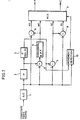
- Fig. 1 is a block diagram showing a construction of a conventional movement adaptation type YC separating circuit disclosed in Japanese Patent Laying-Open JP-A-61123295.
- a composite video signal is converted to an 8-bit digital signal by an A/D converter 1.
- This digital signal is delayed by 1H (H being a horizontal sync signal period) in a line memory 2 and it is further delayed by 524H's in a frame memory 3.
- Input and output signals of the line memory 2 supplied to a subtracter 4, where the output signal of the line memory 2 is subtracted from the input signal of the line memory 2.
- a luminance signal component is offset in the output of the subtracter 4 by line correlation of the composite television signal.
- the output of the horizontal bandpass filter 5 is supplied as a first chrominance signal MC to a mixing circuit 9.
- the output signal of the A/D converter 1 and the first chrominance signal MC are supplied to a subtracter 6, where the first chrominance signal MC is subtracted from the output signal of the A/D converter 1.
- the chrominance signal component is offset in the composite television signal as the output signal of the A/D converter 1, whereby a first luminance signal MY is obtained.
- This first luminance signal MY is supplied to the mixing circuit 9.
- the output signal of the A/D converter 1 and the output signal of the frame memory 3 are supplied to a subtracter 7, where the output signal of the frame memory 3 is subtracted from the output signal of the A/D converter 1.
- the output signal of the frame memory 3 is a signal delayed exactly by one frame from the composite video signal outputted from the A/D converter 1
- a luminance signal component is offset in the output signal of the A/D converter 1 by frame correlation so that a second chrominance signal SC is obtained.
- This second chrominance signal SC is supplied to the mixing circuit 9.
- the output signal of the A/D converter 1 and the second chrominance signal SC are supplied to a subtracter 8, where the second chrominance signal SC is subtracted from the output signal of the A/D converter 1.
- the color signal component is offset in the composite video signal outputted from the A/D converter 1, whereby a second luminance signal SY is obtained.
- the second luminance signal SY is supplied to the mixing circuit 9.
- the output signal of the A/D converter 1 and the output signal of the frame memory 3 are supplied to a movement detecting circuit 10.
- This movement detecting circuit 10 evaluates a difference signal between frames of the composite video signal and determines based on the difference signal whether an image formed by the present composite video signal is a moving picture or a still picture.
- the output of the movement detecting circuit 10 is supplied to the mixing circuit 9.
- the mixing circuit 9 selects the first luminance signal MY and the first chrominance signal MC separated by utilizing the line correlation and outputs those signals as the luminance signal Y and the chrominance signal C if the output of the movement detecting circuit 10 indicates a moving picture.
- the mixing circuit 9 selects the second luminance signal SY and the second chrominance signal SC separated by utilizing the frame correlation and outputs those signals as the luminance signal Y and the chrominance signal C.
- the movement detecting circuit 10 may be constructed to output a detection signal having its level changing in an analog manner according to the moving condition of the picture and the mixing circuit 9 may be constructed to mix the first luminance signal MY and the second luminance signal SY with a ratio according to the level of the detection output and to mix the first chrominance signal MC and the second chrominance signal SC with that ratio.
- the above mentioned movement adaptation type YC separating circuit makes it possible to separate a luminance signal and a chrominance signal with high qualities without causing any mixture or remaining of those signals.
- still picture reproduction processing is conventionally carried out by using a dedicated frame memory. More specifically, a frame memory other than the frame memory provided in the movement adaptation type YC separating circuit has to be separately provided to carry out still picture reproduction processing.
- An object of the present invention is to effect still picture reproduction with an inexpensive construction in a television receiver including a movement adaptation type YC separating circuit.
- processing for still picture reproduction is carried out by using the delay means included in the luminance signal/chrominance signal separating means (the movement adaptation type YC separating circuit).
- the delay means provided in the luminance signal/color signal separating means is also used for still picture reproduction and consequently processing for still picture reproduction can be carried out with an inexpensive construction.
- Fig. 1 is a block diagram showing a construction of a conventional movement adaptation type YC separating circuit.
- Fig. 2 is a block diagram showing a construction of a Y/C separation circuit.
- Fig. 3 is a block diagram showing a construction of an embodiment of the present invention.
- Fig. 4 is a block diagram showing a construction of a further embodiment of the present invention.
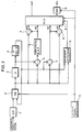
- the circuit shown in Fig. 2 has the same construction as that of the conventional movement adaptation type YC separating circuit shown in Fig. 1, except for the below described features. The portions corresponding to those in Fig. 1 are denoted by the same reference numerals and the description thereof is not repeated.
- the circuit shown in Fig. 2 further comprises a switch circuit 11, a control signal generating circuit 12 and a chroma inverter circuit 13 in order that the movement adaptation type YC separating circuit may have a still picture reproducing function.
- the switch circuit 11 selects either an output signal of the A/D converter 1 or an output signal of the frame memory 3 and outputs the selected signal to the line memory 2.
- the control signal generating circuit 12 generates a control signal in response to an instruction of still picture reproduction from a still picture reproduction switch (not shown) manually operated by the user for example.
- the control signal is supplied to the switch circuit 11, the mixing circuit 9 and the chroma inverter 13. Switching operation of the switch circuit 11 is controlled in response to the control signal.
- the mixing circuit 9 is constructed to select and output the first luminance signal MY and the first chrominance signal MC in response to the above mentioned control signal.
- the chroma inverter circuit 13 is enabled in response to the above mentioned control signal to invert the polarity of the chrominance signal for one frame (525H's) so as to maintain a sequence of a chrominance subcarrier for two frames in still picture reproduction.
- the control signal from the control signal generating circuit 12 is at low (L) level and the switch circuit 11 is at the position selecting the output signal of the A/D converter 1. Accordingly, the movement adaptation type YC separating circuit operates in the same manner as in the conventional circuit shown in Fig. 1. In this case, the chroma inverter circuit 13 is disabled and does not operate. Thus, the chroma inverter 13 outputs the chrominance signal C supplied from the mixing circuit 9 as it is.
- the control signal from the control signal generating circuit 12 rises to high (H) level. Consequently, the switch circuit 11 is turned to the position for selecting the output signal of the frame memory 3. As a result, the switch circuit 11, the line memory 2 and the frame memory 3 constitute a circulating circuit of one frame (525H's).
- the first and second luminance signals MY and SY and the first and second chrominance signals MC and SC supplied to the mixing circuit 9 form a circulation signal of one frame, namely, a still picture signal. Since the two signals inputted to the subtracter 7 are the same, the chrominance signals have the same phase and it is not possible to separate a luminance signal and a chrominance signal in a three-dimensional manner by utilizing frame correlation. Accordingly, it is necessary to separate a luminance signal and a chrominance signal in a two-dimensional manner by utilizing only line correlation in a field in still picture reproduction. Therefore, according to this embodiment, when the control signal from the control signal generating circuit 12 attains H level, the mixing circuit 9 e.g. selects and outputs only the first luminance signal MY and the first chrominance signal MC obtained by the forced two-dimensional processing, independent of the output of the movement detecting circuit 10.
- the phase sequence for two frames could not be maintained without any processing.
- the chroma inverter circuit 13 is enabled in response to the control signal of H level, whereby the phase of the chrominance signal is inverted for each frame by the chroma inverter circuit 13.
- the sequence of the chrominance signal for two frames can be maintained and a continuous chrominance subcarrier can be obtained.
- the timing of switching between L level and H level of the control signal from the control signal generating circuit 12 is selected to be coincident with a vertical blanking period. Accordingly, the timing of switching of the switch circuit 11, namely, the timing of generation of discontinuous points of the phases of the chrominance subcarrier coincides with the timing of inversion of the phase by the chroma inverter circuit 13 and thus a perfect continuity of the chrominance signal can be maintained.
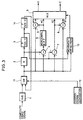
- a circulating circuit of one frame (525H's) is formed in still picture reproduction; however, if a circulating circuit of two frames (1050H's) is formed by additionally providing another frame memory, a luminance signal and a chrominance signal can be separated in a three-dimensional manner in still picture reproduction. In such a case, a still picture of a higher quality can be obtained because there are no problems such as cross color or dot interference in a two-dimensional separation. Further, in such a case, the chroma inverter circuit 13 needs not be provided since a sequence of the chrominance subcarrier of the two-frame period can be always maintained.
- an embodiment for still picture reproduction by using a composite video signal obtained from a circulating circuit of two frames will be described.
- a frame memory 14 is additionally provided between the frame memory 3 and the switch circuit 11.
- This frame memory 14 is constructed to delay an input signal by a one-frame period (525H's).
- the other construction is the same as that of the embodiment shown in Fig. 2 and the corresponding portions are denoted by the same reference numerals.
- a circulating circuit of two frames is formed by the switch circuit 11, the line memory 2, the frame memory 3 and the frame memory 14 in still picture reproduction. Accordingly, the two composite video signals inputted to the subtracter 7 in still picture reproduction have timings different from each other by one frame and consequently a chrominance signal can be separated by frame correlation. Similarly, a luminance signal can be separated in the subtracter 8.
- the mixing circuit 9 is controlled by the output of the movement detecting circuit 10. More specifically, in still picture reproduction, the mixing circuit 9 selects and outputs the first luminance signal MY and the first chrominance signal MC if there is a movement in the composite video signals of two frames circulating in the above mentioned circulating circuit, and it selects and outputs the second luminance signal SY and the second chrominance signal SC if there is no movement in the composite video signals. As a result, in the embodiment shown in Fig. 3, the control signal from the control signal generating circuit 12 is not applied to the mixing circuit 9.
- the output signal of the switch circuit 11 is delayed by a one-frame period (525H's) in the frame memory 15 and then delayed by 1H in the line memory 16, and further delayed by 524H's in the frame memory 17.
- the output signal of the frame memory 17 is applied to the switch circuit 11 together with the output signal of the A/D converter 1.
- the subtracter 4 separates a chrominance signal by the input/output signals of the line memory 16.
- the subtracter 6 subtracts the output signal of the horizontal bandpass filter 5 from the output signal of the frame memory 15, so as to separate a luminance signal.
- the output signal of the switch circuit 11, the output signal of the frame memory 15 and the output signal of the frame memory 17 are supplied to coefficient multipliers 18, 19 and 20, respectively.
- the coefficient multipliers 18 and 20 multiply the respective input signals by -1/4 and the coefficient multiplier 19 multiplies the input signal by 1/2.
- the output signals of those coefficient multipliers 18, 19 and 20 are supplied to an adder 21, where those signals are added.
- the frame memory 15, the line memory 16, the frame memory 17, the coefficient multipliers 18 to 20 and the adder 21 constitute a three-dimensional comb filter, which separates the second chrominance signal SC.
- the subtracter 8 subtracts the second chrominance signal SC from the output signal of the frame memory 15, thereby obtaining the second luminance signal SY.
- the other construction is the same as that of the embodiment shown in Fig. 2.
- a circulating circuit of two frames is formed by the switch circuit 11, the frame memory 15, the line memory 16 and the frame memory 17 in still picture reproduction.
- a luminance signal and a chrominance signal is two-dimensionally separated and three-dimensionally separated from the composite video signal obtained from the circulating circuit.
- the mixing circuit 9 in still picture reproduction can be controlled by the detection signal from the movement detecting circuit 10 so as to select and output either the first luminance signal MY, the first chrominance signal MC or the second luminance signal SY, the second chrominance signal SC.
- a luminance signal and a chrominance signal can be separated three-dimensionally by utilizing frame correlation even in still picture reproduction as described above and consequently a still picture of high quality can be obtained without any adverse effect such as cross color or dot interference.
- the chroma inverter circuit 13 used in the circuit of Fig. 2 needs not be provided.
Description
- The present invention relates generally to television receivers, and more particularly to television receivers having a still picture reproducing function.
- A combined line- and field-comb filter having a still picture reproducing function is known from US-A-4 701 785, in which the line- and field-delays are arranged in parallel during still picture reproduction.
- Conventional methods for separating a luminance signal (Y signal) and a chrominance signal (C signal) from a composite television signal include a method using a movement adaptation type YC separating circuit.
- Fig. 1 is a block diagram showing a construction of a conventional movement adaptation type YC separating circuit disclosed in Japanese Patent Laying-Open JP-A-61123295. Referring to Fig. 1, a composite video signal is converted to an 8-bit digital signal by an A/D converter 1. This digital signal is delayed by 1H (H being a horizontal sync signal period) in a
line memory 2 and it is further delayed by 524H's in aframe memory 3. Input and output signals of theline memory 2 supplied to asubtracter 4, where the output signal of theline memory 2 is subtracted from the input signal of theline memory 2. A luminance signal component is offset in the output of thesubtracter 4 by line correlation of the composite television signal. However, since a high frequency component of the luminance signal in the vertical direction of the screen remains, this component is removed by ahorizontal bandpass filter 5. The output of thehorizontal bandpass filter 5 is supplied as a first chrominance signal MC to amixing circuit 9. The output signal of the A/D converter 1 and the first chrominance signal MC are supplied to asubtracter 6, where the first chrominance signal MC is subtracted from the output signal of the A/D converter 1. As a result, the chrominance signal component is offset in the composite television signal as the output signal of the A/D converter 1, whereby a first luminance signal MY is obtained. This first luminance signal MY is supplied to themixing circuit 9. - In the meantime, the output signal of the A/D converter 1 and the output signal of the
frame memory 3 are supplied to asubtracter 7, where the output signal of theframe memory 3 is subtracted from the output signal of the A/D converter 1. Since the output signal of theframe memory 3 is a signal delayed exactly by one frame from the composite video signal outputted from the A/D converter 1, a luminance signal component is offset in the output signal of the A/D converter 1 by frame correlation so that a second chrominance signal SC is obtained. This second chrominance signal SC is supplied to themixing circuit 9. The output signal of the A/D converter 1 and the second chrominance signal SC are supplied to asubtracter 8, where the second chrominance signal SC is subtracted from the output signal of the A/D converter 1. As a result, the color signal component is offset in the composite video signal outputted from the A/D converter 1, whereby a second luminance signal SY is obtained. The second luminance signal SY is supplied to themixing circuit 9. - The output signal of the A/D converter 1 and the output signal of the
frame memory 3 are supplied to amovement detecting circuit 10. Thismovement detecting circuit 10 evaluates a difference signal between frames of the composite video signal and determines based on the difference signal whether an image formed by the present composite video signal is a moving picture or a still picture. The output of themovement detecting circuit 10 is supplied to themixing circuit 9. Themixing circuit 9 selects the first luminance signal MY and the first chrominance signal MC separated by utilizing the line correlation and outputs those signals as the luminance signal Y and the chrominance signal C if the output of themovement detecting circuit 10 indicates a moving picture. On the other hand, if the output of themovement detecting circuit 10 indicates a still picture, themixing circuit 9 selects the second luminance signal SY and the second chrominance signal SC separated by utilizing the frame correlation and outputs those signals as the luminance signal Y and the chrominance signal C. - The
movement detecting circuit 10 may be constructed to output a detection signal having its level changing in an analog manner according to the moving condition of the picture and themixing circuit 9 may be constructed to mix the first luminance signal MY and the second luminance signal SY with a ratio according to the level of the detection output and to mix the first chrominance signal MC and the second chrominance signal SC with that ratio. - The above mentioned movement adaptation type YC separating circuit makes it possible to separate a luminance signal and a chrominance signal with high qualities without causing any mixture or remaining of those signals.
- If still picture reproduction is to be effected in a television receiver comprising a movement adaptation type YC separation circuit as described above, still picture reproduction processing is conventionally carried out by using a dedicated frame memory. More specifically, a frame memory other than the frame memory provided in the movement adaptation type YC separating circuit has to be separately provided to carry out still picture reproduction processing.
- An object of the present invention is to effect still picture reproduction with an inexpensive construction in a television receiver including a movement adaptation type YC separating circuit.
- This object is realized by the features of claim 1.
- Thus, according to the present invention, processing for still picture reproduction is carried out by using the delay means included in the luminance signal/chrominance signal separating means (the movement adaptation type YC separating circuit).
- According to the present invention, the delay means provided in the luminance signal/color signal separating means is also used for still picture reproduction and consequently processing for still picture reproduction can be carried out with an inexpensive construction.
- The foregoing and other objects, features, aspects and advantages of the present invention will become more apparent from the following detailed description of the present invention when taken in conjunction with the accompanying drawings.
- Fig. 1 is a block diagram showing a construction of a conventional movement adaptation type YC separating circuit.
- Fig. 2 is a block diagram showing a construction of a Y/C separation circuit.
- Fig. 3 is a block diagram showing a construction of an embodiment of the present invention.
- Fig. 4 is a block diagram showing a construction of a further embodiment of the present invention.
- The circuit shown in Fig. 2 has the same construction as that of the conventional movement adaptation type YC separating circuit shown in Fig. 1, except for the below described features. The portions corresponding to those in Fig. 1 are denoted by the same reference numerals and the description thereof is not repeated. The circuit shown in Fig. 2 further comprises a
switch circuit 11, a controlsignal generating circuit 12 and achroma inverter circuit 13 in order that the movement adaptation type YC separating circuit may have a still picture reproducing function. Theswitch circuit 11 selects either an output signal of the A/D converter 1 or an output signal of theframe memory 3 and outputs the selected signal to theline memory 2. The controlsignal generating circuit 12 generates a control signal in response to an instruction of still picture reproduction from a still picture reproduction switch (not shown) manually operated by the user for example. The control signal is supplied to theswitch circuit 11, themixing circuit 9 and thechroma inverter 13. Switching operation of theswitch circuit 11 is controlled in response to the control signal. Themixing circuit 9 is constructed to select and output the first luminance signal MY and the first chrominance signal MC in response to the above mentioned control signal. Thechroma inverter circuit 13 is enabled in response to the above mentioned control signal to invert the polarity of the chrominance signal for one frame (525H's) so as to maintain a sequence of a chrominance subcarrier for two frames in still picture reproduction. - Next, operation of the circuit shown in Fig. 2 will be described.
- First, in normal reproduction, the control signal from the control
signal generating circuit 12 is at low (L) level and theswitch circuit 11 is at the position selecting the output signal of the A/D converter 1. Accordingly, the movement adaptation type YC separating circuit operates in the same manner as in the conventional circuit shown in Fig. 1. In this case, thechroma inverter circuit 13 is disabled and does not operate. Thus, thechroma inverter 13 outputs the chrominance signal C supplied from themixing circuit 9 as it is. - Next, when the still picture reproduction switch (not shown) is pressed, the control signal from the control
signal generating circuit 12 rises to high (H) level. Consequently, theswitch circuit 11 is turned to the position for selecting the output signal of theframe memory 3. As a result, theswitch circuit 11, theline memory 2 and theframe memory 3 constitute a circulating circuit of one frame (525H's). - Accordingly, the first and second luminance signals MY and SY and the first and second chrominance signals MC and SC supplied to the
mixing circuit 9 form a circulation signal of one frame, namely, a still picture signal. Since the two signals inputted to thesubtracter 7 are the same, the chrominance signals have the same phase and it is not possible to separate a luminance signal and a chrominance signal in a three-dimensional manner by utilizing frame correlation. Accordingly, it is necessary to separate a luminance signal and a chrominance signal in a two-dimensional manner by utilizing only line correlation in a field in still picture reproduction. Therefore, according to this embodiment, when the control signal from the controlsignal generating circuit 12 attains H level, themixing circuit 9 e.g. selects and outputs only the first luminance signal MY and the first chrominance signal MC obtained by the forced two-dimensional processing, independent of the output of themovement detecting circuit 10. - As to the chrominance signal selected by the
mixing circuit 9, the phase sequence for two frames could not be maintained without any processing. However, thechroma inverter circuit 13 is enabled in response to the control signal of H level, whereby the phase of the chrominance signal is inverted for each frame by thechroma inverter circuit 13. As a result, the sequence of the chrominance signal for two frames can be maintained and a continuous chrominance subcarrier can be obtained. - The timing of switching between L level and H level of the control signal from the control
signal generating circuit 12 is selected to be coincident with a vertical blanking period. Accordingly, the timing of switching of theswitch circuit 11, namely, the timing of generation of discontinuous points of the phases of the chrominance subcarrier coincides with the timing of inversion of the phase by thechroma inverter circuit 13 and thus a perfect continuity of the chrominance signal can be maintained. - In the above described circuit, a circulating circuit of one frame (525H's) is formed in still picture reproduction; however, if a circulating circuit of two frames (1050H's) is formed by additionally providing another frame memory, a luminance signal and a chrominance signal can be separated in a three-dimensional manner in still picture reproduction. In such a case, a still picture of a higher quality can be obtained because there are no problems such as cross color or dot interference in a two-dimensional separation. Further, in such a case, the
chroma inverter circuit 13 needs not be provided since a sequence of the chrominance subcarrier of the two-frame period can be always maintained. Next, an embodiment for still picture reproduction by using a composite video signal obtained from a circulating circuit of two frames will be described. - In the embodiment shown in Fig. 3, a
frame memory 14 is additionally provided between theframe memory 3 and theswitch circuit 11. Thisframe memory 14 is constructed to delay an input signal by a one-frame period (525H's). The other construction is the same as that of the embodiment shown in Fig. 2 and the corresponding portions are denoted by the same reference numerals. According to the embodiment shown in Fig. 3, a circulating circuit of two frames is formed by theswitch circuit 11, theline memory 2, theframe memory 3 and theframe memory 14 in still picture reproduction. Accordingly, the two composite video signals inputted to thesubtracter 7 in still picture reproduction have timings different from each other by one frame and consequently a chrominance signal can be separated by frame correlation. Similarly, a luminance signal can be separated in thesubtracter 8. Thus, in the embodiment shown in Fig. 3, it is possible to separate a luminance signal and a chrominance signal two-dimensionally by utilizing line correlation and to separate a luminance signal and a color signal three-dimensionally by utilizing frame correlation. Accordingly, even in still picture reproduction, the mixingcircuit 9 is controlled by the output of themovement detecting circuit 10. More specifically, in still picture reproduction, the mixingcircuit 9 selects and outputs the first luminance signal MY and the first chrominance signal MC if there is a movement in the composite video signals of two frames circulating in the above mentioned circulating circuit, and it selects and outputs the second luminance signal SY and the second chrominance signal SC if there is no movement in the composite video signals. As a result, in the embodiment shown in Fig. 3, the control signal from the controlsignal generating circuit 12 is not applied to themixing circuit 9. - Next, still another embodiment for forming a circulating circuit of two frames in still picture reproduction will be described with reference to Fig. 4. In the embodiment shown in Fig. 4, the output signal of the
switch circuit 11 is delayed by a one-frame period (525H's) in theframe memory 15 and then delayed by 1H in theline memory 16, and further delayed by 524H's in theframe memory 17. The output signal of theframe memory 17 is applied to theswitch circuit 11 together with the output signal of the A/D converter 1. Thesubtracter 4 separates a chrominance signal by the input/output signals of theline memory 16. Thesubtracter 6 subtracts the output signal of thehorizontal bandpass filter 5 from the output signal of theframe memory 15, so as to separate a luminance signal. The output signal of theswitch circuit 11, the output signal of theframe memory 15 and the output signal of theframe memory 17 are supplied to coefficientmultipliers coefficient multiplier 19 multiplies the input signal by 1/2. The output signals of thosecoefficient multipliers adder 21, where those signals are added. Theframe memory 15, theline memory 16, theframe memory 17, thecoefficient multipliers 18 to 20 and theadder 21 constitute a three-dimensional comb filter, which separates the second chrominance signal SC. Thesubtracter 8 subtracts the second chrominance signal SC from the output signal of theframe memory 15, thereby obtaining the second luminance signal SY. The other construction is the same as that of the embodiment shown in Fig. 2. In the embodiment shown in Fig. 4, a circulating circuit of two frames is formed by theswitch circuit 11, theframe memory 15, theline memory 16 and theframe memory 17 in still picture reproduction. In still picture reproduction, a luminance signal and a chrominance signal is two-dimensionally separated and three-dimensionally separated from the composite video signal obtained from the circulating circuit. In the embodiment of Fig. 4, similarly to the embodiment of Fig. 3, the mixingcircuit 9 in still picture reproduction can be controlled by the detection signal from themovement detecting circuit 10 so as to select and output either the first luminance signal MY, the first chrominance signal MC or the second luminance signal SY, the second chrominance signal SC. - According to the embodiment shown in Fig. 3 or Fig. 4, a luminance signal and a chrominance signal can be separated three-dimensionally by utilizing frame correlation even in still picture reproduction as described above and consequently a still picture of high quality can be obtained without any adverse effect such as cross color or dot interference. In addition, the
chroma inverter circuit 13 used in the circuit of Fig. 2 needs not be provided.
Claims (3)
- A television receiver having a still picture reproducing function, comprising:luminance signal/chrominance signal separating means for separating a luminance signal and a chrominance signal from a composite video signal, said luminance signal/chrominance signal separating means including delay means (2, 3, 14, 15, 16, 17) having a first delay element for one horizontal scanning periode delay, a second delay element for one frame period delay, and a third delay element for one frame period delay, said first, second and third delay elements being connected in series, said delay means for delaying said composite video signal successively through the respective delay elements, thereby outputting a plurality of composite video signals having different prescribed delay times,first extracting means (4, 6) for evaluating an input signal and an output signal of said delay means and extracting a first luminance signal and a first chrominance signal based on line correlation of the composite video signal,second-extracting means (7, 8, 18, 19, 20, 21) for evaluating an input signal and an output signal of said delay means and extracting a second luminance signal and a second chrominance signal based on frame correlation of the composite video signal,a movement detecting circuit (10) for detecting a movement of a picture, anda mixing circuit (9) in which a mixing ratio of said first and second luminance signals and the mixing ratio of said first and second chrominance signals are controlled in response to an output of said movement detecting circuit; control signal generating means (12) for generating a control signal in response to an instruction of still picture reproduction; andswitch means (11) provided at the stage preceding the application of said composite video signal to said first delay means, controlled in response to said control signal for short-circuiting input and output terminals of said delay means thereby forming a circulating circuit in which said composite signal circulates in said delay means in still picture reproduction, and for otherwise passing said composite video signal to said delay means,said luminance signal/chrominance signal separating means separating the luminance signal and the chrominance signal by means of said first extracting means and said second extracting means based on an output obtained from said circulating circuit and mixing the separated signals by means of said mixing circuit to output the mixed signal in still picture reproduction.
- A television receiver according to claim (1), wherein the switching operation of said switch means (11) is carried out in a vertical blanking period of said composite video signal.
- A television receiver according to claim 1, wherein said mixing circuit (9) in still picture reproduction selects and outputs either one of said first and second luminance signals (MYSY) and either one of said first and second chrominance signals (MC, SC) in response to the output of said movement detecting circuit (10).
Applications Claiming Priority (2)
| Application Number | Priority Date | Filing Date | Title |
|---|---|---|---|
| JP28322588 | 1988-11-09 | ||
| JP283225/88 | 1988-11-09 |
Publications (3)
| Publication Number | Publication Date |
|---|---|
| EP0368314A2 EP0368314A2 (en) | 1990-05-16 |
| EP0368314A3 EP0368314A3 (en) | 1992-04-29 |
| EP0368314B1 true EP0368314B1 (en) | 1997-01-22 |
Family
ID=17662712
Family Applications (1)
| Application Number | Title | Priority Date | Filing Date |
|---|---|---|---|
| EP89120793A Expired - Lifetime EP0368314B1 (en) | 1988-11-09 | 1989-11-09 | Television receiver |
Country Status (6)
| Country | Link |
|---|---|
| US (1) | US4994900A (en) |
| EP (1) | EP0368314B1 (en) |
| KR (1) | KR0130762B1 (en) |
| CA (1) | CA2002555C (en) |
| DE (1) | DE68927700T2 (en) |
| ES (1) | ES2099065T3 (en) |
Families Citing this family (13)
| Publication number | Priority date | Publication date | Assignee | Title |
|---|---|---|---|---|
| US5146334A (en) * | 1989-02-27 | 1992-09-08 | Canon Kabushiki Kaisha | Video signal processing device for image editing using memory |
| JP2884590B2 (en) * | 1989-04-12 | 1999-04-19 | ソニー株式会社 | Video signal transmission / reception system, video signal reception device, and video signal transmission / reception method |
| KR940005178B1 (en) * | 1989-10-14 | 1994-06-11 | 미쯔비시 덴끼 가부시끼가이샤 | Motion adaptive luminance signal and color signal separating filter |
| US5541669A (en) * | 1990-03-29 | 1996-07-30 | Mitsubishi Denki Kabushiki Denki | Motion adaptive luminance signal and color signal separation filter |
| US5475445A (en) * | 1990-04-03 | 1995-12-12 | Mitsubishi Denki Kabushiki Kaisha | Motion adaptive luminance signal and color signal separation filter |
| KR960016852B1 (en) * | 1990-05-23 | 1996-12-21 | 삼성전자 주식회사 | Motion adaptive chrominance processing circuit |
| US5166788A (en) * | 1990-06-29 | 1992-11-24 | Samsung Electronics Co., Ltd. | Motion signal processor |
| JPH04170891A (en) * | 1990-11-05 | 1992-06-18 | Toshiba Corp | Three-dimensional y/c separation circuit |
| DE69126946T2 (en) * | 1990-11-05 | 1997-11-27 | Toshiba Kawasaki Kk | Luminance / chrominance isolation circuit |
| JP3278187B2 (en) * | 1991-03-14 | 2002-04-30 | 三菱電機株式会社 | Motion adaptive luminance signal color signal separation filter |
| US5959683A (en) * | 1997-06-26 | 1999-09-28 | Xerox Corporation | System to remove artifacts in a digital image derived from a television signal |
| US6031581A (en) * | 1997-06-26 | 2000-02-29 | Xerox Corporation | System for removing color bleed in a television image adapted for digital printing |
| JP4870528B2 (en) * | 2006-11-17 | 2012-02-08 | オリンパス株式会社 | Solid-state imaging device |
Family Cites Families (6)
| Publication number | Priority date | Publication date | Assignee | Title |
|---|---|---|---|---|
| JPS585632B2 (en) * | 1975-09-08 | 1983-02-01 | 松下電器産業株式会社 | Frame memory hand warmer |
| US4626895A (en) * | 1984-08-09 | 1986-12-02 | Rca Corporation | Sampled data video signal chrominance/luminance separation system |
| JPS61123295A (en) * | 1984-11-20 | 1986-06-11 | Nec Home Electronics Ltd | Y/c separation circuit of color television signal |
| US4701785A (en) * | 1986-10-27 | 1987-10-20 | Rca Corporation | Frame comb filter having freeze frame feature |
| JPH0813120B2 (en) * | 1987-04-30 | 1996-02-07 | 株式会社日立製作所 | Video signal processing circuit capable of reproducing still images |
| JP2562696B2 (en) * | 1988-11-09 | 1996-12-11 | 三洋電機株式会社 | Television receiver |
-
1989
- 1989-11-06 US US07/431,956 patent/US4994900A/en not_active Expired - Lifetime
- 1989-11-08 KR KR1019890016144A patent/KR0130762B1/en not_active IP Right Cessation
- 1989-11-08 CA CA002002555A patent/CA2002555C/en not_active Expired - Lifetime
- 1989-11-09 EP EP89120793A patent/EP0368314B1/en not_active Expired - Lifetime
- 1989-11-09 DE DE68927700T patent/DE68927700T2/en not_active Expired - Fee Related
- 1989-11-09 ES ES89120793T patent/ES2099065T3/en not_active Expired - Lifetime
Also Published As
| Publication number | Publication date |
|---|---|
| ES2099065T3 (en) | 1997-05-16 |
| EP0368314A3 (en) | 1992-04-29 |
| CA2002555C (en) | 1994-04-05 |
| DE68927700D1 (en) | 1997-03-06 |
| EP0368314A2 (en) | 1990-05-16 |
| US4994900A (en) | 1991-02-19 |
| KR0130762B1 (en) | 1998-04-11 |
| CA2002555A1 (en) | 1990-05-09 |
| DE68927700T2 (en) | 1997-08-07 |
| KR900008867A (en) | 1990-06-04 |
Similar Documents
| Publication | Publication Date | Title |
|---|---|---|
| US5333054A (en) | Apparatus for reducing noise in a video signal by processing a luminance and chrominance component | |
| EP0368314B1 (en) | Television receiver | |
| JP2601840B2 (en) | Video display device | |
| US4870482A (en) | Motion-adaptive type signal separator with data companding function | |
| US4851904A (en) | Motion detecting circuit for digital video signal | |
| US4939572A (en) | Video signal processing apparatus | |
| US5583579A (en) | Two-dimensional adaptation type luminance/chrominance signal separation apparatatus | |
| JPH06327030A (en) | Motion detecting circuit | |
| US5208662A (en) | Method of encoding color television signal and a circuit therefor | |
| US5194937A (en) | Television signal converting apparatus and method | |
| US5128750A (en) | Television signal converter for converting a high definition television signal into a television signal for display by a standard television receiver | |
| EP0464879B1 (en) | Apparatus for separating luminance and chrominance signals and the method thereof | |
| US5140410A (en) | Chrominance signal mixing circuit in a motion adaptive type signal separator | |
| US5170248A (en) | Motion-adaptive vertical contour compensator in television set | |
| KR920002274B1 (en) | Hd-tv compensative method | |
| US5305095A (en) | Method and circuit for encoding color television signal | |
| EP0364967B1 (en) | Luminance/chrominance signal separation circuit for pal color television signal | |
| JP2562696B2 (en) | Television receiver | |
| US4847679A (en) | Multiplex chrominance gain control and matrix using a single multiplier and a coefficient shift register | |
| KR0141129B1 (en) | Apparatus for separating chroma signal | |
| JPH0225596B2 (en) | ||
| JP3003178B2 (en) | Luminance signal color signal separation filter | |
| JPH05219522A (en) | Yc separator circuit | |
| JPH05219531A (en) | Motion signal generating circuit | |
| JPH04306997A (en) | Yc separator circuit in common use for moving adaptive processing |
Legal Events
| Date | Code | Title | Description |
|---|---|---|---|
| PUAI | Public reference made under article 153(3) epc to a published international application that has entered the european phase |
Free format text: ORIGINAL CODE: 0009012 |
|
| AK | Designated contracting states |
Kind code of ref document: A2 Designated state(s): DE ES FR GB IT |
|
| 17P | Request for examination filed |
Effective date: 19901228 |
|
| PUAL | Search report despatched |
Free format text: ORIGINAL CODE: 0009013 |
|
| AK | Designated contracting states |
Kind code of ref document: A3 Designated state(s): DE ES FR GB IT |
|
| 17Q | First examination report despatched |
Effective date: 19940525 |
|
| GRAG | Despatch of communication of intention to grant |
Free format text: ORIGINAL CODE: EPIDOS AGRA |
|
| GRAH | Despatch of communication of intention to grant a patent |
Free format text: ORIGINAL CODE: EPIDOS IGRA |
|
| GRAH | Despatch of communication of intention to grant a patent |
Free format text: ORIGINAL CODE: EPIDOS IGRA |
|
| GRAA | (expected) grant |
Free format text: ORIGINAL CODE: 0009210 |
|
| AK | Designated contracting states |
Kind code of ref document: B1 Designated state(s): DE ES FR GB IT |
|
| PG25 | Lapsed in a contracting state [announced via postgrant information from national office to epo] |
Ref country code: IT Free format text: LAPSE BECAUSE OF FAILURE TO SUBMIT A TRANSLATION OF THE DESCRIPTION OR TO PAY THE FEE WITHIN THE PRESCRIBED TIME-LIMIT;WARNING: LAPSES OF ITALIAN PATENTS WITH EFFECTIVE DATE BEFORE 2007 MAY HAVE OCCURRED AT ANY TIME BEFORE 2007. THE CORRECT EFFECTIVE DATE MAY BE DIFFERENT FROM THE ONE RECORDED. Effective date: 19970122 Ref country code: FR Effective date: 19970122 |
|
| REF | Corresponds to: |
Ref document number: 68927700 Country of ref document: DE Date of ref document: 19970306 |
|
| REG | Reference to a national code |
Ref country code: ES Ref legal event code: FG2A Ref document number: 2099065 Country of ref document: ES Kind code of ref document: T3 |
|
| EN | Fr: translation not filed | ||
| PLBE | No opposition filed within time limit |
Free format text: ORIGINAL CODE: 0009261 |
|
| STAA | Information on the status of an ep patent application or granted ep patent |
Free format text: STATUS: NO OPPOSITION FILED WITHIN TIME LIMIT |
|
| 26N | No opposition filed | ||
| REG | Reference to a national code |
Ref country code: GB Ref legal event code: IF02 |
|
| PGFP | Annual fee paid to national office [announced via postgrant information from national office to epo] |
Ref country code: ES Payment date: 20071127 Year of fee payment: 19 Ref country code: DE Payment date: 20071101 Year of fee payment: 19 |
|
| PGFP | Annual fee paid to national office [announced via postgrant information from national office to epo] |
Ref country code: GB Payment date: 20071107 Year of fee payment: 19 |
|
| GBPC | Gb: european patent ceased through non-payment of renewal fee |
Effective date: 20081109 |
|
| PG25 | Lapsed in a contracting state [announced via postgrant information from national office to epo] |
Ref country code: DE Free format text: LAPSE BECAUSE OF NON-PAYMENT OF DUE FEES Effective date: 20090603 |
|
| PG25 | Lapsed in a contracting state [announced via postgrant information from national office to epo] |
Ref country code: GB Free format text: LAPSE BECAUSE OF NON-PAYMENT OF DUE FEES Effective date: 20081109 |
|
| REG | Reference to a national code |
Ref country code: ES Ref legal event code: FD2A Effective date: 20081110 |
|
| PG25 | Lapsed in a contracting state [announced via postgrant information from national office to epo] |
Ref country code: ES Free format text: LAPSE BECAUSE OF NON-PAYMENT OF DUE FEES Effective date: 20081110 |