EP0367707B1 - A circuit arrangement for adjusting offset voltages associates with operational amplifiers - Google Patents
A circuit arrangement for adjusting offset voltages associates with operational amplifiers Download PDFInfo
- Publication number
- EP0367707B1 EP0367707B1 EP89480153A EP89480153A EP0367707B1 EP 0367707 B1 EP0367707 B1 EP 0367707B1 EP 89480153 A EP89480153 A EP 89480153A EP 89480153 A EP89480153 A EP 89480153A EP 0367707 B1 EP0367707 B1 EP 0367707B1
- Authority
- EP
- European Patent Office
- Prior art keywords
- circuit arrangement
- operational amplifier
- coupled
- fet
- voltage
- Prior art date
- Legal status (The legal status is an assumption and is not a legal conclusion. Google has not performed a legal analysis and makes no representation as to the accuracy of the status listed.)
- Expired - Lifetime
Links
- 239000000758 substrate Substances 0.000 claims description 10
- 239000004020 conductor Substances 0.000 claims description 5
- 230000008878 coupling Effects 0.000 claims 3
- 238000010168 coupling process Methods 0.000 claims 3
- 238000005859 coupling reaction Methods 0.000 claims 3
- 238000000034 method Methods 0.000 description 22
- 239000003990 capacitor Substances 0.000 description 9
- 230000009897 systematic effect Effects 0.000 description 5
- 230000000694 effects Effects 0.000 description 3
- 238000005516 engineering process Methods 0.000 description 3
- 230000003321 amplification Effects 0.000 description 2
- 238000006243 chemical reaction Methods 0.000 description 2
- 238000003199 nucleic acid amplification method Methods 0.000 description 2
- 239000007787 solid Substances 0.000 description 2
- 230000003068 static effect Effects 0.000 description 2
- 206010035148 Plague Diseases 0.000 description 1
- XUIMIQQOPSSXEZ-UHFFFAOYSA-N Silicon Chemical compound [Si] XUIMIQQOPSSXEZ-UHFFFAOYSA-N 0.000 description 1
- 241000607479 Yersinia pestis Species 0.000 description 1
- 238000010420 art technique Methods 0.000 description 1
- 230000003749 cleanliness Effects 0.000 description 1
- 238000009826 distribution Methods 0.000 description 1
- 238000004519 manufacturing process Methods 0.000 description 1
- 238000005070 sampling Methods 0.000 description 1
- 229910052710 silicon Inorganic materials 0.000 description 1
- 239000010703 silicon Substances 0.000 description 1
- 238000003860 storage Methods 0.000 description 1
- 238000009966 trimming Methods 0.000 description 1
Images

Classifications
-
- H—ELECTRICITY
- H03—ELECTRONIC CIRCUITRY
- H03F—AMPLIFIERS
- H03F3/00—Amplifiers with only discharge tubes or only semiconductor devices as amplifying elements
- H03F3/45—Differential amplifiers
- H03F3/45071—Differential amplifiers with semiconductor devices only
- H03F3/45479—Differential amplifiers with semiconductor devices only characterised by the way of common mode signal rejection
- H03F3/45928—Differential amplifiers with semiconductor devices only characterised by the way of common mode signal rejection using IC blocks as the active amplifying circuit
- H03F3/45968—Differential amplifiers with semiconductor devices only characterised by the way of common mode signal rejection using IC blocks as the active amplifying circuit by offset reduction
-
- H—ELECTRICITY
- H03—ELECTRONIC CIRCUITRY
- H03F—AMPLIFIERS
- H03F2203/00—Indexing scheme relating to amplifiers with only discharge tubes or only semiconductor devices as amplifying elements covered by H03F3/00
- H03F2203/45—Indexing scheme relating to differential amplifiers
- H03F2203/45214—Offset in a differential amplifier being reduced by control of the substrate voltage, the voltage being either fixed or variable
-
- H—ELECTRICITY
- H03—ELECTRONIC CIRCUITRY
- H03F—AMPLIFIERS
- H03F2203/00—Indexing scheme relating to amplifiers with only discharge tubes or only semiconductor devices as amplifying elements covered by H03F3/00
- H03F2203/45—Indexing scheme relating to differential amplifiers
- H03F2203/45342—Indexing scheme relating to differential amplifiers the AAC comprising control means on a back gate of the AAC
Definitions
- the present invention relates to operational amplifiers in general and more particularly to a circuit arrangement which negates the offset voltages associated with said amplifiers.
- Operational amplifiers may be used for a wide variety of purposes, such as those in which high gain amplification is required.
- a conventional high gain operational amplifier consists of at least an input and an output stage. A signal provided at the input stage is amplified and outputted at the output stage.
- capacitance mismatch between supposedly identical silicon gate MOS capacitors is also a function of process variations. Systematic offset is caused by mismatches between cascaded stages of an op. amp. and is present even with perfect device matching.
- Document GB A-2,100,540 discloses a reference voltage generator comprising a differential amplifier with a negative feedback loop and having an input offset determining the output voltage.
- the output of the amplifier is fed back to the inverting input either directly or via a potential divider and a reference voltage level is connected to the non-inverting input.
- the output voltage is determined (relative to the reference voltage level) by the difference in threshold voltages of the input transistors, this difference being substantially independent of the temperature variations.
- the feedback connection may include a controlling amplifier element having its control electrode which is coupled to the output of the operational amplifier, its first output electrode which is coupled to a power supply terminal, and its second output electrode which is coupled to the inverting input of the operational amplifier.
- the second output electrode of said controlling amplifier element may be coupled to the inverting input of the operational amplifier through a voltage divider which is connected to said output electrode of the controlling amplifier element. But for precision amplifier, it is necessary to cancel all offset voltages.
- the offset voltage is stored during one clock cycle and substracted during another clock cycle. Even though this technique works well for its intented purpose, its main drawback is that it requires clocks and sampling techniques to cancel the offset. As a result, the switched capacitor approach does not allow the op amp to amplify signals approaching the frequency limit of the technology. In addition, the switched capacitor technique is a sampled one and does not allow for continuous amplification. Also switched capacitor circuits consume large amounts of area, and the clock signals can introduce noise into the signal.
- the circuit arrangement includes an op amp biased to virtual ground and a negative feedback conductor.
- the op amp includes an input stage having a - pair of differential FET devices with the substrate electrode of one of the devices connected to the conductor, and an intentional offset voltage (Vosi) having a magnitude greater than that of the op amp normal offset voltage (Vos) is placed within the input stage.
- the polarity of the intentional offset voltage is opposite to the polarity of the op amp.
- the circuit arrangement provides a compensating signal which can be used to negate the offset voltage of other op amps.
- Vosi is generated by dissimilar paired differential devices.
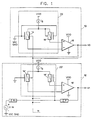
- Fig. 1 is a schematic of a circuit arrangement that generates a control voltage (Vo) which is used to compensate offsetting voltages in one or more operational amplifiers.
- Vo control voltage
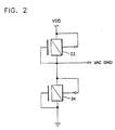
- Fig. 2 shows a circuit arrangement for generating an AC ground signal.
- Fig. 3 shows an equivalent circuit for Fig. 1 circuit arrangements. It is helpful in understanding the present invention.
- Fig. 1 shows a circuit arrangement which includes the teachings of the present invention.
- the circuit arrangement is comprised of a voltage generator 10 connected to circuit arrangement 12.
- Voltage generator 10 generates control voltage Vo which drives FET device 14′ and similar connected devices so that the threshold voltages of 14′ and said similar connected FET devices cancel (i.e., negate) the offset voltage which is associated with circuit arrangement 12.
- the voltage generator 10 is an improved operational amplifier which includes a partial operational amplifier (op amp) 18 and a partial differential input stage 20 that is adjusted in accordance with the teaching of the present invention.
- Partial operational amplifier 18 can include a plurality of amplifying stages interconnected in a conventional topology. Since multistage operational amplifiers are well known, applicant elects to show the other stages of the op amp that follow input stage 20 as a single block 18. Since the loading of differential input pairs within differential amplifiers are well known, the applicant also elects to show the load devices of the input stage of voltage generator 10 imbedded in block 18.
- Amplifier 18 includes a power terminal which is connected to a power supply Vdd, a control terminal which is connected to a ground potential and an output terminal which provides the output control voltage (Vo).
- Amplifier 18 has a negative input terminal and a positive input terminal.
- the input stage 20 comprises of a current source I s which is connected to power supply Vdd.
- current source I s is formed from P-channel devices or the like configured in a conventional topology.
- the differential input stage includes FET devices 14 and 16 which are connected in parallel and in series with current source I s In the preferred embodiment of this invention the FET devices are P channel enhancement mode devices.
- P-channel device 14 has its substrate electrode (identified by an arrow) connected to the output (Vo) of amplifier 18.
- the drain electrode of FET device 14 is connected to the negative input terminal of amplifier 18.
- the source electrode of FET device 14 is connected to I s and its gate electrode is connected to a bias voltage V ac ground.
- FET device 16 has its gate electrode connected to V ac ground.
- the substrate electrode and the source electrode of FET device 16 are connected to I s and the drain electrode is connected to the positive terminal of amplifier 18.
- P-channel devices 14 and 16 are matched pairs located in separate N-wells. The devices are fabricated so that the below-listed equation 1 is satisfied. (1) Vosi >
- V osi can be created.
- the geometries of devices 14 and 16 are used to provide Vosi.
- the width-to-length ratio of FET device 14 is greater than that of FET device 16.
- the introduced offset V osi is summed with the natural offset voltage V os which is present in voltage generator and op amp 10 such that the polarity of the net offset voltage in 10 is always opposite the polarity of the input terminals to 10 with respect to Vo. This eliminates the possibility of latch-up in device 14 caused by a net offset voltage with the same polarity as the input terminals to 10 with respect to Vo.
- the threshold voltage (Vt) of FET device 14 changes (i.e., adjusts) to cancel the net offset voltage caused by the intentional induced voltage V osi and the natural offset voltage Vos.
- Vt threshold voltage
- the control voltage Vo is used to negate the offset voltage of the op amp comprised of 18′ and 20′.
- the said op amp has characteristics similar to the op amp comprised of 18 and 20 and is positioned in close proximity thereto.
- CMOS technology is used for generating the op amps.
- the circuit arrangement 12 includes partial op amp 18′ and partial input stage 20′.
- the input stage is comprised of current source I s ′ and FET devices 14′ and 16′. The relationship between these components is similar to the relationship previously described for like components in input stage 20.
- Zin and Zf represent input and feedback circuitry respectively.
- the combination of Zin and Zf control the gain and the frequency response characteristics of circuit arrangement 12. Since the use of input and feedback circuitry to control the gain and frequency response of circuit arrangements using op amps is well known, applicant elects to show the input and feedback circuitry as single blocks Zin and Zf, respectively.
- Vin represents the input signal which is coupled into the amplifier.
- the input signal (Vin) is amplified and is outputted as V1.
- the circuit arrangement 12 can function as a sample and hold circuit. For example, if circuit arrangement 12 is a sample and hold circuit, then Zin and Zf are comprised of switched capacitors (capacitor elements switched using transistors and clock signals).
- Fig. 2 shows a circuit arrangement which can be used to provide bias voltage V ac ground to the respective terminals of Fig. 1.
- Fig. 3 shows an equivalent circuit for Fig. 1. This equivalent circuit is helpful in understanding the operation of the invention.
- components in Fig. 3 which are identical to components in Figs. 1 and 2 are identified by common alphanumeric characters with double and triple prime notations indicating that these components are in Fig. 3.
- the partial op amps 18 ⁇ and 18′′′ are biased by a feedback configuration and an a.c. ground voltage (Vac gnd).
- Vosi, Vos, V′osi′ and V′os′ represent offset voltages which have been intentionally introduced in the input stages of op amps 18 ⁇ and 18′′′.
- Vos and V′os′ represent the maximum naturally occurring equivalent offset voltage.
- the geometries of the input differential pair devices can be selected to provide a desired intentionally introduced offset voltage.
- positive input transistors 14 ⁇ and 14′′′ each has its own isolated N-well.
- Vt Vt0+K1 [ (0 ⁇ - Vbs) 1/2 -(0 ⁇ ) 1/2 ]
- V b the potential between the bulk (substrate) and source of the device
- K1 is a body effect coefficient of Vt
- 0 ⁇ is a surface potential of strong inversion
- Vt represents the device threshold voltage
- Vto represents the device natural threshold voltage
- V osi is always a positive value biased as shown in Fig. 3, and it is always greater than or equal to the magnitude of the maximum naturally-occurring equivalent offset voltage (Vos).
- Vosi is greater than the absolute value of V os maximum. As described above, this V osi is created by selecting the proper geometry of differential pair input devices (such as 14 ⁇ , 16 ⁇ , etc.).
- the quiescent operating point of the op amp that includes amplifier 18 ⁇ is when Vo ⁇ causes a Vbs that results in a shift in the threshold voltage of 14 ⁇ exactly equal to the sum of V osi and V os .
- the output voltage Vo ⁇ can then be made available to the N-well (bulk) terminal with positive input transistor (such as 14′′′, etc.) of another identical copy and physically close op amp that includes amplifier 18′′′ in order to cause the same negating effect.
- the offset voltage of the said op amp is approximately negated and thus its output voltage V1 is not affected by the offset voltage present in the op amp.
- This assumes that physically close op amps have identical offset voltages. It is obvious that V osi is identical for both op amps containing amplifiers 18 ⁇ and 18′′′ since it is the result of design and the design of the two op amps is identical.
Landscapes
- Engineering & Computer Science (AREA)
- Power Engineering (AREA)
- Amplifiers (AREA)
Description
- The present invention relates to operational amplifiers in general and more particularly to a circuit arrangement which negates the offset voltages associated with said amplifiers.
- Operational amplifiers may be used for a wide variety of purposes, such as those in which high gain amplification is required. A conventional high gain operational amplifier consists of at least an input and an output stage. A signal provided at the input stage is amplified and outputted at the output stage.
- A significant disadvantage that plagues all operational amplifiers is voltage offset. This offset is present even in the absence of an input signal. As set forth in an article entitled "MOS Operational Amplifier Design," a tutorial overview, by Paul R. Gray et al, IEEE Journal Solid State Circuits, Vol. SC-17, pp. 969-982, Dec. 1982, the offset voltage of an op amp consists of two components, random offset and systematic offset. Random offset results from mismatches due to process variations in supposedly identical pairs of devices. In MOSFET op amps random offset is primarily due to threshold voltage mismatch. Threshold voltage mismatch is a function of process cleanliness and uniformity.
- Similarly, capacitance mismatch between supposedly identical silicon gate MOS capacitors is also a function of process variations. Systematic offset is caused by mismatches between cascaded stages of an op. amp. and is present even with perfect device matching.
- Document GB A-2,100,540 discloses a reference voltage generator comprising a differential amplifier with a negative feedback loop and having an input offset determining the output voltage. The output of the amplifier is fed back to the inverting input either directly or via a potential divider and a reference voltage level is connected to the non-inverting input. The output voltage is determined (relative to the reference voltage level) by the difference in threshold voltages of the input transistors, this difference being substantially independent of the temperature variations. The feedback connection may include a controlling amplifier element having its control electrode which is coupled to the output of the operational amplifier, its first output electrode which is coupled to a power supply terminal, and its second output electrode which is coupled to the inverting input of the operational amplifier. The second output electrode of said controlling amplifier element may be coupled to the inverting input of the operational amplifier through a voltage divider which is connected to said output electrode of the controlling amplifier element. But for precision amplifier, it is necessary to cancel all offset voltages.
- The prior art describes several techniques for cancelling op. amp. offset voltages. Some of these techniques are set forth in the following articles : H. Schmidt, "Electronic Analog/Digital Conversions," New York, Van Nostrand-Reinhold, 1970, R. Poujors, B. Boylac, D. Barbier and J. M. Ittel, "Low Level MOS Transistor Amplifier Using Storage Techniques," ISSCC Dig. Tech. Papers, Feb. 1975 and US Patent 4,439,693. Primarily, these methods used switched capacitor circuits.
- Usually the offset voltage is stored during one clock cycle and substracted during another clock cycle. Even though this technique works well for its intented purpose, its main drawback is that it requires clocks and sampling techniques to cancel the offset. As a result, the switched capacitor approach does not allow the op amp to amplify signals approaching the frequency limit of the technology. In addition, the switched capacitor technique is a sampled one and does not allow for continuous amplification. Also switched capacitor circuits consume large amounts of area, and the clock signals can introduce noise into the signal.
- As can be seen from the above description, these techniques are dynamic. Dynamic techniques can be costly and undesirable for some applications. Thus, there is need for a static method to eliminate offset voltages in CMOS operational amplifiers.
- In the US patent 4,462,002, trimming circuits for precision amplifier are disclosed. In this invention, imbalances in the potential appearing across the drain electrodes of source coupled FET transistors arranged in a differential amplifier configuration tend to produce input offset voltages. The drain electrodes of the transistors are coupled to a current mirror load for converting balanced signals to a single ended output which in turn is applied to a common source amplifier, the input offset may be nulled by differentially adjusting the drain current of the common source amplifier against the source current of the differential stage.
- Another prior art method which is used to negate offset voltage is the so-called "common centroid geometries." This method is particularly suited for matching silicon-gate MOS capacitors and is described by Paul R. Gray, James L. McCreary, "ALL-MOS Charge Redistribution Analog-to-Digital Conversion Techniques - Part 1," IEEE Solid State Circuits, Vol. SC-10, pp. 371-379, Dec. 1975. However, published data (see O. H. Shade, Jr. "BIMOS Micropower Integrated Circuits," IEEE Solid-State Circuits, Vol. SC-13, pp; 791-7998, Dec. 1978 and O. H. Shade, Jr. and E. J. Kramner, "A Low-Voltage BIMOS Op Amp, " IEEE Solid-State Circuits, Vol. SC-16, pp. 661-668, Dec. 1981) seems to indicate that large-geometry common-centroid matched transistors are also capable of significantly improving transistor mismatch distributions. The large geometries effectively eliminate the second order effects of process variations. Hence, process variations can be approximated as first order gradients within a physically close area.
- Even though the common centroid geometries work well with two-terminal capacitors, using it with three-terminal transistors can require intricate physical designs. Large common centroid geometries consume large amounts of area. In addition, the common centroid method does not compensate for systematic offset. Finally, prior art techniques that compensate for systematic offsets require sacrificing low noise and best frequency response under capacitive loading.
- Instead of cancelling the op. ampl. offset voltages, it may possible to produce a desired offset voltage at the input of a circuit. The invention disclosed in the European patent application EP A-289-181 published on November, 2nd 1988, relates to an integrated circuit technique for producing a desired offset voltage at the input of a circuit using differential circuit with controllable offset. The circuit implemented enables to make the offset voltage independent of all factors except the reference voltage.
- It is a general object of the present invention to provide a circuit arrangement as defined in the appended claims, which compensates for offsetting voltage in an op amp. The circuit arrangement includes an op amp biased to virtual ground and a negative feedback conductor. The op amp includes an input stage having a - pair of differential FET devices with the substrate electrode of one of the devices connected to the conductor, and an intentional offset voltage (Vosi) having a magnitude greater than that of the op amp normal offset voltage (Vos) is placed within the input stage. The polarity of the intentional offset voltage is opposite to the polarity of the op amp. The circuit arrangement provides a compensating signal which can be used to negate the offset voltage of other op amps.
- In one feature of the invention Vosi is generated by dissimilar paired differential devices.
- The foregoing and other objects, features and advantages of this invention will be more fully described in the accompanying drawings.
- Fig. 1 is a schematic of a circuit arrangement that generates a control voltage (Vo) which is used to compensate offsetting voltages in one or more operational amplifiers.
- Fig. 2 shows a circuit arrangement for generating an AC ground signal.
- Fig. 3 shows an equivalent circuit for Fig. 1 circuit arrangements. It is helpful in understanding the present invention.
- Fig. 1 shows a circuit arrangement which includes the teachings of the present invention. The circuit arrangement is comprised of a
voltage generator 10 connected tocircuit arrangement 12. As will be described subsequently, depending on the circuitries which are used to implement Zin and Zf circuit arrangement 12 can be made into a sample and hold circuit or the like. The dotted line in Fig. 1 indicates that additional circuit arrangements such as 12 can be connected tovoltage generator 10.Voltage generator 10 generates control voltage Vo which drivesFET device 14′ and similar connected devices so that the threshold voltages of 14′ and said similar connected FET devices cancel (i.e., negate) the offset voltage which is associated withcircuit arrangement 12. - The
voltage generator 10 is an improved operational amplifier which includes a partial operational amplifier (op amp) 18 and a partialdifferential input stage 20 that is adjusted in accordance with the teaching of the present invention. Partialoperational amplifier 18 can include a plurality of amplifying stages interconnected in a conventional topology. Since multistage operational amplifiers are well known, applicant elects to show the other stages of the op amp that followinput stage 20 as asingle block 18. Since the loading of differential input pairs within differential amplifiers are well known, the applicant also elects to show the load devices of the input stage ofvoltage generator 10 imbedded inblock 18.Amplifier 18 includes a power terminal which is connected to a power supply Vdd, a control terminal which is connected to a ground potential and an output terminal which provides the output control voltage (Vo).Amplifier 18 has a negative input terminal and a positive input terminal. Theinput stage 20 comprises of a current source Is which is connected to power supply Vdd. Preferably, current source Is is formed from P-channel devices or the like configured in a conventional topology. The differential input stage includesFET devices channel device 14 has its substrate electrode (identified by an arrow) connected to the output (Vo) ofamplifier 18. The drain electrode ofFET device 14 is connected to the negative input terminal ofamplifier 18. The source electrode ofFET device 14 is connected to Is and its gate electrode is connected to a bias voltage Vac ground. Similarly,FET device 16 has its gate electrode connected to Vac ground. The substrate electrode and the source electrode ofFET device 16 are connected to Is and the drain electrode is connected to the positive terminal ofamplifier 18. Preferably, P-channel devices 
where Vosi is an intentionally introduced offset voltage and Vos represents the normal offset voltage in voltage generator andop amp 10. - There exists a variety of different ways in which Vosi can be created. In the preferred embodiment of this invention the geometries of
devices FET device 14 is greater than that ofFET device 16. As a result of this relationship, the introduced offset Vosi is summed with the natural offset voltage Vos which is present in voltage generator andop amp 10 such that the polarity of the net offset voltage in 10 is always opposite the polarity of the input terminals to 10 with respect to Vo. This eliminates the possibility of latch-up indevice 14 caused by a net offset voltage with the same polarity as the input terminals to 10 with respect to Vo. By connecting the substrate terminal ofFET device 14 to the output ofamplifier 18 the threshold voltage (Vt) ofFET device 14 changes (i.e., adjusts) to cancel the net offset voltage caused by the intentional induced voltage Vosi and the natural offset voltage Vos. The net result is that the output voltage Vo is free from any offset voltage and is used to negate offset voltages in similar type operational amplifiers. - Still referring to Fig. 1, the control voltage Vo is used to negate the offset voltage of the op amp comprised of 18′ and 20′. Preferably, the said op amp has characteristics similar to the op amp comprised of 18 and 20 and is positioned in close proximity thereto. Preferably, CMOS technology is used for generating the op amps. Of course, other types of technologies could be used for designing the op amps without deviating from the scope or spirit of the present invention. The
circuit arrangement 12 includespartial op amp 18′ andpartial input stage 20′. The input stage is comprised of current source Is′ andFET devices 14′ and 16′. The relationship between these components is similar to the relationship previously described for like components ininput stage 20. Zin and Zf represent input and feedback circuitry respectively. The combination of Zin and Zf control the gain and the frequency response characteristics ofcircuit arrangement 12. Since the use of input and feedback circuitry to control the gain and frequency response of circuit arrangements using op amps is well known, applicant elects to show the input and feedback circuitry as single blocks Zin and Zf, respectively. Vin represents the input signal which is coupled into the amplifier. The input signal (Vin) is amplified and is outputted as V1. Depending on the circuitry which is selected for Zin and Zf, thecircuit arrangement 12 can function as a sample and hold circuit. For example, ifcircuit arrangement 12 is a sample and hold circuit, then Zin and Zf are comprised of switched capacitors (capacitor elements switched using transistors and clock signals). An example of capacitive circuits which could be used for Zin and Zf are set forth in Fig. 7 of copending application EP-A-0 347 359 filed June 17, 1988, and assigned to the assignee of the present invention. The subject application is incorporated herein by reference. - Fig. 2 shows a circuit arrangement which can be used to provide bias voltage Vac ground to the respective terminals of Fig. 1. The circuit arrangement includes two P-
channel transistors 
- Fig. 3 shows an equivalent circuit for Fig. 1. This equivalent circuit is helpful in understanding the operation of the invention. For simplicity, components in Fig. 3 which are identical to components in Figs. 1 and 2 are identified by common alphanumeric characters with double and triple prime notations indicating that these components are in Fig. 3. As is seen in Fig. 3, the
partial op amps 18˝ and 18‴ are biased by a feedback configuration and an a.c. ground voltage (Vac gnd). - Z˝in and Z˝f perform the same functions as previously described Zin and Zf. Of particular interest are Vosi, Vos, V′osi′ and V′os′. Vosi and V′osi′ represent offset voltages which have been intentionally introduced in the input stages of
op amps 18˝ and 18‴. Likewise, Vos and V′os′ represent the maximum naturally occurring equivalent offset voltage. As stated previously, the geometries of the input differential pair devices (such as 14˝, 16˝, etc.) can be selected to provide a desired intentionally introduced offset voltage. As stated previously,positive input transistors 14˝ and 14‴ each has its own isolated N-well. The N-well (bulk) terminals are externally biased to adjustable voltage Vo˝ which is always less than the common source voltages of the transistors. The threshold voltages of 14˝, 14‴, etc. are, therefore, a function of Vo. A mathematical expression for the relationship is set forth in Equation 2 below.
where Vb is the potential between the bulk (substrate) and source of the device, K1 is a body effect coefficient of Vt, 0̸ is a surface potential of strong inversion, Vt represents the device threshold voltage and Vto represents the device natural threshold voltage. - It is claimed that if the polarity of the total net offset voltage comprised of Vos and Vosi is opposite the polarity of the input terminals to the op amp with respect to Vo (i.e., if Vosi ≧|Vos|), there exists some voltage Vo that can shift the threshold voltage by exactly the said total net offset voltage and effectively cancel or negate all offset voltage in the op amp. If the total net offset voltage was allowed to have the same polarity as the said input terminals (i.e., if Vosi < |Vos|), then it would be required that Vt would have to be shifted below Vto in order to negate the total net offset voltage. This is not possible with the constraint that the N-well bulk or substrate voltage must always be less than or equal to the common source voltage in order to avoid latch-up. To solve this problem, more offset has been introduced intentionally into the op amp. This voltage is identified as Vosi in Fig. 3. Vosi is always a positive value biased as shown in Fig. 3, and it is always greater than or equal to the magnitude of the maximum naturally-occurring equivalent offset voltage (Vos). This maximum equivalent offset voltage can be determined from the process used in manufacturing the devices. Thus, Vosi is greater than the absolute value of Vos maximum. As described above, this Vosi is created by selecting the proper geometry of differential pair input devices (such as 14˝, 16˝, etc.).
- Still referring to Fig. 3, since the positive input terminals of the op amps are shorted to a common a.c. ground input, the equivalent offset voltages are shown in series with the positive input terminal. The op amp that includes
amplifier 18˝ is configured such that its output provides negative feedback to the N-well (bulk) terminal oftransistor 14˝. Therefore, the quiescent operating point of the op amp that includesamplifier 18˝ is when Vo˝ causes a Vbs that results in a shift in the threshold voltage of 14˝ exactly equal to the sum of Vosi and Vos. The output voltage Vo˝ can then be made available to the N-well (bulk) terminal with positive input transistor (such as 14‴, etc.) of another identical copy and physically close op amp that includesamplifier 18‴ in order to cause the same negating effect. The offset voltage of the said op amp is approximately negated and thus its output voltage V1 is not affected by the offset voltage present in the op amp. This, of course, assumes that physically close op amps have identical offset voltages. It is obvious that Vosi is identical for both opamps containing amplifiers 18˝ and 18‴ since it is the result of design and the design of the two op amps is identical. It is also obvious that the systematic component of Vos is identical for both op amps since it is also the result of design. Although the remainder of the offset is random within any given sample op amp, this offset approximately tracks systematically between both opamps containing amplifiers 18˝ and 18‴. This concludes the description of the present invention which sets forth a new static device and method that eliminates total equivalent offset voltages in CMOS operational amplifiers.
Claims (7)
- A circuit arrangement (10) for adjusting offset voltages associated with operational amplifiers comprising a first operational amplifier (18) having an output (V0), and a first input stage (20) coupled to said operational amplifier, said input stage having a pair of FET devices (14, 16) for providing a first offset voltage having a magnitude which is greater than the magnitude of a natural offset voltage of said operational amplifier, said circuit arrangement characterized in that it further comprises:
a connecting means for coupling the output of said operational amplifier to a substrate electrode of one of said FET devices so that the algebraic sum of the first offset voltage, threshold voltage of said one of said FET devices and the natural offset voltage is essentially zero. - The circuit arrangement set forth in claim 1 further including a current source (Is) coupled to the first input stage (20) and a power supply (VDD) coupled to said current source.
- The circuit arrangement set forth in claim 2 further including a circuit network for providing an AC ground signal (VAC GND) coupled to said input stage.
- The circuit arrangement of any one of the previous claims further including:- at least a second operational amplifier (18′) having an output terminal (V1), a positive and negative input terminals,- a current source (Is′) and a power supply (VDD) coupled to said current source,- a second input stage (20′) coupled to said second operational amplifier, said second input stage having a pair of FET devices (14′, 16′) whose first FET device (14′) is coupled to the negative output terminal of said second operational amplifier, and whose second FET device (16′) is coupled to the current source and arranged in parallel with said first FET,- a first conductor coupling the second FET device to the output terminal of said second operational amplifier (18′),- a second conductor coupling the second FET device to the positive input terminal of said second operational amplifier, and- a third conductor interconnecting a substrate electrode of said first FET device to the first operational amplifier (18).
- The circuit arrangement of claim 4 further including means for providing an AC ground signal (VAC GND) coupled to said first FET device (14′).
- The circuit arrangement of claim 3 or 5 wherein the AC ground signal (VAC GND) includes two P-enhancement mode devices (22, 24) connected in series between a power supply (VDD) and the ground, wherein each device has its gate electrode connected to its drain electrode and its substrate electrode connected to its source electrode so that the AC ground signal (VAC GND) is equal to half the power supply (VDD/2).
- The circuit arrangement of any one of the previous claims wherein the FET devices include P-channel enhancement mode devices.
Applications Claiming Priority (2)
| Application Number | Priority Date | Filing Date | Title |
|---|---|---|---|
| US265113 | 1988-10-31 | ||
| US07/265,113 US4948992A (en) | 1988-10-31 | 1988-10-31 | Static method to negate offset voltages in CMOS operational amplifiers |
Publications (3)
| Publication Number | Publication Date |
|---|---|
| EP0367707A2 EP0367707A2 (en) | 1990-05-09 |
| EP0367707A3 EP0367707A3 (en) | 1991-03-20 |
| EP0367707B1 true EP0367707B1 (en) | 1995-02-01 |
Family
ID=23009059
Family Applications (1)
| Application Number | Title | Priority Date | Filing Date |
|---|---|---|---|
| EP89480153A Expired - Lifetime EP0367707B1 (en) | 1988-10-31 | 1989-09-26 | A circuit arrangement for adjusting offset voltages associates with operational amplifiers |
Country Status (4)
| Country | Link |
|---|---|
| US (1) | US4948992A (en) |
| EP (1) | EP0367707B1 (en) |
| JP (1) | JPH0738544B2 (en) |
| DE (1) | DE68920949T2 (en) |
Cited By (1)
| Publication number | Priority date | Publication date | Assignee | Title |
|---|---|---|---|---|
| EP3343333A1 (en) * | 2016-12-30 | 2018-07-04 | LG Display Co., Ltd. | Touch power circuit having operational amplifier and touch display device using the same |
Families Citing this family (13)
| Publication number | Priority date | Publication date | Assignee | Title |
|---|---|---|---|---|
| JP2760543B2 (en) * | 1989-02-10 | 1998-06-04 | 株式会社東芝 | Multiple feedback circuit |
| US5220207A (en) * | 1991-09-03 | 1993-06-15 | Allegro Microsystems, Inc. | Load current monitor for MOS driver |
| FI97655C (en) * | 1995-04-05 | 1997-01-27 | Nokia Telecommunications Oy | Linear RF detector with offset compensation |
| US5726597A (en) * | 1996-08-30 | 1998-03-10 | Motorola, Inc. | Method and circuit for reducing offset voltages for a differential input stage |
| WO1999007067A1 (en) * | 1997-08-01 | 1999-02-11 | Lsi Logic Corporation | Offset adjustment of cmos matched pairs with body voltage |
| GB2336958B (en) | 1998-05-01 | 2003-04-23 | Sgs Thomson Microelectronics | Comparators |
| US6222395B1 (en) * | 1999-01-04 | 2001-04-24 | International Business Machines Corporation | Single-ended semiconductor receiver with built in threshold voltage difference |
| EP1024348B1 (en) * | 1999-01-28 | 2011-07-27 | Denso Corporation | Low-frequency noise removing method and a related CMOS sensing circuit |
| US6313691B1 (en) * | 1999-02-17 | 2001-11-06 | Elbrus International Limited | Method and apparatus for adjusting the static thresholds of CMOS circuits |
| EP1228121A1 (en) * | 1999-07-16 | 2002-08-07 | Aerojet-General Corporation | Amorphous polyether glycols based on bis-substituted oxetane monomers |
| DE10028460B4 (en) * | 2000-06-08 | 2009-02-12 | Schwarzer GmbH Meßgeräte für die Medizin | Integrated signal processing circuit |
| JP2004165649A (en) * | 2002-10-21 | 2004-06-10 | Matsushita Electric Ind Co Ltd | Semiconductor integrated circuit device |
| US9941852B1 (en) | 2016-09-28 | 2018-04-10 | Nxp Usa, Inc. | Operation amplifiers with offset cancellation |
Family Cites Families (12)
| Publication number | Priority date | Publication date | Assignee | Title |
|---|---|---|---|---|
| US3050673A (en) * | 1960-10-14 | 1962-08-21 | Ibm | Voltage holding circuit |
| JPS5384264U (en) * | 1976-12-15 | 1978-07-12 | ||
| JPS5396650A (en) * | 1977-02-02 | 1978-08-24 | Nec Corp | Automatic adjustment circuit for offset voltage |
| GB2100540B (en) * | 1978-03-08 | 1983-06-02 | Hitachi Ltd | Reference voltage generators |
| JPS5714216A (en) * | 1980-06-30 | 1982-01-25 | Mitsubishi Electric Corp | Input protecting circuit |
| US4365204A (en) * | 1980-09-08 | 1982-12-21 | American Microsystems, Inc. | Offset compensation for switched capacitor integrators |
| US4439693A (en) * | 1981-10-30 | 1984-03-27 | Hughes Aircraft Co. | Sample and hold circuit with improved offset compensation |
| US4462002A (en) * | 1982-05-24 | 1984-07-24 | Rca Corporation | Trimming circuits for precision amplifier |
| JPS59126319A (en) * | 1982-08-31 | 1984-07-20 | Toshiba Corp | Chopper type comparator |
| JPH0793553B2 (en) * | 1983-11-18 | 1995-10-09 | 株式会社日立製作所 | Switched capacitor filter |
| US4604584A (en) * | 1985-06-10 | 1986-08-05 | Motorola, Inc. | Switched capacitor precision difference amplifier |
| US4754169A (en) * | 1987-04-24 | 1988-06-28 | American Telephone And Telegraph Company, At&T Bell Laboratories | Differential circuit with controllable offset |
-
1988
- 1988-10-31 US US07/265,113 patent/US4948992A/en not_active Expired - Fee Related
-
1989
- 1989-08-11 JP JP1207111A patent/JPH0738544B2/en not_active Expired - Lifetime
- 1989-09-26 DE DE68920949T patent/DE68920949T2/en not_active Expired - Fee Related
- 1989-09-26 EP EP89480153A patent/EP0367707B1/en not_active Expired - Lifetime
Cited By (1)
| Publication number | Priority date | Publication date | Assignee | Title |
|---|---|---|---|---|
| EP3343333A1 (en) * | 2016-12-30 | 2018-07-04 | LG Display Co., Ltd. | Touch power circuit having operational amplifier and touch display device using the same |
Also Published As
| Publication number | Publication date |
|---|---|
| US4948992A (en) | 1990-08-14 |
| DE68920949T2 (en) | 1995-08-10 |
| JPH0738544B2 (en) | 1995-04-26 |
| DE68920949D1 (en) | 1995-03-16 |
| EP0367707A2 (en) | 1990-05-09 |
| JPH02131005A (en) | 1990-05-18 |
| EP0367707A3 (en) | 1991-03-20 |
Similar Documents
| Publication | Publication Date | Title |
|---|---|---|
| US4697152A (en) | Fully differential switched capacitor amplifier having autozeroed common-mode feedback | |
| EP0367707B1 (en) | A circuit arrangement for adjusting offset voltages associates with operational amplifiers | |
| US4543534A (en) | Offset compensated switched capacitor circuits | |
| EP0508360B1 (en) | Sampled band-gap voltage reference circuit | |
| US5124663A (en) | Offset compensation CMOS operational amplifier | |
| US5844442A (en) | Low voltage fully differential operational amplifier with improved common mode circuitry | |
| EP0295221B1 (en) | Cmos power operational amplifier | |
| US4794349A (en) | Fully differential, CMOS operational power amplifier | |
| Duisters et al. | A-90-dB THD rail-to-rail input opamp using a new local charge pump in CMOS | |
| EP1006648B1 (en) | Active compensating capacitive multiplier | |
| JPS63229509A (en) | Reference voltage generation circuit | |
| JPS6355108B2 (en) | ||
| JPS58500045A (en) | Bandgap reference voltage generation circuit and its generation method | |
| EP0158646B1 (en) | Switched capacitor circuits | |
| EP0478297B1 (en) | Wide-band differential amplifier using GM-cancellation | |
| EP0286347A2 (en) | Balanced output analog differential amplifier circuit | |
| Wu et al. | A CMOS transistor-only 8-b 4.5-Ms/s pipelined analog-to-digital converter using fully-differential current-mode circuit techniques | |
| US4585951A (en) | Precision triangle waveform generator | |
| Van Peteghem et al. | Micropower high-performance SC building block for integrated low-level signal processing | |
| US4912427A (en) | Power supply noise rejection technique for amplifiers | |
| US4884039A (en) | Differential amplifier with low noise offset compensation | |
| US5374859A (en) | Low power dual power supply high resolution comparator | |
| US4577162A (en) | Clocked gain stage having differential inputs and outputs | |
| US4647865A (en) | Parasitic insensitive switched capacitor input structure for a fully differential operational amplifier | |
| US5406220A (en) | Pole/zero compensation in cascode amplifiers |
Legal Events
| Date | Code | Title | Description |
|---|---|---|---|
| PUAI | Public reference made under article 153(3) epc to a published international application that has entered the european phase |
Free format text: ORIGINAL CODE: 0009012 |
|
| AK | Designated contracting states |
Kind code of ref document: A2 Designated state(s): DE FR GB |
|
| 17P | Request for examination filed |
Effective date: 19900820 |
|
| PUAL | Search report despatched |
Free format text: ORIGINAL CODE: 0009013 |
|
| AK | Designated contracting states |
Kind code of ref document: A3 Designated state(s): DE FR GB |
|
| 17Q | First examination report despatched |
Effective date: 19930709 |
|
| GRAA | (expected) grant |
Free format text: ORIGINAL CODE: 0009210 |
|
| AK | Designated contracting states |
Kind code of ref document: B1 Designated state(s): DE FR GB |
|
| REF | Corresponds to: |
Ref document number: 68920949 Country of ref document: DE Date of ref document: 19950316 |
|
| ET | Fr: translation filed | ||
| PGFP | Annual fee paid to national office [announced via postgrant information from national office to epo] |
Ref country code: FR Payment date: 19950911 Year of fee payment: 7 |
|
| PGFP | Annual fee paid to national office [announced via postgrant information from national office to epo] |
Ref country code: DE Payment date: 19950921 Year of fee payment: 7 |
|
| PLBE | No opposition filed within time limit |
Free format text: ORIGINAL CODE: 0009261 |
|
| STAA | Information on the status of an ep patent application or granted ep patent |
Free format text: STATUS: NO OPPOSITION FILED WITHIN TIME LIMIT |
|
| 26N | No opposition filed | ||
| PGFP | Annual fee paid to national office [announced via postgrant information from national office to epo] |
Ref country code: GB Payment date: 19960827 Year of fee payment: 8 |
|
| PG25 | Lapsed in a contracting state [announced via postgrant information from national office to epo] |
Ref country code: FR Effective date: 19960930 |
|
| PG25 | Lapsed in a contracting state [announced via postgrant information from national office to epo] |
Ref country code: DE Effective date: 19970603 |
|
| REG | Reference to a national code |
Ref country code: FR Ref legal event code: ST |
|
| REG | Reference to a national code |
Ref country code: FR Ref legal event code: ST |
|
| PG25 | Lapsed in a contracting state [announced via postgrant information from national office to epo] |
Ref country code: GB Free format text: LAPSE BECAUSE OF NON-PAYMENT OF DUE FEES Effective date: 19970926 |
|
| GBPC | Gb: european patent ceased through non-payment of renewal fee |
Effective date: 19970926 |