EP0366453A2 - Variabler Strom-Spannungs-Verstärker mit einem verstärkungsunabhängigen Prüfungsmodus - Google Patents
Variabler Strom-Spannungs-Verstärker mit einem verstärkungsunabhängigen Prüfungsmodus Download PDFInfo
- Publication number
- EP0366453A2 EP0366453A2 EP89311025A EP89311025A EP0366453A2 EP 0366453 A2 EP0366453 A2 EP 0366453A2 EP 89311025 A EP89311025 A EP 89311025A EP 89311025 A EP89311025 A EP 89311025A EP 0366453 A2 EP0366453 A2 EP 0366453A2
- Authority
- EP
- European Patent Office
- Prior art keywords
- amplifier
- test
- gain
- current
- adjustable
- Prior art date
- Legal status (The legal status is an assumption and is not a legal conclusion. Google has not performed a legal analysis and makes no representation as to the accuracy of the status listed.)
- Withdrawn
Links
Images
Classifications
-
- H—ELECTRICITY
- H03—ELECTRONIC CIRCUITRY
- H03F—AMPLIFIERS
- H03F3/00—Amplifiers with only discharge tubes or only semiconductor devices as amplifying elements
-
- G—PHYSICS
- G01—MEASURING; TESTING
- G01R—MEASURING ELECTRIC VARIABLES; MEASURING MAGNETIC VARIABLES
- G01R31/00—Arrangements for testing electric properties; Arrangements for locating electric faults; Arrangements for electrical testing characterised by what is being tested not provided for elsewhere
- G01R31/28—Testing of electronic circuits, e.g. by signal tracer
- G01R31/2832—Specific tests of electronic circuits not provided for elsewhere
- G01R31/2836—Fault-finding or characterising
-
- H—ELECTRICITY
- H03—ELECTRONIC CIRCUITRY
- H03G—CONTROL OF AMPLIFICATION
- H03G3/00—Gain control in amplifiers or frequency changers
- H03G3/02—Manually-operated control
Definitions
- the present invention generally relates to a precision current-to-voltage amplifier having an adjustable gain in the normal mode of operation and more particularly to one also having a test mode of operation wherein test signals can be injected into the amplifier to verify that it is still operating.
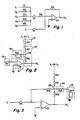
- a known current-to-voltage amplifier is shown in Figure 1.
- switch S1 In the normal mode of operation, switch S1 is closed and switch S2 is open.
- R8 can have almost any value but typically is between 100 ⁇ and 100M ⁇ . To monitor whether the amplifier is functioning properly, it can be operated in a test mode wherein switch S1 is open and switch S2 is closed.
- a test input current is applied by selecting from one of a series of voltage sources and corresponding resistors, V1 to V5 and R1 to R5, respectively.
- the values of V1 to V5 and R1 to R5 are varied so as to produce a range of test current values which when multiplied by do not exceed the output capability of op amp 20.
- test input current chosen depends upon the gain of the amplifier.
- R8 is variable and is typically chosen from a set of resistors of many different values depending upon the range of the current being amplified.
- a different test input current is required to test the operation of the amplifier without putting op amp 20 into saturation.
- V1-V5 voltage source values
- R1-R5 resistors
- the present invention relates to a current-to-voltage amplifier having a normal mode of operation wherein the amplifier has an adjustable gain (i.e., normal gain) and also having a test mode of operation wherein the amplifier has a fixed gain independent of the adjustable gain in the normal mode.
- the invention provides an easy way to verify the operation of the active component(s) of the amplifier and thus the amplifier itself, independent of the normal gain of the amplifier. This feature is particularly important since the gain of the amplifier can vary widely. In prior amplifiers, such as shown in Figure 1, the gain would need to be known to change the correct test input. This is not necessary in the present invention since in the test mode of operation, the gain of the amplifier is independent of the normal gain. Thus, only one test input is necessary, thereby reducing the complexity of the circuitry and the number of the components used therein.
- the invention in its broad form resides in precision current-to-voltage amplifier apparatus with on-line test capabilities having a normal amplification mode of operation wherein an input current (I i ) is amplified by an adjustable gain to produce an output voltage (V o ) corresponding thereto and also having a test mode of operation wherein the output voltage is independent of the normal amplification gain, said amplifier comprising: (a) an active component having an input to receive an input current, and providing an output voltage V o ; characterized by: (b) a first switch means connected between the input current and the active component; (c) a first adjustable amplification means connected in an amplifier configuration to the active component; (d) a test input divider connected to the output voltage such that the adjustable amplification means is connected to the output voltage through a portion of the test input divider; and (e) a second switch means connected between a test input and the test input divider, the second switch means and the first switch means not both being closed at the same time.
- the current-to-voltage amplifier as described herein comprises: an active component, preferably an op amp; a first switch means connected between the input current I i and the active component; and an adjustable amplification means, preferably a set of resistors which alternatively can be switched into the circuit or a variable resistor such as a potentiometer, connected to the active component in an amplifier configuration; and a test input divider connected between a second switch means and the amplifier output such that the adjustable amplification means is connected to the amplifier output through a portion of the test input divider, and wherein the second switch means is connected between the test input and the test input divider and the second switch means and the first switch means are not both closed at the same time.
- an active component preferably an op amp
- a first switch means connected between the input current I i and the active component
- an adjustable amplification means preferably a set of resistors which alternatively can be switched into the circuit or a variable resistor such as a potentiometer, connected to
- the active component and the adjustable amplification means are arranged in the standard amplifier configuration. If the active component is an op amp and the amplification means is a resistor, the resistor is connected between the negative input of the op amp and a mid portion of the test input divider.
- the test input divider comprises a plurality of resistors connected in series, preferably two resistors, one connected between the amplifier output and the adjustable amplification means and the other between the adjustable amplification means and the second switch which connects the test input to the amplifier circuit.
- the first switch In the normal mode of operational the first switch is closed, connecting the input to the amplifier and the second switch is open, disconnecting the test input from the amplifier.
- the amplifier gain is determined by the value of the adjustable amplification means and the second portion of the test input divider. If, however, the value of the test input divider is relatively small compared to the value of the adjustable amplification means, the amplification value is determined primarily by the value of the adjustable amplification means.
- the test input When the first switch is opened, the input is disconnected and when the second switch is closed, the test input is connected.
- the current through the first portion of the test input divider must equal the current through the second portion of the input test divider since no current flows through the adjustable amplification means.
- the amplitude of the test input current equals the amplifier output current.
- the two resistors of the test input divider are chosen to be equal so that the amplitudes of the test input voltage and the test output voltage are equal, if the op amp is working properly. If the op amp is not, the test input voltage Will not equal the test output voltage.
- the present invention provides an easy way to verify the operation of a precision current-to-voltage amplifier.
- a gain limiting means and a second adjustable amplification means are connected in series with each other and are connected to the first adjustable amplification means at the mid portion of the test input divider.
- the gain limiting means preferably is a resistor which prevents the op amp from saturating.
- the second adjustable amplification means is provided because it allows a fixed precision resistor to be substituted for the first adjustable amplification means, thereby providing a more accurate amplifier while at the same time providing the necessary adjustability in the gain of the amplifier.
- the present invention provides a current-to-voltage amplifier having a field adjustable gain in the normal mode of operation to accommodate different full scale ranges of input signals.
- the amplifier also has a test mode of operation with a fixed gain independent of the amplifier gain in the normal mode of operation which simplifies and facilitates the automatic testing of the amplifier and its functioning.
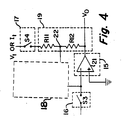
- the precision current-to-voltage amplifier uses an op amp 21 as the active component 15.
- the op amp has a very low input offset and input bias current characteristics such as an OPA111 made by Burr Brown.
- switches S3 and S4 can be used as the first switch means 16 and the second switch means 17, respectively. These switches determine whether the amplifier is operating in the normal mode or the test mode
- one resistor R10 is used as the adjustable amplification means 18 while R11 and R12 form the test input divider 19.
- This circuit can use a test current or a test voltage as the test input and preferably R11 is substantially equal to R12.
- switch S3 In the normal mode of operation, switch S3 is closed connecting input I i , and switch S4 is open disconnecting the test input (V t or I t ).
- R10 can be a potentiometer or a series of fixed resistors which alternately can be connected together in various configurations to form the desired value of R10.
- R10 typically varies from 1K to 100M ⁇ to obtain the amplification needed for the different ranges of input current I i . If R10 » R12, the gain of the amplifier in the normal mode is essentially R10 as can be seen from Equation (1).
- R11 R12 and are about 20K, although other values can be used.
- switch S3 is open disconnecting the input current I i
- switch S4 is closed, connecting the test input (V t or I t ).
- V t or I t the voltage at the common connection 22 of the test input divider and the adjustable amplification means is essentially ground. This is because no current flows through R10 and the inverting and positive inputs of op amp 21 are at the same voltage, namely ground.
- V o -R12 ⁇ I t or (2)
- V o - (3) depending upon whether a test voltage or test current is used.
- the output voltage V o in the test mode is independent of the adjustable gain R10.
- R12 R11
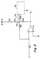
- FIG. 3 A second embodiment of the present invention is shown in Figure 3. In this configuration, rather than varying the value of R10, R10 is fixed and the value of R14 is varied.
- R14 is the second adjustable amplification means 23 while R13 is used as a gain limiting means 24.
- R13 is not necessary but as can be seen from Equation (4) it keeps the theoretical gain from becoming infinite, especially if R14 is switched out of the circuit.
- R14 is variable, being a potentiometer or a set of fixed resistors which can be connected in the circuit in a variety of configurations to obtain different values for R14. As long as R14 is a potentiometer, R13 is not necessary. R13, however, is needed if R14 is made from a plurality of resistors which are alternately switched into the circuit.
- Typical values for the resistors used to form R14 include 182 ⁇ , 221 ⁇ , 332 ⁇ , 715 ⁇ , 1.6K ⁇ , 5.6K ⁇ and 5.1M ⁇ . If R13 and R14 are removed from the circuit (i.e. they become very large), the circuit of Figure 3 becomes like the one in Figure 2 and Equation (4) reduces to Equation (1).
- the present invention has the added advantage that it can be used to measure the zero offset of op amp 21 due to bias currents and input offset voltages. This can be done by opening both switches S3 and S4. Then the measured output voltages is the zero offset voltage due to these error sources. Since superposition principles apply when switch S3 is closed and current I i flows, the value of the zero offset voltage can be subtracted from any output voltage measurement to obtain a more accurate reading.
Landscapes
- Engineering & Computer Science (AREA)
- General Engineering & Computer Science (AREA)
- Physics & Mathematics (AREA)
- General Physics & Mathematics (AREA)
- Power Engineering (AREA)
- Amplifiers (AREA)
- Testing Electric Properties And Detecting Electric Faults (AREA)
- Measurement Of Current Or Voltage (AREA)
Applications Claiming Priority (2)
| Application Number | Priority Date | Filing Date | Title |
|---|---|---|---|
| US262846 | 1988-10-26 | ||
| US07/262,846 US4896118A (en) | 1988-10-26 | 1988-10-26 | Variable gain current-to-voltage amplifier with gain independent test mode operation |
Publications (2)
| Publication Number | Publication Date |
|---|---|
| EP0366453A2 true EP0366453A2 (de) | 1990-05-02 |
| EP0366453A3 EP0366453A3 (de) | 1991-07-24 |
Family
ID=22999315
Family Applications (1)
| Application Number | Title | Priority Date | Filing Date |
|---|---|---|---|
| EP19890311025 Withdrawn EP0366453A3 (de) | 1988-10-26 | 1989-10-25 | Variabler Strom-Spannungs-Verstärker mit einem verstärkungsunabhängigen Prüfungsmodus |
Country Status (4)
| Country | Link |
|---|---|
| US (1) | US4896118A (de) |
| EP (1) | EP0366453A3 (de) |
| JP (1) | JPH0636485B2 (de) |
| KR (1) | KR900007169A (de) |
Families Citing this family (8)
| Publication number | Priority date | Publication date | Assignee | Title |
|---|---|---|---|---|
| US5689345A (en) * | 1996-01-31 | 1997-11-18 | R. R. Donnelley & Sons | Apparatus for testing amplifier for electromechanical gravure engraving machine |
| EP1441439A1 (de) * | 2003-01-23 | 2004-07-28 | Infineon Technologies AG | Analogverstärker mit Multiplexierungsfähigkeit |
| US20120206150A1 (en) * | 2009-08-27 | 2012-08-16 | Kyle David Holzer | Adjustable gain amplifier, automated test equipment and method for adjusting a gain of an amplifier |
| KR101354583B1 (ko) | 2010-09-17 | 2014-01-22 | 에스케이이노베이션 주식회사 | 누설전류를 발생시키지 않고 셀프 테스트 기능을 가진 절연저항 측정회로 |
| JP5859378B2 (ja) * | 2012-05-23 | 2016-02-10 | シャープ株式会社 | 電荷供給装置、チャージアンプ、チャージアンプ検査システム、センサシステム、および通信システム |
| CN103780303B (zh) * | 2012-10-24 | 2017-07-25 | 华为技术有限公司 | 光模块及其检测电路 |
| CN104391205B (zh) * | 2014-12-03 | 2017-04-19 | 中国航空综合技术研究所 | 一种增益可调的电压故障注入器 |
| CN105137327B (zh) * | 2015-10-10 | 2017-12-08 | 北京华峰测控技术有限公司 | 一种运算放大器检测补偿网络及其检测方法 |
Family Cites Families (1)
| Publication number | Priority date | Publication date | Assignee | Title |
|---|---|---|---|---|
| FR2088235B1 (de) * | 1970-05-29 | 1976-02-20 | Honeywell Bull Ste Ind Fr |
-
1988
- 1988-10-26 US US07/262,846 patent/US4896118A/en not_active Expired - Fee Related
-
1989
- 1989-10-25 KR KR1019890015397A patent/KR900007169A/ko not_active Withdrawn
- 1989-10-25 EP EP19890311025 patent/EP0366453A3/de not_active Withdrawn
- 1989-10-26 JP JP1277358A patent/JPH0636485B2/ja not_active Expired - Lifetime
Also Published As
| Publication number | Publication date |
|---|---|
| JPH02159579A (ja) | 1990-06-19 |
| KR900007169A (ko) | 1990-05-09 |
| US4896118A (en) | 1990-01-23 |
| JPH0636485B2 (ja) | 1994-05-11 |
| EP0366453A3 (de) | 1991-07-24 |
Similar Documents
| Publication | Publication Date | Title |
|---|---|---|
| US4034291A (en) | Electronic measuring instrument combining an oscilloscope and a digital multimeter | |
| US6255839B1 (en) | Voltage applied type current measuring circuit in an IC testing apparatus | |
| EP0023750A2 (de) | Abtast- und Halte-Schaltung | |
| US5034698A (en) | Dual-path wideband and precision data acquisition system | |
| EP0366453A2 (de) | Variabler Strom-Spannungs-Verstärker mit einem verstärkungsunabhängigen Prüfungsmodus | |
| US4677581A (en) | Multichannel, self-calibrating, analog input/output apparatus for generating and measuring DC stimuli | |
| US5414352A (en) | Parametric test circuit with plural range resistors | |
| US5448173A (en) | Triple-probe plasma measuring apparatus for correcting space potential errors | |
| US6069484A (en) | Source measure unit current preamplifier | |
| US5770956A (en) | Measurement amplifier | |
| US5528603A (en) | Apparatus and method for testing an integrated circuit using a voltage reference potential and a reference integrated circuit | |
| US6571598B2 (en) | Calibration circuit for use with a differential input preamplifier in a sensor system | |
| US3183446A (en) | Electrical signal comparator | |
| US4081744A (en) | Resistance bridge transducer conditioning circuit | |
| US3928795A (en) | Contact tester | |
| US4357544A (en) | Variable impedance circuit | |
| US3729676A (en) | Ratemeter | |
| US4300101A (en) | Multiple parallel input noise reduction system | |
| US4322679A (en) | Alternating current comparator bridge for resistance measurement | |
| JPH0357966A (ja) | 微小電流測定回路 | |
| US5877619A (en) | Battery-operated hand field-strength meter and method of null balancing same | |
| Hearn | A Precision Programmable Bipolar V/f Instrumentation Module | |
| US5625314A (en) | Self-calibrating multiplexer circuit | |
| US3449666A (en) | Impedance sensing circuit having amplifier means for maintaining a pair of points at the same potential | |
| US4123721A (en) | Bias current compensated operational amplifier circuit |
Legal Events
| Date | Code | Title | Description |
|---|---|---|---|
| PUAI | Public reference made under article 153(3) epc to a published international application that has entered the european phase |
Free format text: ORIGINAL CODE: 0009012 |
|
| AK | Designated contracting states |
Kind code of ref document: A2 Designated state(s): BE CH ES FR GB IT LI |
|
| PUAL | Search report despatched |
Free format text: ORIGINAL CODE: 0009013 |
|
| AK | Designated contracting states |
Kind code of ref document: A3 Designated state(s): BE CH ES FR GB IT LI |
|
| 17P | Request for examination filed |
Effective date: 19920117 |
|
| 18W | Application withdrawn |
Withdrawal date: 19930615 |
|
| STAA | Information on the status of an ep patent application or granted ep patent |
Free format text: STATUS: THE APPLICATION HAS BEEN WITHDRAWN |
|
| R18W | Application withdrawn (corrected) |
Effective date: 19930615 |