EP0366396A2 - Supraleitende magneto-resistive Einrichtung mit laminierten supraleitenden keramischen Filmen - Google Patents
Supraleitende magneto-resistive Einrichtung mit laminierten supraleitenden keramischen Filmen Download PDFInfo
- Publication number
- EP0366396A2 EP0366396A2 EP89310918A EP89310918A EP0366396A2 EP 0366396 A2 EP0366396 A2 EP 0366396A2 EP 89310918 A EP89310918 A EP 89310918A EP 89310918 A EP89310918 A EP 89310918A EP 0366396 A2 EP0366396 A2 EP 0366396A2
- Authority
- EP
- European Patent Office
- Prior art keywords
- superconductive
- films
- magneto
- film
- superconductive ceramic
- Prior art date
- Legal status (The legal status is an assumption and is not a legal conclusion. Google has not performed a legal analysis and makes no representation as to the accuracy of the status listed.)
- Granted
Links
Images


Classifications
-
- G—PHYSICS
- G01—MEASURING; TESTING
- G01R—MEASURING ELECTRIC VARIABLES; MEASURING MAGNETIC VARIABLES
- G01R33/00—Arrangements or instruments for measuring magnetic variables
- G01R33/02—Measuring direction or magnitude of magnetic fields or magnetic flux
- G01R33/035—Measuring direction or magnitude of magnetic fields or magnetic flux using superconductive devices
- G01R33/0352—Superconductive magneto-resistances
-
- H—ELECTRICITY
- H10—SEMICONDUCTOR DEVICES; ELECTRIC SOLID-STATE DEVICES NOT OTHERWISE PROVIDED FOR
- H10N—ELECTRIC SOLID-STATE DEVICES NOT OTHERWISE PROVIDED FOR
- H10N50/00—Galvanomagnetic devices
- H10N50/10—Magnetoresistive devices
-
- H—ELECTRICITY
- H10—SEMICONDUCTOR DEVICES; ELECTRIC SOLID-STATE DEVICES NOT OTHERWISE PROVIDED FOR
- H10N—ELECTRIC SOLID-STATE DEVICES NOT OTHERWISE PROVIDED FOR
- H10N60/00—Superconducting devices
- H10N60/20—Permanent superconducting devices
- H10N60/203—Permanent superconducting devices comprising high-Tc ceramic materials
Definitions
- the present invention relates to a superconductive magneto-resistive device, and more particularly, to a superconductive magneto-resistive device comprising laminated superconductive ceramic films.
- a magnetic sensor utilizing a magneto-resistive device of a semiconductor or a magnetic material has been widely used for measuring a magnetic field.
- a device utilizing a form effect such as a semiconductor of InSb, InAs etc. having a high electron mobility and a device utilizing an orientation effect such as a ferromagnetic material of Fe-Ni (permalloy), Co-Ni etc. have been put to practice use.
- the resistance R of the magneto-resistive device increases along a parabolic curve as shown in Fig.
- the SQUID Superconductive Quantum Interference Device
- the SQUID has an extremely high sensitivity to measure a low magnetic field of about 10 ⁇ 10 gauss, and utilizes the Josephson device wherein an extremely thin insulation film is arranged between superconductive films.
- a magnetic sensor utilizing a magneto-resistive device of superconductive ceramic films comprised of grain boundaries has been proposed by the present inventor.
- this sort of magnetic sensor there is used either a superconductive ceramic film comprised of grain boundaries which either an insulation film where grain boundaries of a superconductor are extremely close to each other or a normal conductive film is arranged, or a superconductive ceramic film comprised of grain boundaries which are supposed to form point type weak couplings. Even though a relatively low magnetic field is applied to the ceramic superconductor, some of the superconductive state of the above grain boundaries are broken, resulting in that the ceramic superconductor becomes the normal conductive phase from the superconductive phase, and the ceramic superconductor has an electric resistance.
- Fig. 2 shows a magneto-resistive characteristic of the above magnetic sensor utilizing the above ceramic superconductor having weak couplings between the grain boundaries, the ceramic superconductor being made by a conventional method for sintering powders of the materials thereof.
- An essential object of the present invention is to provide a superconductive magneto-resistive device having a high sensitivity for measuring a relatively low magnetic field.
- a superconductive magneto-resistive device comprising: a block-shaped ceramic superconductor comprised of superconductive ceramic films having a magneto-resistive effect on which the resistance thereof varies according to a magnetic field intensity to be applied thereto, said superconductive ceramic films being laminated, said adjacent superconductive ceramic films being insulated by each electrical insulation film, respectively, except for one portion of each of said adjacent superconductive ceramic films, one end portion of each of said superconductive ceramic films being connected to said superconductive ceramic film laminated on the upper surface thereof, another end portion of each of said superconductive ceramic films being connected to said superconductive ceramic film laminated on the lower surface thereof, thereby connecting said superconductive ceramic films in series; and a pair of electrodes being arranged on the upper-most and lower-most superconductive ceramic films.
- Fig. 5 shows a magnetic sensor using a superconductive magneto-resistive film of a preferred embodiment according to the present invention.
- the superconductive magneto-resistive film of Y-Ba-Cu-O ceramic compounds is made by a spray pyrolysis method as shown in Fig. 3 as follows.
- materials of Y(NO3)3 ⁇ 6H2O, Ba(NO3)2 and Cu(NO3)2 ⁇ 3H2O are used to form the above-mentioned superconductive magneto-resistive film, and materials of Y(NO3)3 ⁇ 6H2O, Ba(NO3)2, Cu(NO3)2 ⁇ 3H2O and Zn(NO3) ⁇ 6H2O are used to form an electrical insulation film.
- Powders of Y(NO3)3 ⁇ 6H2O, Ba(NO3)2 and Cu(NO3)2 ⁇ 3H2O are weighed at a predetermined ratio. Each powder is sufficiently dissolved into pure water so as to prepare an aqueous solution 4 containing Y, Ba, Cu nitrates.
- the aqueous solution 4 made as described above is put into a container 3 of a spray gun 2, and is sprayed over a stabilized zirconia substrate 1 which is heated by a heating lamp 6, with use of the spray gun 2 using a compressed air 5, with sufficiently stirring up it so as to form a superconductive ceramic film on the substrate 1 in a well known decomposition and oxidation process of the aqueous solution 4.
- an electrical insulation film is formed thereon by using powders of Y(NO3)3 ⁇ 6H2O, Ba(NO3)2, Cu(NO3)2 ⁇ 3H2O and Zn(NO3) ⁇ 6H2O.
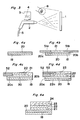
- Figs. 4a to 4e show a process for making superconductive films having a lamination structure to be used for a magnetic sensor.
- the first aqueous solution made as described above is sprayed over a stabilized zirconia substrate 18 having a width of 5 mms and a length of 20 mms which is heated at a temperature in the range from 300°C to 600°C, and thereafter, it is heated at a temperature in the range from 900°C to 1000°C in air at one atmospheric pressure so as to form a superconductive ceramic film 20 of Y1Ba2Cu3O y (6.8 ⁇ y ⁇ 7.0) on the substrate 18 as shown in Fig. 4a.
- each powder is sufficiently dissolved into pure water so as to prepare a second aqueous solution containing Y, Ba, Cu, Zn nitrates.
- the second aqueous solution is sprayed over the top surface of the superconductive ceramic film 20 by the above spray pyrolysis method in such a state that the right and left side portions 20a and 20b of the film 20 are covered by mask films 51a and 51b, respectively, as shown in Fig.
- the first aqueous solution which is made as described above is sprayed over the top surface of the insulation film 21 and the top surface of the left side portion 20b of the superconductive ceramic film 20 by the above spray pyrolysis method in such a state that the right side portion 20a of the superconductive ceramic film 20 is covered by a mask film 52, as shown in Fig. 4c, so as to form a superconductive ceramic film 22 thereon except for the right side portion 20a of the film 20.
- the second aqueous solution which is made as described above is sprayed over the top surface of the superconductive ceramic film 22 by the above spray pyrolysis method in such a state that the right side portion 22a of the superconductive ceramic film 22 is covered by a mask film 53, as shown in Fig. 4d, so as to form an insulation film 23 thereon except for the right side portion 22a of the film 22.
- a superconductive ceramic film 24 is formed in the manner similar to that of the process for making the superconductive ceramic film 22 shown in Fig. 4c.
- the process for forming the superconductive ceramic film and the insulation film is repeated so as to form the superconductive ceramic films having a lamination structure to be used for the magnetic sensor shown in Fig. 5.
- ten superconductive ceramic films 20, 22, 24, 26, 28, 30, 32, 34, 36 and 38 are laminated one by one, and nine electrical insulation films 21, 23, 25, 27, 29, 31, 33, 35 and 37 are formed between the adjacent superconductive ceramic films so as to insulate them except for one end portion of them.
- the insulation film for insulating the upper pair of the adjacent superconductive ceramic films is formed so as to extend in a direction opposite to that of the lower pair of the adjacent films, resulting in that a folded current path is formed in the magnetic sensor shown in Fig. 5.
- respective superconductive ceramic films 20, 22, 24, 26, 28, 30, 32, 34, 36 and 38 which have been made in the above process are electrically connected in series to each other.
- the lattice constant of each superconductive ceramic film is substantially same as that of each insulation film, and the thermal expansion coefficient of each superconductive ceramic film is substantially same as that of each insulation film. Therefore, in the magnetic sensor, any defect due to the mismatching between the lattice does not occur and any peel between the films does not occur, resulting in that there is obtained the superconductive ceramic films having a lamination structure of a good quality to be used for the magnetic sensor.
- a pair of current electrodes 8 and 12 of Ti and a pair of voltage electrodes 9 and 13 of Ti are formed by the vapor deposition method, respectively.
- a pair of current electrodes 8 and 12 is connected to a constant-current regulated power source 16 for supplying a constant current I through lead wires 10 and 15 bonded thereon with use of Ag paste.
- a pair of voltage electrodes 9 and 13 is connected to a voltmeter 17 for measuring a voltage generated in the magnetic sensor through lead wires 11 and 14 bonded thereon with use of Ag paste.
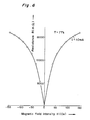
- Fig. 6 is a graph showing the result obtained by measurement with use of the magnetic sensor having laminated ten superconductive ceramic films shown in Fig. 5 which is immersed in liquid nitrogen so as to be cooled at 77K.
- the thickness of each superconductive ceramic film is 10 ⁇ ms, and a current of 1 mA is supplied to the magnetic sensor.
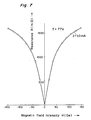
- Fig. 7 is a graph showing the result obtained by measurement with use of a magnetic sensor of a comparative example having one superconductive ceramic film which is made in the manner similar to that of the magnetic sensor of the present preferred embodiment shown in Fig. 5.
- the thickness of the superconductive ceramic film of the magnetic sensor of the comparative example is 10 ⁇ ms, and a current of 1 mA is supplied thereto.
- the magnetic sensor of the preferred embodiment according to the present invention generates ten times the voltage generated by the magnetic sensor of the comparative example having only one superconductive ceramic film, resulting in that the magnetic sensor having a high sensitivity is obtained.
- the superconductive ceramic films of Y1Ba2Cu3O y (6.8 ⁇ y ⁇ 7.0) and the electrical insulation films of Y1Ba2Cu 2.5 Zn 0.5 O y (6.8 ⁇ y ⁇ 7.0) are used, however, superconductive ceramic films of Y1Ba2Cu3O y (6.5 ⁇ y ⁇ 6.8) and electrical insulation films of Y1Ba2Cu 2.5 Zn 0.5 O y (6.5 ⁇ y ⁇ 6.8) may be used.
- the threshold temperature of the superconductive ceramic films of Y1Ba2Cu3O y (6.5 ⁇ y ⁇ 6.8) at which they changes from the normal conductive phase to the superconductive phase are smaller than the threshold temperature of the superconductive ceramic films of Y1Ba2Cu3O y (6.8 ⁇ y ⁇ 7.0).
- the magnetic sensor having the superconductive ceramic films of Y-Ba-Cu-O compounds is described, however, the present invention is not limited to this.
- the spray pyrolysis method is used for forming a superconductive ceramic film, however, the present invention is not limited to this.
- the other methods for forming a superconductive ceramic film such as a spattering method, a CVD method may be used.
- a magnetic sensor comprising the superconductive ceramic films respectively having a smaller thickness has a higher sensitivity, however, when the thickness thereof is equal to or smaller than 0.1 ⁇ ms, a constant magneto-resistive property of the superconductive ceramic film is not obtained because the grains thereof has grown irregularly due to the heating process after forming the superconductive film.
- the thickness of the superconductive ceramic film is equal to or larger than 50 ⁇ ms, the smoothness of the surface thereof and the sensitivity of the magnetic sensor are lowered because the grains of the superconductor has grown excessively.
- the insulation film of Y1Ba2Cu 2.5 Zn 0.5 O y is used for insulating the adjacent superconductive ceramic films, however, the present invention is not limited to this.
- the ratio of composition of elements constituting the ceramic superconductor may be changed so as to form an insulation superconductive ceramic film suitable for making the magnetic sensor comprising the superconductive ceramic films having a lamination structure.
- a material of compounds such as A1Ba2Cu3O y (6.5 ⁇ y ⁇ 7.0) or A1Ba 2-x Sr x Cu3O y (0 ⁇ x ⁇ 0.5, 6.5 ⁇ y ⁇ 7.0) may be used, wherein the above element A is either Lu, Yb, Tm, Er, Y, Ho, Dy, Gd, Eu, Sm or Nd.
- a material of compounds such as Q1Ba2Cu3O y (6.5 ⁇ y ⁇ 7.0), Q1Ba2Cu 3-z M z O y (6.5 ⁇ y ⁇ 7.0, z ⁇ 0.5), Q1Ba 2-x Sr x Cu3O y (x > 0.5, 6.5 ⁇ y ⁇ 7.0), Q1Ba 2-x Sr x Cu 3-z M z O y (x > 0.5, 6.5 ⁇ y ⁇ 7.0, z ⁇ 0.5), Y1Ba2Cu 3-z M z O y (6.5 ⁇ y ⁇ 7.0, z ⁇ 0.5), Y1Ba 2-x Sr x Cu3O y (x > 0.5, 6.5 ⁇ y ⁇ 7.0), Y1Ba 2-x Sr x Cu 3-z M z O y (x > 0.5, 6.5 ⁇ y ⁇ 7.0, Y1Ba 2-x Sr x Cu 3-z M
- each superconductive ceramic film may be shaped into a zigzag configuration as shown in Fig. 8 by using a photolithograph method etc. and an etching method or a masked film deposition method.
- the number of the grain boundaries which are in contact in series can be further increased, resulting in that a magnetic sensor having a higher sensitivity can be obtained.
- the magnetic sensor utilizing the magneto-resistive device constituted by the superconductive ceramic films having a lamination structure according to the present invention which has an extremely high sensitivity and acts at an extremely low consumption power.
Landscapes
- Physics & Mathematics (AREA)
- Chemical & Material Sciences (AREA)
- Engineering & Computer Science (AREA)
- Ceramic Engineering (AREA)
- Condensed Matter Physics & Semiconductors (AREA)
- General Physics & Mathematics (AREA)
- Superconductor Devices And Manufacturing Methods Thereof (AREA)
- Measuring Magnetic Variables (AREA)
Applications Claiming Priority (2)
| Application Number | Priority Date | Filing Date | Title |
|---|---|---|---|
| JP63268586A JPH02114575A (ja) | 1988-10-24 | 1988-10-24 | 超電導積層膜磁気抵抗素子 |
| JP268586/88 | 1988-10-24 |
Publications (3)
| Publication Number | Publication Date |
|---|---|
| EP0366396A2 true EP0366396A2 (de) | 1990-05-02 |
| EP0366396A3 EP0366396A3 (en) | 1990-07-25 |
| EP0366396B1 EP0366396B1 (de) | 1994-06-15 |
Family
ID=17460588
Family Applications (1)
| Application Number | Title | Priority Date | Filing Date |
|---|---|---|---|
| EP89310918A Expired - Lifetime EP0366396B1 (de) | 1988-10-24 | 1989-10-24 | Supraleitende magneto-resistive Einrichtung mit laminierten supraleitenden keramischen Filmen |
Country Status (3)
| Country | Link |
|---|---|
| EP (1) | EP0366396B1 (de) |
| JP (1) | JPH02114575A (de) |
| DE (1) | DE68916170T2 (de) |
Cited By (2)
| Publication number | Priority date | Publication date | Assignee | Title |
|---|---|---|---|---|
| EP0642181A1 (de) * | 1993-09-02 | 1995-03-08 | Commissariat A L'energie Atomique | Magnetoresistive Anordnung und Fühler mit wiederholenden geometrischen Strukturen |
| EP0795914A1 (de) * | 1996-03-12 | 1997-09-17 | International Superconductivity Technology Center | Mehrschicht-Oxidsupraleiter und Oxidsupraleiter-Josephson-Anordnung |
Family Cites Families (1)
| Publication number | Priority date | Publication date | Assignee | Title |
|---|---|---|---|---|
| DE3739412A1 (de) * | 1987-11-20 | 1989-06-29 | Heidelberg Motor Gmbh | Hochstromschalter |
-
1988
- 1988-10-24 JP JP63268586A patent/JPH02114575A/ja active Pending
-
1989
- 1989-10-24 DE DE68916170T patent/DE68916170T2/de not_active Expired - Fee Related
- 1989-10-24 EP EP89310918A patent/EP0366396B1/de not_active Expired - Lifetime
Cited By (4)
| Publication number | Priority date | Publication date | Assignee | Title |
|---|---|---|---|---|
| EP0642181A1 (de) * | 1993-09-02 | 1995-03-08 | Commissariat A L'energie Atomique | Magnetoresistive Anordnung und Fühler mit wiederholenden geometrischen Strukturen |
| FR2709600A1 (fr) * | 1993-09-02 | 1995-03-10 | Commissariat Energie Atomique | Composant et capteur magnétorésistifs à motif géométrique répété. |
| US6075360A (en) * | 1993-09-02 | 2000-06-13 | Commissariat A L'energie Atomique | Magnetoresistive component having a multilayer strip with a geometrical pattern |
| EP0795914A1 (de) * | 1996-03-12 | 1997-09-17 | International Superconductivity Technology Center | Mehrschicht-Oxidsupraleiter und Oxidsupraleiter-Josephson-Anordnung |
Also Published As
| Publication number | Publication date |
|---|---|
| DE68916170D1 (de) | 1994-07-21 |
| EP0366396A3 (en) | 1990-07-25 |
| EP0366396B1 (de) | 1994-06-15 |
| DE68916170T2 (de) | 1995-01-05 |
| JPH02114575A (ja) | 1990-04-26 |
Similar Documents
| Publication | Publication Date | Title |
|---|---|---|
| US5051397A (en) | Joined body of high-temperature oxide superconductor and method of joining oxide superconductors | |
| US6011981A (en) | Oxide superconductor multilayered film and oxide superconductor josephson device | |
| US5719105A (en) | Superconducting element | |
| Kendziora et al. | Single-band model for the temperature-dependent Hall coefficient of high-T c superconductors | |
| JPH07209337A (ja) | 高感度を有する磁気抵抗電流センサ | |
| EP0406862B2 (de) | Gerät für die Anwendung von Supraleitfähigkeit | |
| US5140300A (en) | Superconductive magneto-resistive device comprising laminated superconductive ceramic films | |
| EP0366396B1 (de) | Supraleitende magneto-resistive Einrichtung mit laminierten supraleitenden keramischen Filmen | |
| EP0377359B1 (de) | Oxydisches supraleitendes Material, dessen Herstellungsprozess und Anwendung | |
| Legros-Gledel et al. | Influence of the oxygen content on the critical temperature Tc and the thermopower of Y0. 7Ca0. 3Ba2Cu3Oz | |
| EP0510806B1 (de) | Metalloxidisches Material | |
| US5550101A (en) | Superconducting magnetoresistive element having a plurality of weak-coupling portions and a method of fabricating the same | |
| Srinivasan et al. | Enhancement of thermopower in the high T c superconductor YBa2Cu3O7 and related compounds | |
| RU2598405C1 (ru) | Сверхпроводниковый джозефсоновский прибор с композитной магнитоактивной прослойкой | |
| EP0293836B1 (de) | Methode zur Herstellung einer supraleitenden Dünnschicht | |
| Uher et al. | Experimental evidence for multi-band conduction in highly-doped La-Sr-Cu-O superconductors | |
| Hegde et al. | Epitaxial LaNiO3 thin films: A normal metal barrier for SNS junction | |
| EP0576284A1 (de) | Supraleitendes Material aus Metalloxyd und Verfahren zu seiner Herstellung | |
| EP0482198A1 (de) | Supraleitendes element mit oxydischem supraleiter | |
| US5206214A (en) | Method of preparing thin film of superconductor | |
| US5328892A (en) | Oxide superconductor composition and a process for the production thereof | |
| Orlova et al. | Correlation between the electric-field effect and weak-link type in YBa2Cu3− x Oy and YBa2Cu3− x Oy/Agx high-T c superconducting ceramics | |
| EP0588240B1 (de) | Wismut-enthaltender hochtemperatursupraleitender Oxydwerkstoff und Verfahren zur Herstellung desselben | |
| Jedamzik et al. | GdBa/sub 2/Cu/sub 3/O/sub x/for microwave applications: preparation, properties and devices | |
| US5122503A (en) | Superconducting material and method of producing same |
Legal Events
| Date | Code | Title | Description |
|---|---|---|---|
| PUAI | Public reference made under article 153(3) epc to a published international application that has entered the european phase |
Free format text: ORIGINAL CODE: 0009012 |
|
| AK | Designated contracting states |
Kind code of ref document: A2 Designated state(s): DE FR GB |
|
| PUAL | Search report despatched |
Free format text: ORIGINAL CODE: 0009013 |
|
| AK | Designated contracting states |
Kind code of ref document: A3 Designated state(s): DE FR GB |
|
| 17P | Request for examination filed |
Effective date: 19900817 |
|
| 17Q | First examination report despatched |
Effective date: 19930127 |
|
| GRAA | (expected) grant |
Free format text: ORIGINAL CODE: 0009210 |
|
| AK | Designated contracting states |
Kind code of ref document: B1 Designated state(s): DE FR GB |
|
| REF | Corresponds to: |
Ref document number: 68916170 Country of ref document: DE Date of ref document: 19940721 |
|
| ET | Fr: translation filed | ||
| PLBE | No opposition filed within time limit |
Free format text: ORIGINAL CODE: 0009261 |
|
| STAA | Information on the status of an ep patent application or granted ep patent |
Free format text: STATUS: NO OPPOSITION FILED WITHIN TIME LIMIT |
|
| 26N | No opposition filed | ||
| PGFP | Annual fee paid to national office [announced via postgrant information from national office to epo] |
Ref country code: FR Payment date: 20011010 Year of fee payment: 13 |
|
| PGFP | Annual fee paid to national office [announced via postgrant information from national office to epo] |
Ref country code: GB Payment date: 20011024 Year of fee payment: 13 |
|
| PGFP | Annual fee paid to national office [announced via postgrant information from national office to epo] |
Ref country code: DE Payment date: 20011105 Year of fee payment: 13 |
|
| REG | Reference to a national code |
Ref country code: GB Ref legal event code: IF02 |
|
| PG25 | Lapsed in a contracting state [announced via postgrant information from national office to epo] |
Ref country code: GB Free format text: LAPSE BECAUSE OF NON-PAYMENT OF DUE FEES Effective date: 20021024 |
|
| PG25 | Lapsed in a contracting state [announced via postgrant information from national office to epo] |
Ref country code: DE Free format text: LAPSE BECAUSE OF NON-PAYMENT OF DUE FEES Effective date: 20030501 |
|
| GBPC | Gb: european patent ceased through non-payment of renewal fee |
Effective date: 20021024 |
|
| PG25 | Lapsed in a contracting state [announced via postgrant information from national office to epo] |
Ref country code: FR Free format text: LAPSE BECAUSE OF NON-PAYMENT OF DUE FEES Effective date: 20030630 |
|
| REG | Reference to a national code |
Ref country code: FR Ref legal event code: ST |