EP0366244A1 - Verfahren und Vorrichtung zum Kombinieren eines optischen und elektrischen Kanales in einem Elektronenstrahl-Oszillographen - Google Patents
Verfahren und Vorrichtung zum Kombinieren eines optischen und elektrischen Kanales in einem Elektronenstrahl-Oszillographen Download PDFInfo
- Publication number
- EP0366244A1 EP0366244A1 EP89309105A EP89309105A EP0366244A1 EP 0366244 A1 EP0366244 A1 EP 0366244A1 EP 89309105 A EP89309105 A EP 89309105A EP 89309105 A EP89309105 A EP 89309105A EP 0366244 A1 EP0366244 A1 EP 0366244A1
- Authority
- EP
- European Patent Office
- Prior art keywords
- input
- signal
- electrical
- digital
- output
- Prior art date
- Legal status (The legal status is an assumption and is not a legal conclusion. Google has not performed a legal analysis and makes no representation as to the accuracy of the status listed.)
- Granted
Links
- 230000003287 optical effect Effects 0.000 title claims abstract description 38
- 238000000034 method Methods 0.000 title claims description 3
- 230000008878 coupling Effects 0.000 claims 6
- 238000010168 coupling process Methods 0.000 claims 6
- 238000005859 coupling reaction Methods 0.000 claims 6
- 230000002238 attenuated effect Effects 0.000 abstract description 2
- 238000010586 diagram Methods 0.000 description 1
- 230000000694 effects Effects 0.000 description 1
- 230000035945 sensitivity Effects 0.000 description 1
Images
Classifications
-
- G—PHYSICS
- G01—MEASURING; TESTING
- G01R—MEASURING ELECTRIC VARIABLES; MEASURING MAGNETIC VARIABLES
- G01R13/00—Arrangements for displaying electric variables or waveforms
- G01R13/20—Cathode-ray oscilloscopes
- G01R13/22—Circuits therefor
-
- G—PHYSICS
- G01—MEASURING; TESTING
- G01R—MEASURING ELECTRIC VARIABLES; MEASURING MAGNETIC VARIABLES
- G01R13/00—Arrangements for displaying electric variables or waveforms
- G01R13/20—Cathode-ray oscilloscopes
Definitions
- This invention relates to combining optical channels and electrical channels in an oscilloscope. More particularly, the invention relates to combining the channels in a manner which enables the vertical deflection factor to be set for each channel with a single input attenuation selector switch.
- Oscilloscopes contain an input attenuation selector switch which controls an attenuator section in series with the voltage input. In order to maintain a usable signal, the attenuation factor must be increased as the magnitude of the input voltage increases. A typical progression of attenuation on an oscilloscope is 1, 2, 4, 10, 20, 40, etc.
- Typical optical receivers have a photodiode, a transimpedance amplifier, and one feedback resistor which results in limited dynamic range.
- One manner of improving the dynamic range is to include two or more feedback resistors to change the closed loop transimpedance.
- the feedback resistors are usually in parallel and are selectively switched into the circuit depending on the magnitude of the input photocurrent. Integrating the output of the optical receiver into an oscilloscope, however, would result in a deflection factor which is not constant. Due to varying gain modes, the output voltage of the optical receiver could not be directly used by the vertical amplifier of an oscilloscope. For example, if the optical receiver had gain modes of 3K ohms and 30K ohms, the vertical deflection could be 5mV per division and 50mV per division, respectively, depending upon the magnitude of the input photosignal.
- What is desired is a method and apparatus for combining an optical channel and an electrical channel such that the voltage output of each channel is passed through a common vertical amplifier section and the vertical deflection factor is set by a single input attenuation selector switch.
- an oscilloscope contains an electrical channel and an optical channel in which the vertical deflection factor is set by a single input attenuation selector switch.
- the electrical input is passed through an attenuator.
- the optical input is passed through an input transimpedance amplifier having at least two gain modes and an attenuator.
- the output from the input attenuation selector switch is encoded to form a digital output. This output or the direct output of the selector switch selects an attenuation factor for the electrical channel corresponding to the setting of the input attenuation selector switch.
- the digital output is also decoded by a logic block to generate a gain mode logic signal to switch the gain modes of the input transimpedance amplifier.
- the logic block generates a logic signal to select an appropriate attenuation factor for the optical channel according to the setting of the input attenuation selector switch and the gain mode of the input transimpedance amplifier.
- the attenuated voltage output of each channel is selectively switched and passed to a common vertical amplifier section.
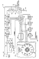
- a combined electrical and optical channel 10 is shown in the SOLE FIGURE as having an optical current input terminal 14 and an electrical voltage input terminal 18.
- the voltage at terminal 18 is passed through attenuators 52, 54, 56, and 58.
- attenuator 52 has an attenuation factor of two and may be disengaged with a digital input signal DB2.
- attenuators 54, 56, and 58 have attenuation factors of four, ten, and one hundred, and may be selectively disengaged with digital input signals DB4, DB10, and DB100, respectively.
- input attenuator switch 16 is used to directly drive the attenuators in the electrical path.
- the output of input attenuation selector switch 16 is then encoded by encoder 38 to form a digital word.
- the exact nature of the logic function and digital circuitry of encoder 38 depends upon the nature of the input attenuator selector switch. Depending upon the nature of selector switch 16, or if desired, the digital word may be used to select appropriate attenuator sections 52, 54, 56, and 58 in accordance with the setting of the input selector switch 16.
- the outputs of the encoder 38 being used to drive the attenuators are shown as dashed lines in the SOLE FIGURE.
- the voltage at the output of attenuator 58 is coupled to the vertical amplifier section through terminal 44.
- the optical channel current input is shown in the SOLE FIGURE at terminal 14.
- the current at terminal 14 is transformed into an output voltage by an input transimpedance amplifier consisting of operational amplifier 20, feedback resistors 34 and 36, and switch 24.
- a transimpedance of 3K ohms or 30K ohms is selected by a digital input to switch 24.
- the output of the transimpedance amplifier is passed to attenuators 26, 28, 30, and 32.
- attenuator 26 has an attenuation factor of 2.5 and may be disengaged with a digital input signal DB2.5.
- Attenuators 28, 30, and 32 have attenuation factors of five, ten, and ten, and may be selectively disengaged with digital input signals DB5, DB10A, and DB10B, respectively.
- the digital word generated by encoder 38 is decoded by logic block 40.
- the logic block generates a gain mode signal labeled GMODE which selects either feedback resistor 34 or 36 depending upon the magnitude of the input photocurrent.
- the logic block 40 generates a digital word which selects appropriate attenuator sections in accordance with the setting of the input selector switch and the gain mode of the input transimpedance amplifier.
- the voltage at the output of attenuator 32 is coupled to the vertical amplifier section through terminal 44.
- logic block 40 enables the single input attenuator selector switch to control the attenuation of the optical channel.
- the following table is constructed by determining the attenuation factors from one setting to the next to achieve constant electrical output sensitivity (e.g., 5mV/Div) for both the electrical and optical channels. It is useful for understanding the nature and design constraints of logic block 40.
- the settings for the input attenuator selector switch are listed in Volts per Division (“Volts/D") for the electrical channel, and Watts per Division (“Watts/D”) for the optical channel.
- An "X" denotes that an attenuator is being used in the circuit.
- RF designates the value of feedback resistor being used in the input transimpedance amplifier.
- logic block 40 is designed such that the attenuation factors for the electrical and optical channels increase by the desired ratios.
- a digital input signal O/E at terminal 12 is used to determine whether the optical signal or the electrical signal will be passed to the vertical amplifier section.
- digital signal O/E engages attenuators 26, 28, 30, and 32 in order that a maximum attenuation is achieved in the optical channel.
- the O/E input is received by a second logic input to the attenuators and engages the attenuators without regard to the value of digital signals DB2.5, DB5, DB10A, and DB10B. Maximum attenuation is desired to minimize crosstalk between the electrical and optical channels.
- Digital signal O/E is also used to open switch 42, and to change the polarity of switch 46, in order that the optical signal is disconnected and that the electrical signal is connected to terminal 44.
- digital signal O/E closes switch 42, and changes the polarity of switch 46, in order that the electrical signal is shorted to ground through 1MEG ohm resistor 48 and crosstalk is reduced, and that the optical signal is routed to terminal 44.
- the attenuators for the electrical and optical channel may be more or less than four in number, and may be of any conventional Pi or T configuration.
- the transimpedance amplifier in the optical channel may have more than two gain modes selectable by switch 24.
- these other embodiments will necessitate a different logic function for logic block 40.
- the design of the logic block will be determined by the analysis of a table showing the attenuation factors in a manner similar to that which is described herein.
Landscapes
- Physics & Mathematics (AREA)
- General Physics & Mathematics (AREA)
- Optical Communication System (AREA)
- Photometry And Measurement Of Optical Pulse Characteristics (AREA)
- Amplifiers (AREA)
Applications Claiming Priority (2)
| Application Number | Priority Date | Filing Date | Title |
|---|---|---|---|
| US07/263,147 US4859935A (en) | 1988-10-27 | 1988-10-27 | Method and apparatus for combining an optical and electrical channel in an oscilloscope |
| US263147 | 1988-10-27 |
Publications (2)
| Publication Number | Publication Date |
|---|---|
| EP0366244A1 true EP0366244A1 (de) | 1990-05-02 |
| EP0366244B1 EP0366244B1 (de) | 1993-11-03 |
Family
ID=23000568
Family Applications (1)
| Application Number | Title | Priority Date | Filing Date |
|---|---|---|---|
| EP89309105A Expired - Lifetime EP0366244B1 (de) | 1988-10-27 | 1989-09-07 | Verfahren und Vorrichtung zum Kombinieren eines optischen und elektrischen Kanales in einem Elektronenstrahl-Oszillographen |
Country Status (3)
| Country | Link |
|---|---|
| US (1) | US4859935A (de) |
| EP (1) | EP0366244B1 (de) |
| JP (1) | JPH0623795B2 (de) |
Cited By (2)
| Publication number | Priority date | Publication date | Assignee | Title |
|---|---|---|---|---|
| US6207183B1 (en) | 1995-12-09 | 2001-03-27 | Lts Lohmann Therapie-Systeme Ag | Surface-stabilized pharmaceutical preparation for application on the skin |
| CN102914700A (zh) * | 2012-09-28 | 2013-02-06 | 西北核技术研究所 | 一种超宽谱脉冲幅值的自校准测量方法 |
Families Citing this family (2)
| Publication number | Priority date | Publication date | Assignee | Title |
|---|---|---|---|---|
| NL9100409A (nl) * | 1991-03-07 | 1992-10-01 | Philips Nv | Meetinstrument voor het meten van weer te geven grootheden en pulsverwerkingsinrichting geschikt voor toepassing in een dergelijk meetinstrument. |
| US5336989A (en) * | 1991-09-19 | 1994-08-09 | Audio Presicion | AC mains test apparatus and method |
Family Cites Families (3)
| Publication number | Priority date | Publication date | Assignee | Title |
|---|---|---|---|---|
| US4553091A (en) * | 1983-02-07 | 1985-11-12 | Tektronix, Inc. | Automatic vertical calibration method and system for an oscilloscope |
| US4654610A (en) * | 1985-07-23 | 1987-03-31 | Hewlett-Packard Company | PIN diode switched RF signal attenuator |
| US4806888A (en) * | 1986-04-14 | 1989-02-21 | Harris Corp. | Monolithic vector modulator/complex weight using all-pass network |
-
1988
- 1988-10-27 US US07/263,147 patent/US4859935A/en not_active Expired - Fee Related
-
1989
- 1989-09-07 EP EP89309105A patent/EP0366244B1/de not_active Expired - Lifetime
- 1989-10-25 JP JP1278330A patent/JPH0623795B2/ja not_active Expired - Lifetime
Non-Patent Citations (4)
| Title |
|---|
| ELECTRONIQUE INDUSTRIELLE, no. 47, February 1983, pages 47-53; J. MONTOIS et al.: "Innover en oscilloscopie impose des améliorations de la technologie micro-électronique" * |
| ELEKTOR, vol. 5, no. 7/8, July/August 1979, pages 7-18; "J. MEIER: "Voltage comparsion on a scope" * |
| MESURES, vol. 52, no. 13, 19th October 1987, pages 22,24, Paris, FR; "Hamamatsu: un oscilloscope pour les signaux optiques" * |
| WIRELESS WORLD, vol. 78, no. 1435, January 1972, pages 19-25; W.T. COCKING: "Dual-trace oscilloscope unit" * |
Cited By (3)
| Publication number | Priority date | Publication date | Assignee | Title |
|---|---|---|---|---|
| US6207183B1 (en) | 1995-12-09 | 2001-03-27 | Lts Lohmann Therapie-Systeme Ag | Surface-stabilized pharmaceutical preparation for application on the skin |
| CN102914700A (zh) * | 2012-09-28 | 2013-02-06 | 西北核技术研究所 | 一种超宽谱脉冲幅值的自校准测量方法 |
| CN102914700B (zh) * | 2012-09-28 | 2015-03-18 | 西北核技术研究所 | 一种超宽谱脉冲幅值的自校准测量方法 |
Also Published As
| Publication number | Publication date |
|---|---|
| JPH0623795B2 (ja) | 1994-03-30 |
| EP0366244B1 (de) | 1993-11-03 |
| JPH02170059A (ja) | 1990-06-29 |
| US4859935A (en) | 1989-08-22 |
Similar Documents
| Publication | Publication Date | Title |
|---|---|---|
| CA1167925A (en) | Calibration apparatus for analog-to-digital converter | |
| US5289191A (en) | Bipolar analog-to-digital conversion apparatus with unipolar current and voltage modes | |
| KR960015211B1 (ko) | 자동 이득 제어 회로를 갖는 아날로그-디지탈 변환 장치 | |
| US4035729A (en) | Audio signal quality indicating circuit | |
| EP0260413B1 (de) | Schaltung zum Kombinieren von Funktionen der Generatoren eines zyklischen redundanten Prüfungskodes und von Pseudo-Zufallszahlengeneratoren | |
| US5351030A (en) | Variable attenuator for attenuating gain of analog signal in accordance with digital signal | |
| EP0118178A1 (de) | Verfahren und Anordnung zum Beseitigen der Nullpunktdrift eines Gleichstromverstärkers | |
| EP0500694A1 (de) | Voll differentieller cmos-leistungsverstärker. | |
| EP0366244A1 (de) | Verfahren und Vorrichtung zum Kombinieren eines optischen und elektrischen Kanales in einem Elektronenstrahl-Oszillographen | |
| US5867063A (en) | Gain distribution circuit | |
| US4764678A (en) | Scintillation camera apparatus including autotuning | |
| EP0410399B1 (de) | Videovorverstärkerschaltung | |
| US3582941A (en) | Nonlinear decoder | |
| EP0901221B1 (de) | Differenzausgangsverstärkeranordnung und Verfahren zur Abstimmung der Ausgangsimpedanz für einen solchen Verstärker | |
| KR0154782B1 (ko) | 저항 어레이를 이용한 선로 등화기 | |
| US4250492A (en) | Non-uniform weighting circuitry | |
| US4207596A (en) | Video special effects with cascaded control logic | |
| US6339356B1 (en) | Variable attenuator | |
| US6920334B1 (en) | Method and apparatus for providing gain control feedback in RF amplifiers | |
| EP0031182B1 (de) | Verstärkeranordnung mit parallel angesteuerten Verstärkerabschnitten | |
| US4987606A (en) | Wide band transmission system with biasing of gain control circuit | |
| EP0499800B1 (de) | Komparator für Raumdiversityempfänger | |
| US5241282A (en) | Wide dynamic range, low power, analog-to-digital receiver | |
| EP0528689B1 (de) | Detektor | |
| EP0214703B1 (de) | Analog-Digitalwandler |
Legal Events
| Date | Code | Title | Description |
|---|---|---|---|
| PUAI | Public reference made under article 153(3) epc to a published international application that has entered the european phase |
Free format text: ORIGINAL CODE: 0009012 |
|
| AK | Designated contracting states |
Kind code of ref document: A1 Designated state(s): GB NL |
|
| 17P | Request for examination filed |
Effective date: 19900928 |
|
| 17Q | First examination report despatched |
Effective date: 19920706 |
|
| GRAA | (expected) grant |
Free format text: ORIGINAL CODE: 0009210 |
|
| AK | Designated contracting states |
Kind code of ref document: B1 Designated state(s): GB NL |
|
| PLBE | No opposition filed within time limit |
Free format text: ORIGINAL CODE: 0009261 |
|
| STAA | Information on the status of an ep patent application or granted ep patent |
Free format text: STATUS: NO OPPOSITION FILED WITHIN TIME LIMIT |
|
| 26N | No opposition filed | ||
| PGFP | Annual fee paid to national office [announced via postgrant information from national office to epo] |
Ref country code: GB Payment date: 19960820 Year of fee payment: 8 |
|
| PGFP | Annual fee paid to national office [announced via postgrant information from national office to epo] |
Ref country code: NL Payment date: 19960830 Year of fee payment: 8 |
|
| PG25 | Lapsed in a contracting state [announced via postgrant information from national office to epo] |
Ref country code: GB Free format text: LAPSE BECAUSE OF NON-PAYMENT OF DUE FEES Effective date: 19970907 |
|
| PG25 | Lapsed in a contracting state [announced via postgrant information from national office to epo] |
Ref country code: NL Free format text: LAPSE BECAUSE OF NON-PAYMENT OF DUE FEES Effective date: 19980401 |
|
| GBPC | Gb: european patent ceased through non-payment of renewal fee |
Effective date: 19970907 |
|
| NLV4 | Nl: lapsed or anulled due to non-payment of the annual fee |
Effective date: 19980401 |