EP0366176A1 - Receiver for use in a remote control system - Google Patents
Receiver for use in a remote control system Download PDFInfo
- Publication number
- EP0366176A1 EP0366176A1 EP89202561A EP89202561A EP0366176A1 EP 0366176 A1 EP0366176 A1 EP 0366176A1 EP 89202561 A EP89202561 A EP 89202561A EP 89202561 A EP89202561 A EP 89202561A EP 0366176 A1 EP0366176 A1 EP 0366176A1
- Authority
- EP
- European Patent Office
- Prior art keywords
- circuit
- receiver
- input
- output
- selective amplifier
- Prior art date
- Legal status (The legal status is an assumption and is not a legal conclusion. Google has not performed a legal analysis and makes no representation as to the accuracy of the status listed.)
- Granted
Links
Images


Classifications
-
- H—ELECTRICITY
- H04—ELECTRIC COMMUNICATION TECHNIQUE
- H04B—TRANSMISSION
- H04B10/00—Transmission systems employing electromagnetic waves other than radio-waves, e.g. infrared, visible or ultraviolet light, or employing corpuscular radiation, e.g. quantum communication
- H04B10/11—Arrangements specific to free-space transmission, i.e. transmission through air or vacuum
- H04B10/114—Indoor or close-range type systems
-
- H—ELECTRICITY
- H04—ELECTRIC COMMUNICATION TECHNIQUE
- H04B—TRANSMISSION
- H04B10/00—Transmission systems employing electromagnetic waves other than radio-waves, e.g. infrared, visible or ultraviolet light, or employing corpuscular radiation, e.g. quantum communication
- H04B10/60—Receivers
Abstract
Description
- The invention generally relates to a remote control system in which pulse sequences which serve as commands are transmitted in the wireless mode after modulation on an appropriate carrier signal to one or a plurality of receivers. The transmitter usually forms part of a hand-held unit controllable by a user whilst the receiver forms part of the apparatus to be controlled, for example an audio set, a video set or as occurs to an ever increasing extent at present, a hearing aid.
- The invention particularly relates to such a receiver.
- In the sequel of this description the remote control system will be abbreviated to RC-systems, the transmitter used therein to RC-transmitter and a receiver to RC-receiver.
- In a remote control system the RC-transmitter includes a message generator which in response to a relevant request by the user supplies a message which consists of a plurality of clock pulse-modulated information pulses. For the transmission of this message to the RC-receiver an infrared modulation circuit is nowadays usually provided, which includes an infrared LED whose radiated infrared light is modulated by the modulated pulses in the pulse train.
- The RC-receiver then includes an infrared photodiode which converts the received infrared light into an electric signal. This signal is applied to a signal processing circuit for generating the original message.
- Embodiments of said RC-transmitters and RC-receivers are extensively described in the reference. The RC-receivers described there comprise a cascade arrangement of an input circuit, a modulation circuit, a pulse shaper and an output circuit. The input circuit receives the output signal of the photodiode and includes an input resonant circuit which is tuned to a frequency which corresponds to the clock pulse frequency (38 kHz here). In addition, this input circuit includes an amplifier circuit in the form of a differential amplifier which amplifies the output signal of the input resonant circuit and applies it to the demodulation circuit. This input circuit acts as a selective amplifier circuit which prevents the proper operation of the RC-receiver from being disturbed by other types of light sources which also transmit infrared light, such as the sun, incandescent lamps etc. So as to still further suppress the disadvantageous influence of these light sources the demodulator circuit is provided with a demodulation resonant circuit which is also tuned to said clock pulse frequency.
- Of this prior art infrared RC-receivers the amplifier circuit, the demodulation circuit, the pulse shaper, the output circuit and a still further number of circuits are jointly designed as one integrated circuit. However, with the object of obtaining the required selectivity, both the input resonant circuit and the demodulation resonant circuit are designed as discrete components, such as capacitors and, more specifically inductances. As a result thereof, the complete RC-receiver is too big to be accommodated in very small housings, such as, for example, in hearing aids. This problem can be obviated to a very high extent by the use of gyrators by means of which these discrete components can be translated to integrable circuitry. This would indeed solve the problem of bulk to a very great extent, but it has an adverse effect on the ever increasing demand for integrated circuits operating at a low voltage in the order of magnitude of 1.2 V. By way of comparison it should be noted that the RC-receiver described in the reference operates as an approximately 5 V supply voltage. For those RC-receivers this is however no problem since they will usually form part of an apparatus which derives its supply voltage from the mains supply.
- The invention has for its object to provide a RC receiver which on the one hand occupies less volume than the prior art RC receiver and in addition requires a lower supply voltage.
- According to the invention
- the input circuit is constituted by a cascade arrangement of a first and a second selective amplifier circuit receiving the output signal from the photo-diode and each having their highest gain factor at a frequency which is equal to the frequency at which the clock pulses occur;
- the demodulation circuit is formed by a mean value detector. - More specifically the first selective amplifier circuit is constituted by an operational amplifier which receives the output signal of the photo-diode via a first filter circuit at a first input, this first input also being connected via a second filter circuit of the operational amplifier, the output further being connected to the second input of the operational amplifier via a first resistance network and this second input being connected to a reference source via a further resistance network.
- Since now the first and second filter circuits both can be assembled from resistors and capacitors, this first selective amplifier circuit can be fully designed in integrated form.
- The second selective amplifier circuit is more specifically formed by an amplifier which now has a finite gain and a first input of which is connected via a capacitance network to the output of the first selective amplifier circuit and via a capacitive network to a reference source. The output of this amplifier is coupled directly to the output of the first selective amplifier circuit and capacitively also to said reference source. The second input of the operational amplifier is directly connected to a further reference source.
- As this second selective amplifier circuit exclusively includes resistors and capacitors in addition to the amplifier, also this second selective amplifier circuit can be fully produced in integrated circuitry.
- The use of said amplifiers in these selective amplifier circuits has the further advantage that the supply voltage can remain low; it need not be more than, for example, approximately 1.2 V.
- Because of the use of the second selective amplifier circuit the demodulation circuit can be in the form of a mean value detector, which detector can also be operated at a supply voltage of approximately 1.2 V. This in contradistinction to the synchronous demodulator used in the RC-receivers described in the reference which require a considerably higher supply voltage (5 Volts).
- Low-power remote control IR transmitter and receiver preamplifiers;
Philips' Electronic Components and Materials;
Technical publication 167 dated 22 March 1985. -
- Fig. 1 is a schematical representation of a message as generated by a RC-transmitter for transmission to a RC-receiver,
- Fig. 2 shows schematically the structure of the RC-receiver according to the invention,
- Fig. 3 shows the current transfer function of the first selective amplifier circuit,
- Fig. 4 shows the impedance-frequency characteristic of the second selective amplifier circuit,
- Fig. 5 shows in detail the structure of the two selective amplifier circuits.
- In Fig. 1 a message is shown schematically at A such as it is to be transmitted from an RC-transmitter to an RC-receiver. This message is assembled in the manner described in the reference and comprises a reference bit REF, a what is commonly referred to as a toggle bit TG, an address word formed by three address bits S0, S1, S2 and a command word formed by six command bits R1, R2, ... R6. The functions of these bits are extensively described in the reference and are not important for a proper understanding of the invention. Each bit consists of two pulses having a length tpw and an interposed pulse pause. The length of this pulse pause determines the logic value of the relevant bit. More specifically, the bit having the logic value "0" is defined by a pulse pause tb0 and a bit having the logic value "1" is defined by a pulse pause tb1. As is customary, these pulse pauses are expressed in numbers of clock pulse periods tosc of a reference clock. Some characteristic values are:
clock frequency of the reference clock fosc = 455 kHz
clock pulse period of the reference clock tosc = 32µs
pulse pause of logic "0" tb0 = 2240 tosc
pulse pause for logic "1" tb1 = 3392 tosc
pulse length tpw = 64 tosc
repetition rate of a message tW = 55296 tosc. - The pulses shown at A for transmission to the RC receiver are first modulated on a carrier of approximately 38 kHz. This results in the signal shown schematically at B in Fig. 1, wherein as will be described in greater detail in Fig. 1 at C each original pulse having pulse length tpw has been replaced by a train of six modulation pulses having a period duration tM = 12 tosc = 26.4µs and a pulse width tMH = 4 tosc = 8 .8 µs. For the ultimate transmission of the message these modulation pulses are modulated on an infrared carrier.
- Fig. 2 shows an embodiment of a RC-receiver suitable for the reception of messages of the format as shown in Fig. 1 at B. This RC-receiver includes a
photodiode 1 which is connected between a +Vb supply voltage 1.3 Volt and ground and through which a current IO flows when it is exposed to infrared light. This current is applied to a firstselective amplifier circuit 2 via an input 2.00. This amplifier circuit supplies from its output 2.01 an output current I₂.₀₁ which in the embodiment shown is converted by a polarity inverting stage 3 into a current -I₂.₀₁ which is applied to a secondselective amplifier circuit 4 via an input 4.01. This amplifier circuit supplies from its output 4.02 a signal which represents a rough version of the pulse train shown at B in Fig. 1 and which is applied to amean value detector 5. This detector supplies a rough version of the original message; i.e. the pulse train shown at A in Fig. 1. This rough version is shaped by the pulse shaper 6 which results in the pulse train shown at A in Fig. 1. In anoutput stage 7 the pulses of the pulse train are adjusted to a value suitable for processing by further circuits. - In the embodiment shown the central section of the first
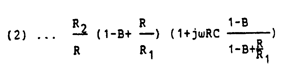
selective amplifier circuit 2 is formed by an operational amplifier 2.02 whose inverting input (-) is connected to the anode of thephotodiode 1 via a cascade arrangement of a resistor 2.03, a capacitor 2.04 and a resistor 2.05. The junction point of resistor 2.05 and capacitor 2.04 is connected to ground potential via a resistor 2.06. The output of the operational amplifier 2.02 is connected to its inverting input (-) via a parallel arrangement of a resistor 2.07 and a capacitor 2.08. This parallel arrangement consequently constitutes a negative feedback. The output of the operational amplifier 2.02 is further connected to ground potential via a series arrangement of two resistors 2.09 and 2.10, the junction point of these two resistors being connected to the non-inverting input (+) of the operational amplifier 2.02. - If the current flowing to capacitor 2.04 is denoted by Ii, the capacitance of each of the capacitors 2.04 and 2.08 is denoted by C, the resistance values of each of the resistors 2.03 and 2.07 by R, the resistance value of resistor 2.06 by R₂ and the resistance values of the resistors 2.09 and 2.10 are denoted by (1-B)R₁ and BR₁, respectively, then it can be written for the voltage gain V₂.₀₁/Vi of this circuit that:

- The relation measured between the absolute value of this current gain on the one hand and ω on the other hand is shown graphically in Fig. 3 for the case in which B = 1/2.
- Since the pulses of the message consist of short pulse trains within which the pulses occur at a rate of 38 kHz, the resonant frequency of this first selective amplifier circuit is chosen to be equal to 38 kHz. This is realised by assigning the following values to the capacitors and resistors
C = 44 pF
R = 100 kΩ
B = ½
R₁ = 200 kΩ" - The central section of the second
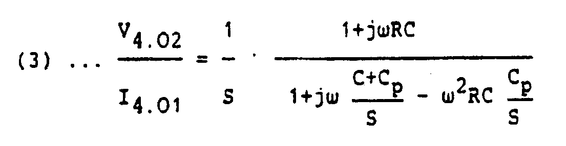
selective amplifier circuit 4 is formed by an amplifier 4.03 having a finite gain factor, or, which is the same, with finite slope S. As is known, the slope of an amplifier is the ratio between its output current and its input current. More specifically the output current -I₂.₀₁ of the polarity inverting stage 3 is applied to the inverting input (-) of amplifier 4.03 via a resistor 4.04 and also to its output via a conductor 4.05. The inverting input (-) is further connected to ground potential via a capacitor 4.06 and the output is connected to ground potential via a capacitor 4.07. The non-inverting input (+) of amplifier 4.03 receives a reference voltage Vref. - If now the voltage at the output 4.02 of this second selective amplifier circuit is denoted by V4.02′ the current applied to its input 4.01 by I₄.₀₁ (= -I₂.₀₁), the resistance value of resistor 4.04 by R₄, the capacitances of capacitors 4.06 and 4.07 by C and Cp, respectively, then it holds that:
- The relation measured between the absolute value of the ratio V₄.₀₂/I₄.₀₁ and ω is shown graphically in Fig. 4.
- The resonant frequency of this second selective amplifier circuit is also chosen to be 38 kHz.
- Because of the special structure of the first selective amplifier circuit it is achieved that at relatively large deviations (of, for example 12 kHz) of the resonant frequency not more than approximately 2 dB of additional gain loss occur. This is a very advantageous property of the selective amplifier circuit as in IC's the RC-product may evidence a spread of up to 32% caused by normal variations, which spread now does not result in a gain loss of more than 2 dB.
- The integrable structure of the first and second
selective amplifier circuit selective amplifier circuit 2 the operational amplifier (2.02) is formed by the transistors 2.11, 2.12, 2.28 and 2.29. The base of transistor 2.11 forms the inverting input (-) of this operational amplifier and the base of transistor 2.12 forms the non-inverting input (+). The emitters of these transistors are connected to a current source circuit formed by the transistors 2.13 and 2.14 which together with a further transistor 2.15 form a current mirror circuit which receives a 0. 8 µA current I₃ from an external source. The base of transistor 2.11 (that is to say the inverting input of the operational amplifier) is connected via resistor 2.03, capacitor 2.04 and resistor 2.05 to the input 2.00 to which the photodiode is connected. The junction point of capacitor 2.04 and resistor 2.05 is connected to ground potential via resistor 2.06. The base of transistor 2.11 is also connected via the parallel arrangement of the resistor 2.07 and capacitor 2.08 to the collector of transistor 2.28 (being the non-inverting output of the operational amplifier). The collector of transistor 2.28 is further connected by means of resistor 2.09 to the base of transistor 2.12 (being the non-inverting input (+) of the operational amplifier). This base is additionally connected via resistor 2.10 to an input to which an external 800 mV reference voltage source Vref is connected. The collector of transistor 2.11 receives a supply voltage Vb of approximately I V from an external voltage source. A current source constituted by a current mirror circuit formed by the transistor 2.20, 2.21, 2.22 is incorporated in the collector of transistor 2.12. This current mirror circuit itself is connected to a further current mirror circuit formed by the transistors 2.23, 2.24, 2.25 and 2.26 which receives a current I₄ of also approximately 0.8 µA from an external source. The collector of transistor 2.12 is connected to the base of a transistor 2.28 which is arranged between the transistors 2.22 and 2.25. The inverting output of this first selective amplifier circuit is formed by the collector of a transistor 2.29 whose base is connected in the manner shown to one of the poles of resistor 2.10 and whose emitter is connected to the current sources 2.25 and 2.26. - The polarity inverting circuit 3 which in this embodiment is constituted by a current mirror circuit formed by the transistors 3.01 and 3.02 is connected to the collector of this transistor 2.29.
- The second
selective amplifier circuit 4 includes the amplifier (4.03) which is comprised of the transistors 4.08 and 4.09. The emitter of these transistors 2.08 and 2.09 are connected to a current source circuit formed by the two transistors 4.10 and 4.11 which together with the transistors 2.26, 2.25, 2.24 and 2.23 form part of a current mirror circuit. The collector current of transistor 4.08 is first mirror-inverted by a current mirror circuit comprised of the transistors 4.14 and 4.15 and thereafter once again by a current mirror circuit comprised of the transistor 4.12 and 4.13 and is thereafter subtracted from the current supplied by the current mirror circuit 3.01, 3.02. The circuit adjusts itself such that the d.c. voltage at the base of 4.08 becomes accurately equal to the voltage at the base of transistor 4.09 (Vref). As a result thereof the d.c. voltage at the input 4.01 of this second selective amplifier circuit becomes some mV higher than Vref. The inverting input (-) of this amplifier is constituted by the base of transistor 4.08 and is connected via the resistor 4.04 to the output of the current mirror circuit (3.01, 3.02) and also via the capacitor 4.06 to ground potential. The non-inverting input also receives said reference voltage Vref. Finally, the output of this second selective amplifier circuit is formed by the collector of transistor 4.12 whose parasitic capacitance performs the function of the capacitor 4.07, together with the capacitance of a capacitor 4.16 which is connected between the collector of transistor 4.12 and ground.
Claims (4)
- the input circuit is constituted by a cascade arrangement of a first and a second selective amplifier circuit each having their highest gain factor at a frequency which is approximately equal to the clock pulse frequency;
- the demodulation circuit is formed by a mean value detector.
Priority Applications (1)
| Application Number | Priority Date | Filing Date | Title |
|---|---|---|---|
| AT89202561T ATE101463T1 (en) | 1988-10-17 | 1989-10-11 | RECEIVER FOR USE IN A REMOTE CONTROL SYSTEM. |
Applications Claiming Priority (2)
| Application Number | Priority Date | Filing Date | Title |
|---|---|---|---|
| NL8802544 | 1988-10-17 | ||
| NL8802544A NL8802544A (en) | 1988-10-17 | 1988-10-17 | RECEIVER FOR APPLICATION IN A REMOTE CONTROL SYSTEM. |
Publications (2)
| Publication Number | Publication Date |
|---|---|
| EP0366176A1 true EP0366176A1 (en) | 1990-05-02 |
| EP0366176B1 EP0366176B1 (en) | 1994-02-09 |
Family
ID=19853067
Family Applications (1)
| Application Number | Title | Priority Date | Filing Date |
|---|---|---|---|
| EP89202561A Expired - Lifetime EP0366176B1 (en) | 1988-10-17 | 1989-10-11 | Receiver for use in a remote control system |
Country Status (7)
| Country | Link |
|---|---|
| US (1) | US5031196A (en) |
| EP (1) | EP0366176B1 (en) |
| JP (1) | JP2911004B2 (en) |
| AT (1) | ATE101463T1 (en) |
| DE (1) | DE68913002T2 (en) |
| DK (1) | DK172624B1 (en) |
| NL (1) | NL8802544A (en) |
Cited By (1)
| Publication number | Priority date | Publication date | Assignee | Title |
|---|---|---|---|---|
| SG93790A1 (en) * | 1993-06-18 | 2003-01-21 | Sony Corp | Wireless receiving apparatus |
Families Citing this family (7)
| Publication number | Priority date | Publication date | Assignee | Title |
|---|---|---|---|---|
| US5243626A (en) * | 1991-08-29 | 1993-09-07 | Apple Computer, Inc. | Method for clocks synchronization for receiving pulse position encoded signals |
| JP2820138B2 (en) * | 1996-11-26 | 1998-11-05 | 日本電気株式会社 | Light modulator |
| AU6419598A (en) * | 1998-03-19 | 1999-10-11 | Hitachi Device Engineering, Co., Ltd. | Optical receiver using variable negative-capacitance circuit |
| US6330091B1 (en) * | 1998-05-15 | 2001-12-11 | Universal Electronics Inc. | IR receiver using IR transmitting diode |
| JP2006339913A (en) * | 2005-05-31 | 2006-12-14 | Sharp Corp | Infrared remote control receiver unit |
| JP3958339B2 (en) * | 2006-01-13 | 2007-08-15 | Smk株式会社 | Pulse modulation method |
| US9246601B2 (en) * | 2011-05-03 | 2016-01-26 | Yunzhi Dong | Optical receiver |
Citations (1)
| Publication number | Priority date | Publication date | Assignee | Title |
|---|---|---|---|---|
| DE3136629A1 (en) * | 1981-09-15 | 1983-04-07 | Loewe Opta Gmbh, 8640 Kronach | Pre-amplifier for an infrared remote control receiver for receiving remote control signals which are pulse-code modulated onto an RF carrier frequency |
Family Cites Families (7)
| Publication number | Priority date | Publication date | Assignee | Title |
|---|---|---|---|---|
| US4317232A (en) * | 1979-01-12 | 1982-02-23 | Deere & Company | Fiber optic signal conditioning circuit |
| US4426662A (en) * | 1982-01-18 | 1984-01-17 | Zenith Radio Corporation | IR Remote control detector/decoder |
| US4489420A (en) * | 1983-03-09 | 1984-12-18 | General Electric Company | Clear channel detector for binary digital data transmission system |
| US4718119A (en) * | 1984-08-27 | 1988-01-05 | Motorola Inc. | AGC circuit including a precision voltage clamp and method |
| US4713841A (en) * | 1985-06-03 | 1987-12-15 | Itt Electro Optical Products, A Division Of Itt Corporation | Synchronous, asynchronous, data rate transparent fiber optic communications link |
| US4821338A (en) * | 1985-08-07 | 1989-04-11 | Minolta Camera Kabushiki Kaisha | Optical signal receiving apparatus with compensation for peripheral light |
| US4817208A (en) * | 1987-09-08 | 1989-03-28 | Westinghouse Electric Corp. | Fiber optic receiver |
-
1988
- 1988-10-17 NL NL8802544A patent/NL8802544A/en not_active Application Discontinuation
-
1989
- 1989-09-29 US US07/414,566 patent/US5031196A/en not_active Expired - Fee Related
- 1989-10-11 EP EP89202561A patent/EP0366176B1/en not_active Expired - Lifetime
- 1989-10-11 DE DE68913002T patent/DE68913002T2/en not_active Expired - Fee Related
- 1989-10-11 AT AT89202561T patent/ATE101463T1/en not_active IP Right Cessation
- 1989-10-13 DK DK198905084A patent/DK172624B1/en not_active IP Right Cessation
- 1989-10-16 JP JP1266364A patent/JP2911004B2/en not_active Expired - Lifetime
Patent Citations (1)
| Publication number | Priority date | Publication date | Assignee | Title |
|---|---|---|---|---|
| DE3136629A1 (en) * | 1981-09-15 | 1983-04-07 | Loewe Opta Gmbh, 8640 Kronach | Pre-amplifier for an infrared remote control receiver for receiving remote control signals which are pulse-code modulated onto an RF carrier frequency |
Non-Patent Citations (2)
| Title |
|---|
| ELEKTROTECHNIK, vol. 63, no. 19, 10/1981, Würzburg, DE, page 71; "Vorverstärker für Infrarotempfänger" * |
| IEEE JOURNAL OF LIGHTWAVE TECHNOLOGY, vol. LT-3, no. 1, 2/1985, New York, US; M.J.N. SIBLEY et al.: "A monolithic common-collector front-end optical preamplifier", pages 13-15 * |
Cited By (1)
| Publication number | Priority date | Publication date | Assignee | Title |
|---|---|---|---|---|
| SG93790A1 (en) * | 1993-06-18 | 2003-01-21 | Sony Corp | Wireless receiving apparatus |
Also Published As
| Publication number | Publication date |
|---|---|
| US5031196A (en) | 1991-07-09 |
| EP0366176B1 (en) | 1994-02-09 |
| JPH02150195A (en) | 1990-06-08 |
| JP2911004B2 (en) | 1999-06-23 |
| DK172624B1 (en) | 1999-03-08 |
| DE68913002D1 (en) | 1994-03-24 |
| NL8802544A (en) | 1990-05-16 |
| DK508489A (en) | 1990-04-18 |
| DE68913002T2 (en) | 1994-08-04 |
| DK508489D0 (en) | 1989-10-13 |
| ATE101463T1 (en) | 1994-02-15 |
Similar Documents
| Publication | Publication Date | Title |
|---|---|---|
| JP3350376B2 (en) | Waveform shaping circuit and infrared data communication device using the same | |
| KR100400224B1 (en) | Burst mode receiving apparatus having function for compensating offset and data recovery method thereof | |
| EP0366176B1 (en) | Receiver for use in a remote control system | |
| US4817208A (en) | Fiber optic receiver | |
| US7355456B2 (en) | Wide linear range peak detector | |
| US6100764A (en) | Remote control preamp circuit | |
| KR960014410B1 (en) | Infrared ray receiving circuit | |
| US5712475A (en) | Light receiving circuit with variable threshold circuit | |
| JP3214196B2 (en) | Light receiving circuit for AV optical space transmission | |
| EP0367333A1 (en) | Remote-controlled receiver with resupply of energy to battery | |
| JP3181458B2 (en) | Gain switching type optical receiving amplifier | |
| JP2002124857A (en) | Signal compensation circuit and demodulation circuit | |
| JPH01286655A (en) | Light receiving circuit | |
| EP0202601A2 (en) | Optical pulse receiving circuit | |
| JPH10215270A (en) | Communication equipment for vehicle | |
| JP2006115343A (en) | Waveform forming device | |
| JP3470887B2 (en) | Photoelectric conversion circuit | |
| JP2001007684A (en) | Remote control receiver and disturbing wave eliminating method | |
| JP3088138B2 (en) | Detection circuit | |
| JP2000357957A (en) | Light receiving circuit and optical transmitter using the circuit | |
| JPH0449739A (en) | Optical receiver | |
| JP2001203640A (en) | Receiver, symbol restoration system and information restoration method | |
| JPH08307358A (en) | Photodetector | |
| JPH021634A (en) | Light-receiving circuit | |
| JPH1098337A (en) | Amplifier |
Legal Events
| Date | Code | Title | Description |
|---|---|---|---|
| PUAI | Public reference made under article 153(3) epc to a published international application that has entered the european phase |
Free format text: ORIGINAL CODE: 0009012 |
|
| AK | Designated contracting states |
Kind code of ref document: A1 Designated state(s): AT CH DE FR GB IT LI |
|
| 17P | Request for examination filed |
Effective date: 19901031 |
|
| 17Q | First examination report despatched |
Effective date: 19921102 |
|
| GRAA | (expected) grant |
Free format text: ORIGINAL CODE: 0009210 |
|
| AK | Designated contracting states |
Kind code of ref document: B1 Designated state(s): AT CH DE FR GB IT LI |
|
| REF | Corresponds to: |
Ref document number: 101463 Country of ref document: AT Date of ref document: 19940215 Kind code of ref document: T |
|
| REF | Corresponds to: |
Ref document number: 68913002 Country of ref document: DE Date of ref document: 19940324 |
|
| ITF | It: translation for a ep patent filed |
Owner name: ING. C. GREGORJ S.P.A. |
|
| ET | Fr: translation filed | ||
| PLBE | No opposition filed within time limit |
Free format text: ORIGINAL CODE: 0009261 |
|
| STAA | Information on the status of an ep patent application or granted ep patent |
Free format text: STATUS: NO OPPOSITION FILED WITHIN TIME LIMIT |
|
| 26N | No opposition filed | ||
| ITPR | It: changes in ownership of a european patent |
Owner name: CAMBIO RAGIONE SOCIALE;PHILIPS ELECTRONICS N.V. |
|
| REG | Reference to a national code |
Ref country code: CH Ref legal event code: PFA Free format text: PHILIPS ELECTRONICS N.V. |
|
| REG | Reference to a national code |
Ref country code: FR Ref legal event code: CD |
|
| REG | Reference to a national code |
Ref country code: CH Ref legal event code: PFA Free format text: PHILIPS ELECTRONICS N.V. TRANSFER- KONINKLIJKE PHILIPS ELECTRONICS N.V. |
|
| REG | Reference to a national code |
Ref country code: FR Ref legal event code: CD |
|
| PGFP | Annual fee paid to national office [announced via postgrant information from national office to epo] |
Ref country code: AT Payment date: 20011023 Year of fee payment: 13 |
|
| PGFP | Annual fee paid to national office [announced via postgrant information from national office to epo] |
Ref country code: FR Payment date: 20011026 Year of fee payment: 13 |
|
| PGFP | Annual fee paid to national office [announced via postgrant information from national office to epo] |
Ref country code: GB Payment date: 20011031 Year of fee payment: 13 |
|
| PGFP | Annual fee paid to national office [announced via postgrant information from national office to epo] |
Ref country code: DE Payment date: 20011215 Year of fee payment: 13 |
|
| REG | Reference to a national code |
Ref country code: GB Ref legal event code: IF02 |
|
| PGFP | Annual fee paid to national office [announced via postgrant information from national office to epo] |
Ref country code: CH Payment date: 20020108 Year of fee payment: 13 |
|
| PG25 | Lapsed in a contracting state [announced via postgrant information from national office to epo] |
Ref country code: GB Free format text: LAPSE BECAUSE OF NON-PAYMENT OF DUE FEES Effective date: 20021011 Ref country code: AT Free format text: LAPSE BECAUSE OF NON-PAYMENT OF DUE FEES Effective date: 20021011 |
|
| PG25 | Lapsed in a contracting state [announced via postgrant information from national office to epo] |
Ref country code: LI Free format text: LAPSE BECAUSE OF THE APPLICANT RENOUNCES Effective date: 20021031 Ref country code: CH Free format text: LAPSE BECAUSE OF THE APPLICANT RENOUNCES Effective date: 20021031 |
|
| REG | Reference to a national code |
Ref country code: CH Ref legal event code: PL |
|
| PG25 | Lapsed in a contracting state [announced via postgrant information from national office to epo] |
Ref country code: DE Free format text: LAPSE BECAUSE OF NON-PAYMENT OF DUE FEES Effective date: 20030501 |
|
| GBPC | Gb: european patent ceased through non-payment of renewal fee |
Effective date: 20021011 |
|
| PG25 | Lapsed in a contracting state [announced via postgrant information from national office to epo] |
Ref country code: FR Free format text: LAPSE BECAUSE OF NON-PAYMENT OF DUE FEES Effective date: 20030630 |
|
| REG | Reference to a national code |
Ref country code: FR Ref legal event code: ST |
|
| PG25 | Lapsed in a contracting state [announced via postgrant information from national office to epo] |
Ref country code: IT Free format text: LAPSE BECAUSE OF NON-PAYMENT OF DUE FEES;WARNING: LAPSES OF ITALIAN PATENTS WITH EFFECTIVE DATE BEFORE 2007 MAY HAVE OCCURRED AT ANY TIME BEFORE 2007. THE CORRECT EFFECTIVE DATE MAY BE DIFFERENT FROM THE ONE RECORDED. Effective date: 20051011 |