EP0364700A2 - Bus-coupling circuit - Google Patents
Bus-coupling circuit Download PDFInfo
- Publication number
- EP0364700A2 EP0364700A2 EP89115672A EP89115672A EP0364700A2 EP 0364700 A2 EP0364700 A2 EP 0364700A2 EP 89115672 A EP89115672 A EP 89115672A EP 89115672 A EP89115672 A EP 89115672A EP 0364700 A2 EP0364700 A2 EP 0364700A2
- Authority
- EP
- European Patent Office
- Prior art keywords
- bus
- driver
- voltage
- hysteresis
- arrangement according
- Prior art date
- Legal status (The legal status is an assumption and is not a legal conclusion. Google has not performed a legal analysis and makes no representation as to the accuracy of the status listed.)
- Granted
Links
Images


Classifications
-
- H—ELECTRICITY
- H04—ELECTRIC COMMUNICATION TECHNIQUE
- H04L—TRANSMISSION OF DIGITAL INFORMATION, e.g. TELEGRAPHIC COMMUNICATION
- H04L12/00—Data switching networks
- H04L12/28—Data switching networks characterised by path configuration, e.g. LAN [Local Area Networks] or WAN [Wide Area Networks]
- H04L12/40—Bus networks
- H04L12/40006—Architecture of a communication node
- H04L12/40032—Details regarding a bus interface enhancer
-
- H—ELECTRICITY
- H04—ELECTRIC COMMUNICATION TECHNIQUE
- H04L—TRANSMISSION OF DIGITAL INFORMATION, e.g. TELEGRAPHIC COMMUNICATION
- H04L12/00—Data switching networks
- H04L12/02—Details
- H04L12/10—Current supply arrangements
Definitions
- the invention relates to a bus coupling circuit based on the preamble of patent claim 1.
- Such a bus coupling circuit is known from "Control engineering practice, 25th year, 1983, number 10, pages S61 to S64, and number 10, pages S69 and S70".
- a bus receiver has a hysteresis for suppressing superimposed interference signals.
- Participants e.g. Data transmitters or data receivers, which are connected to one another via a common bus, have driver circuits as interfaces. In the event of a short-circuit in a subscriber or in an interface, the entire bus is often unusable.
- an interface arrangement constructed with optocouplers is known which, in the event of faults in the optocouplers, e.g. in the event of short circuits, a control circuit assigned to the optocouplers prevents the connection between driver and data input from being blocked.
- the object of the invention is to design the bus coupling circuit according to the preamble of patent claim 1 such that bidirectional operation with high data rates is possible even when component failures, in particular short circuits, occur.
- the DC voltage value lost due to the galvanic isolation is restored without distortion by an additional hysteresis circuit. This allows operation with high data rates, since only edges of the data signal have to be evaluated.
- a component in the hysteresis circuit is dimensioned so that bidirectional bus operation is still possible even in the event of short circuits.
- the arrangement according to the invention allows bidirectional data transmission with electrical fault tolerance of several, for example eight, short circuits. Other errors, such as participants marked by mere failure, are negligible for the bus.
- the bus system does not require any clock lines for "bus handling", which further increases reliability. It is also insensitive to incorrect control, since the series resistors, as components of the DC isolating means, also act as protective impedances. An accidentally "clamped” on the bus Driver output (transmission mode) has the same non-disadvantageous effect on the bus as the short circuit of a driver output since static signals are not present on the bus and the DC value is recovered from the edges of the data by artificial hysteresis.
- the configurations according to patent claims 4, 5 and 7 and patent claim 10 have the following additional advantages:
- the signal shape of the digital signals transmitted by the bus improves especially at bit rates> 20 Mbit / s without significantly narrowing the fault tolerance. If the boundary conditions are otherwise the same, more short circuits can be permitted than with the arrangement according to the main application.
- the measures of the invention give the bus an amplitude-dependent passive dynamic termination or an active bus termination (claim 10).
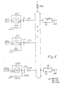
- the bus shown in the figure can be connected via a total of 28 bidirectional drivers T1, T2, ... to the subscribers Tl1, Tl2 ..., eg microprocessors.
- the AC 245 integrated circuits of FACT (Fairchild Advanced CMOS Technology) technology are suitable as bidirectional drivers. Two drivers, one representing a data transmitter and the other a data receiver or vice versa, can be switched in real time in a fault-tolerant manner in groups (8 bits) via these drivers. A short circuit or an interruption in a participant must not have any serious effects on the overall system.
- the driver inputs E21, E22 ... close to the bus are connected to the bus via DC voltage isolating means, each consisting of a series connection of a capacitor C1, C2, ...
- the divider chain ie the series connection of the voltage divider resistors, lies between the input E11 or E12, ... of the driver remote from the bus and half the supply voltage - + 2.5 V for the integrated drivers used.
- the threshold reference voltage of the drivers is thus newly available (dashed line in FIG. 1).
- the divider tap is connected to the driver input E21 or E22, ... near the bus.
- a bus earth resistance R4 of approximately 100 KOhm is provided.
- the hysteresis determines the sensitivity of the receiver around the threshold (at FACT 2.5 volts). It specifies the minimum amplitude (reduction due to short circuits) the system stops functioning, or: how many short circuits the system can ultimately cope with. This situation is explained on the basis of the "steady state": If, for example, a positive edge has occurred on the bus, the AC245 is consequently driven to HIGH via resistor R11 or R12 and capacitor C1 or C2 . It is now connected to the bus with the input side.
- a short circuit for example of a driver output, results in a loss of amplitude.
- VCC positive supply potential
- a short circuit of just one driver to GND is assumed: Then the potential would be set to zero without additional measures.
- the dynamic amplitude would be halved (by the resistance of both the transmitter and the receiver), but limited in its maximum value to + 2.5 volts. But that is exactly the threshold, so that no defined state "HIGH" could be transmitted.
- the basic idea now is to remove this distortion of the DC voltage value by taking additional measures. For this purpose, a sufficiently large capacitor C1 or C2, ...
- resistors R2 and R3 have been assumed to be substantially larger than the series resistors in their entire parallel connection along the bus line.
- the current consumption of the bus drivers used is almost exclusively determined by the external wiring.
- the interface arrangement presented is ideally suited for use in MOBS (modular onboard switching) systems in satellites, especially since faults in resistors are almost always only manifested by an interruption and even short circuits in the series capacitors only have a negative effect if the associated driver is also involved fails due to short circuit. However, this case occurs with a very low probability of association.
- the DC voltage isolation can also be carried out differently than previously described, for example by a transformer U1, U2, ... (FIG. 2). Its secondary winding w2 can be connected directly to the bus, for example.
- the primary winding w1 (of the transformer U1) is connected with its one connection end to the driver input E21 and with its other connection end to the divider tap of the voltage divider consisting of the resistors R21, R31, or R22, R32.
- the voltage divider resistors For the dimensioning of the voltage divider resistors, it must be assumed that on the one hand they must be so high-resistance that the short circuit of a driver is not transformed to the bus as a short circuit or too low impedance, but on the other hand it must also be so low-resistance that a driver has enough power in the direction of transmission can transform to the bus in order to control all other drivers operated as receivers via their assigned transmitters. In real cases, not all of the driver power is transferred to the bus due to leakage losses from the transformers. These requirements are met if the AC parallel impedance of the resistors R2 and R3 is in the order of 100 ohms.
- a high-frequency ferrite core transformer is preferably suitable as the transformer Ü.
- the implementation by means of a transformer as a DC voltage isolation means requires fewer components than the solution presented above with a DC voltage isolation capacitor.
- the probability of failure of the high-frequency ferrite core transformers can be reduced by special construction measures (casting, winding arrangement with a large winding spacing).
- the bus is "open" for signal amplitudes on the bus less than 0.7 V; ie only the ohmic bus ground resistance R4 is effective. If the signal amplitudes on the bus rise above U S , the excess amplitude components are cut off at ⁇ 0.7 V. If a short circuit now occurs, for example at a bus driver output, the bus is additionally loaded in terms of AC voltage with the corresponding resistor R11 ... R128, at whose driver the short circuit occurs. This reduces the signal amplitudes on the bus. The corresponding resistor R11 ... R128 then takes over the bus termination.
- the signal amplitudes on the bus which were previously sufficient to control the diodes D1, D2, D3 and D4, can drop to such an extent that the threshold value U S no longer reaches due to the load with one of the resistors R11 ... becomes.
- the threshold value U S is reached despite additional loading by one of the resistors R11 ... R128, and what is known as a voltage divider behavior occurs:
- the bus is then terminated both with the corresponding resistor R11 ... R128 and with the path resistance of the diodes D1, D2, D3 and D4.
- the resistor R4 is several orders of magnitude larger than the resistors R11 ...
- capacitors CB1 and CB2 must be chosen so large in terms of capacity that the DC voltage value for the hysteresis circuits can still be regenerated from the edges of the transferable data. It is best to choose capacitors CB1 and CB2 each as large as capacitors C1 to C28.
- FIG. 4 Such an exemplary embodiment for a one-sided bus termination is shown in FIG. 4. Here two series parallel connections of diodes are arranged antiparallel to each other.
- the corresponding DC isolating capacitor consists of four partial capacitors - two capacitors connected in series, which are combined to form a parallel connection.
- care must be taken to ensure that the corresponding threshold value U S and the total capacitance CB1 and CB2 are matched to the bus and the other components.
Abstract
Description
Die Erfindung betrifft eine Buskoppelschaltung ausgehend vom Oberbegriff des Patentanspruchs 1.The invention relates to a bus coupling circuit based on the preamble of
Eine solche Buskoppelschaltung ist aus "Regelungstechnische Praxis, 25. Jahrgang, 1983, Heft 10, Seiten S61 bis S64, sowie Heft 10, Seiten S69 und S70" bekannt. Bei der dortigen Buskoppelschaltung weist ein Busempfänger eine Hysterese zur Unterdrückung überlagerter Störsignale auf.Such a bus coupling circuit is known from "Control engineering practice, 25th year, 1983, number 10, pages S61 to S64, and number 10, pages S69 and S70". In the bus coupling circuit there, a bus receiver has a hysteresis for suppressing superimposed interference signals.
Teilnehmer, z.B. Datensender oder Datenempfänger, die über einen gemeinsamen Bus miteinander in Verbindung stehen, weisen als Schnittstelle Treiberschaltungen auf. Bei einem Kurzschluß bei einem Teilnehmer oder in einer Schnittstelle ist oft der gesamte Bus unbrauchbar. Aus der DE 34 33 150 A1 ist eine mit Optokopplern aufgebaute Schnittstellenanordnung bekannt, die bei Fehlern an den Optokopplern, z.B. bei Kurzschlüssen, mittels einer den Optokopplern zugeordneten Kontrollschaltung eine Sperrung der Verbindung zwischen Treiber und Dateneingang verhindert.Participants, e.g. Data transmitters or data receivers, which are connected to one another via a common bus, have driver circuits as interfaces. In the event of a short-circuit in a subscriber or in an interface, the entire bus is often unusable. From DE 34 33 150 A1 an interface arrangement constructed with optocouplers is known which, in the event of faults in the optocouplers, e.g. in the event of short circuits, a control circuit assigned to the optocouplers prevents the connection between driver and data input from being blocked.
Aufgabe der Erfindung ist es, die Buskoppelschaltung gemäß dem Oberbegriff des Patentanspruchs 1 so auszubilden, daß auch beim Auftreten von Bauelementeausfällen, insbesondere Kurzschlüssen, ein bidirektionaler Betrieb mit hohen Datenraten möglich ist.The object of the invention is to design the bus coupling circuit according to the preamble of
Diese Aufgabe wird durch die kennzeichnenden Merkmale des Patentanspruchs 1 gelöst. Die Unteransprüche zeigen vorteilhafte Weiterbildungen auf.This object is achieved by the characterizing features of
Bei der Realisierung gemäß DE 34 33 150 A1 erfolgt bei falscher Ansteuerung z.B. durch einen defekten Teilnehmer - Mikroprozessor - eine Sperrung des Optokopplers mitsamt Treiber. Wenn jedoch der Treiber oder der Optokoppler selbst einen Kurzschluß aufweist, kann der gesamte Bus blockiert werden. Bei der Realisierung gemäß der Erfindung tritt dieser Nachteil nicht auf. Auch ist die Realisierung gemäß DE 34 33 150 A1 nicht für hohe Datenraten brauchbar. Die Realisierung gemäß der Erfindung erfordert wenig Schaltmittel. Es sind lediglich ein als integrierter Baustein erhältlicher bidirektionaler Treiber, drei Widerstände und ein Kondensator pro Teilnehmer notwendig.In the implementation according to DE 34 33 150 A1, incorrect control e.g. due to a defective participant - microprocessor - the optocoupler and driver are blocked. However, if the driver or optocoupler itself is shorted, the entire bus can be blocked. This disadvantage does not occur in the implementation according to the invention. The implementation according to DE 34 33 150 A1 cannot be used for high data rates. The implementation according to the invention requires little switching means. Only one bidirectional driver available as an integrated module, three resistors and one capacitor per subscriber are required.
Bei der Erfindung wird der durch die galvanische Trennung verlorengegangene Gleichspannungswert durch eine zusätzliche Hysteresebeschaltung verzerrungsfrei wiederhergestellt. Dies erlaubt den Betrieb mit hohen Datenraten, da nur Flanken des Datensignals ausgewertet werden müssen.In the invention, the DC voltage value lost due to the galvanic isolation is restored without distortion by an additional hysteresis circuit. This allows operation with high data rates, since only edges of the data signal have to be evaluated.
Um den Bus außerdem noch fehlertolerant zu machen, wird ein Bauelement in der Hysteresebeschaltung so dimensioniert, daß auch bei Kurzschlüssen ein bidirektionaler Busbetrieb weiterhin möglich ist.In order to make the bus also fault-tolerant, a component in the hysteresis circuit is dimensioned so that bidirectional bus operation is still possible even in the event of short circuits.
Die Anordnung gemäß der Erfindung erlaubt eine bidirektionale Datenübertragung mit elektrischer Fehlertoleranz von mehreren, beispielsweise acht Kurzschlüssen. Andere Fehler, wie durch bloßen Ausfall gekennzeichnete Teilnehmer, fallen für den Bus nicht ins Gewicht. Das Bussystem benötigt keinerlei Taktleitungen für das "Bushandling" was die Zuverlässigkeit noch erhöht. Es ist auch unempfindlich gegen falsche Steuerung, da die Serienwiderstände als Bestandteile der Gleichspannungsabtrennmittel auch als Schutzimpedanzen wirken. Ein versehentlich statisch auf den Bus "geklemmter" Treiberausgang (Sendebetrieb) hat dieselbe nicht nachteilige Auswirkung auf den Bus wie der Kurzschluß eines Treiberausganges da statische Signale auf dem Bus nicht vorkommen und der DC-Wert aus den Flanken der Daten durch künstliche Hysterese zurückgewonnen wird.The arrangement according to the invention allows bidirectional data transmission with electrical fault tolerance of several, for example eight, short circuits. Other errors, such as participants marked by mere failure, are negligible for the bus. The bus system does not require any clock lines for "bus handling", which further increases reliability. It is also insensitive to incorrect control, since the series resistors, as components of the DC isolating means, also act as protective impedances. An accidentally "clamped" on the bus Driver output (transmission mode) has the same non-disadvantageous effect on the bus as the short circuit of a driver output since static signals are not present on the bus and the DC value is recovered from the edges of the data by artificial hysteresis.
Die Ausgestaltungen gemäß den Patentansprüchen 4, 5 und 7, sowie dem Patentanspruch 10 weisen folgende zusätzliche Vorteile auf:
Die Signalform der durch den Bus übertragenen Digitalsignale verbessert sich insbesondere bei Bitraten >20 MBit/s, ohne die Fehlertoleranz wesentlich einzuengen. Es können bei sonst gleichen Randbedingungen mehr Kurzschlüsse zugelassen werden als bei der Anordnung gemäß der Hauptanmeldung. Durch die Maßnahmen der Erfindung erhält der Bus einen amplitudenabhängigen passiven dynamischen Abschluß, bzw. einen aktiven Busabschluß (Patentanspruch 10).The configurations according to patent claims 4, 5 and 7 and patent claim 10 have the following additional advantages:
The signal shape of the digital signals transmitted by the bus improves especially at bit rates> 20 Mbit / s without significantly narrowing the fault tolerance. If the boundary conditions are otherwise the same, more short circuits can be permitted than with the arrangement according to the main application. The measures of the invention give the bus an amplitude-dependent passive dynamic termination or an active bus termination (claim 10).
Anhand der Zeichnungen werden Ausführungsbeispiele der Erfindung nun näher erläutert.Exemplary embodiments of the invention will now be explained in more detail with reference to the drawings.
Der in der Figur dargestellte Bus ist über insgesamt 28 bidirektionale Treiber T1, T2, ... mit den Teilnehmern Tl1, Tl2 ..., z.B. Mikroprozessoren, verbindbar. Als bidirektionale Treiber eignen sich beispielsweise die integrierten Schaltkreise AC 245 der FACT (Fairchild Advanced CMOS Technology)-Technologie. Über diese Treiber sind zwei Teilnehmer, wobei der eine einen Datensender und der andere einen Datenempfänger oder umgekehrt darstellt, fehlertolerant in Realzeit gruppenweise schaltbar (8 Bit). Sowohl ein Kurzschluß oder eine Unterbrechung bei einem Teilnehmer darf keine gravierenden Auswirkungen auf das Gesamtsystem haben. Die busnahen Treibereingänge E21, E22 ... sind über Gleichspannungsabtrennmittel, jeweils bestehend aus einer Serienschaltung eines Kondensators C1, C2, ... mit einem Widerstand R11, R12, ... an den Bus angeschlossen. Damit ergibt sich folgender Betrieb: Bei vollständig intaktem System treibt ein Treiber im Sendebetrieb, beispielsweise T1, den Bus über die Serienschaltung des Kondensators C1 mit dem Widerstand R11. Dabei geht der Gleichspannungswert des Treibers selbst verloren, was aus Gründen der Fehlertoleranz, wie noch erläutert wird, notwendig ist. Alle übrigen Treiber des Busses seien nun auf Empfangsbetrieb geschaltet. Dann passiert die Dateninformation zunächst alle Widerstände R11, R12, ... und alle Kondensatoren C1, C2, ... . Der Gleichspannungswert des Busses geht somit auch verloren. Er wird aber - in Form einer künstlichen Hysterese - mit Hilfe eines Spannungsteilers R21, R31 bzw. R22, R32 ... an jedem Treiber wieder, bzw. mit anderem Wert wieder eingeführt. Die Teilerkette, d.h. die Serienschaltung der Spannungsteilerwiderstände, liegt zwischen dem busfernen Eingang E11, bzw. E12, ... des Treibers und der halben Speisespannung - bei den verwendeten integrierten Treibern + 2,5 V. Aus Zuverlässigkeitsgründen ist es vorteilhaft, keine zentrale Versorgung mit der halben Speisespannung vorzusehen, sondern anstelle des Widerstandes R3X zwei Widerstände vorzusehen, von denen der eine an die Stromversorgung des Treibers (z.B. 5 V) und der andere an Masse (GND) gelegt ist. Damit steht die Schwellwertbezugsspannung der Treiber jeweils neu zur Verfügung (Fig. 1 gestrichelt). Der Teilerabgriff ist mit dem busnahen Treibereingang E21, bzw. E22, ... verbunden. Damit die Busleitung selbst nicht beliebige Potentiale annehmen kann (Durchschlaggefahr der Kondensatoren), ist ein Bus-Erdungswiderstand R4 von etwa 100 KOhm vorgesehen. Die Hysterese bestimmt im eingeschwungenen Zustand die Empfindlichkeit des Empfängers um die Schwelle (bei FACT 2,5 Volt) herum. Sie gibt an, ab welcher Minimalamplitude (Verkleinerung durch Kurzschlüsse) das System seine Funktion einstellt, oder aber: Wieviel Kurzschlüsse das System im Endeffekt verkraften kann. Anhand des "eingeschwungenen Zustandes" sei dieser Sachverhalt erläutert: Ist auf dem Bus eine z.B. positive Flanke aufgetreten, wird der AC245 infolgedessen über den Widerstand R11 bzw. R12 ... und den Kondensator C1, bzw. C2, ... nach HIGH ausgesteuert. Er sei jetzt mit der Inputseite auf den Bus geschaltet. Durch die Rückkopplung über den Widerstand R21 wird dieser Zustand an den Eingang E11 - spannungsgeteilt durch R31 - zurückgegeben. Dabei wird nach hinreichend langer Zeit sich an C1 bzw. am Eingang ein solcher Spannungszustand einstellen, daß die Spannung beträgt:
U₊ = 2,5V + 2,5V x (R31/(R21+R31))
Nach hinreichend langer Zeit bedeutet hier, daß auf der betreffenden Busleitung "Dauer-0" oder aber "Dauer-1" aufliegt. Dann findet jede folgende Flanke eine Hysterese vor, die sich errechnet:
dU + U₊ + U₋ = 2 x 2,5V x (R31/(R21+R31))
Das heißt, nach dem Auftreten positiver Flanken ist U₊, nach dem Auftreten negativer Flanken U₋ relevant. Es kann, da beide Anteile betragsmäßig gleich sind, nur mit einem Anteil gerechnet werden, wenn man seine Auswirkung richtig berücksichtigt. Wichtig ist in diesem Zusammenhang die EMI-Störanfälligkeit des Busses. Liegt die Hysterese bei Null (d.h. R21 unendlich), so wird sich der eingeschwungene Gleichspannungswert bei 2,5 Volt, also genau auf der Schwelle einstellen. Dieser Betrieb ist schon allein wegen des völligen Verlustes des Gleichspannungswertes verboten. Beträgt die Hysterese wenige Millivolt, ist der Störabstand weitaus zu gering, d.h. Rauschsignale oder parasitäre Schwingungen lösen Aktivität des Bustreibers aus.The bus shown in the figure can be connected via a total of 28 bidirectional drivers T1, T2, ... to the subscribers Tl1, Tl2 ..., eg microprocessors. The AC 245 integrated circuits of FACT (Fairchild Advanced CMOS Technology) technology are suitable as bidirectional drivers. Two drivers, one representing a data transmitter and the other a data receiver or vice versa, can be switched in real time in a fault-tolerant manner in groups (8 bits) via these drivers. A short circuit or an interruption in a participant must not have any serious effects on the overall system. The driver inputs E21, E22 ... close to the bus are connected to the bus via DC voltage isolating means, each consisting of a series connection of a capacitor C1, C2, ... with a resistor R11, R12, .... This results in the following operation: With a completely intact system, a driver in transmission mode, for example T1, drives the bus via the series connection of the capacitor C1 with the resistor R11. The DC voltage value of the driver itself is lost, which is necessary for reasons of fault tolerance, as will be explained below. All other drivers of the bus are now switched to receive mode. Then the data information first passes through all resistors R11, R12, ... and all capacitors C1, C2, .... The DC voltage value of the bus is therefore also lost. However, it is reintroduced in the form of an artificial hysteresis with the aid of a voltage divider R21, R31 or R22, R32 ... on each driver or with a different value. The divider chain, ie the series connection of the voltage divider resistors, lies between the input E11 or E12, ... of the driver remote from the bus and half the supply voltage - + 2.5 V for the integrated drivers used. For reasons of reliability, it is advantageous to have no central supply to be provided with half the supply voltage, but instead of the resistor R3X to provide two resistors, one of which is connected to the driver's power supply (for example 5 V) and the other to ground (GND). The threshold reference voltage of the drivers is thus newly available (dashed line in FIG. 1). The divider tap is connected to the driver input E21 or E22, ... near the bus. So that the bus line itself does not assume any potential can (risk of breakdown of the capacitors), a bus earth resistance R4 of approximately 100 KOhm is provided. In the steady state, the hysteresis determines the sensitivity of the receiver around the threshold (at FACT 2.5 volts). It specifies the minimum amplitude (reduction due to short circuits) the system stops functioning, or: how many short circuits the system can ultimately cope with. This situation is explained on the basis of the "steady state": If, for example, a positive edge has occurred on the bus, the AC245 is consequently driven to HIGH via resistor R11 or R12 and capacitor C1 or C2 . It is now connected to the bus with the input side. Through feedback via resistor R21, this state is returned to input E11 - voltage-divided by R31. After a sufficiently long time, a voltage state will occur at C1 or at the input that the voltage is:
U₊ = 2.5V + 2.5V x (R31 / (R21 + R31))
After a sufficiently long time here means that "permanent 0" or "permanent 1" is on the bus line concerned. Then each subsequent edge finds a hysteresis, which is calculated:
dU + U₊ + U₋ = 2 x 2.5V x (R31 / (R21 + R31))
This means that U posit is relevant after the occurrence of positive edges and U₋ after the occurrence of negative edges. Since both parts are equal in terms of amount, only one part can be expected if one takes proper account of its impact. The EMI susceptibility to interference of the bus is important in this context. If the hysteresis is zero (ie R21 infinite), the steady-state DC voltage value at 2.5 volts will set itself exactly at the threshold. This operation is prohibited because of the complete loss of the DC voltage value. If the hysteresis is a few millivolts, the signal-to-noise ratio is far too small, ie noise signals or parasitic vibrations trigger activity of the bus driver.
Ein Kurzschluß z.B. eines Treiberausganges hat einen Amplitudenverlust zur Folge. Je nachdem, ob es sich um einen Kurzschluß nach Erde GND oder positivem Versorgungspotential VCC handelt, tritt eine starke Verzerrung des Gleichspannungswertes auf. Es sei z.B. ein Kurzschluß nur eines Treibers nach GND angenommen: Dann würde ohne zusätzliche Maßnahmen das Potential hart auf Null gelegt. Mit einem Serienwiderstand hingegen würde die dynamische Amplitude halbiert (durch den Widerstand sowohl beim Sender als auch beim Empfänger), jedoch in ihrem Maximalwert auf + 2,5 Volt begrenzt. Das ist aber genau die Schwelle, so daß kein definierter Zustand "HIGH" mehr übertragen werden könnte. Die Grundidee ist nun, diese Verzerrung des Gleichspannungswertes durch Zusatzmaßnahmen aufzuheben. Dazu wird in Reihe zum Serienwiderstand R11, bzw. R12, ... ein hinreichend großer Kondensator C1 bzw. C2, ... geschaltet, der für die steilen Flanken einen Kurzschluß darstellt, den verzerrten Gleichwert jedoch abtrennt.
Dann sehen die Verhältnisse folgendermaßen aus: Beim Kurzschluß eines Treibers sei es nach GND oder VCC, wird lediglich die Amplitude verkleinert. Ohne die Spannungsteilerwiderstände wäre der Gleichwert an den Eingängen der Empfänger nun jedoch unbestimmt. Je nach Offsetstrom würde das Potential nach oben oder unten driften, womit wiederum kein Zustand übertragen werden könnte. Es sind daher die Spannungsteilerwiderstände notwendig, um im eingeschwungenen Zustand (Kondensator im umgeladenen Zustand) Stabilität zu erreichen, d.h. das Eingangspotential in der Nähe der Schwelle, aber nicht zu nah, "festzubinden". Wie nah, das hängt nun von der Anzahl der Kurzschlüsse ab, die toleriert werden können. Dazu sei daher eine kurze Abschätzung gemacht:
Bei einem Kurzschluß tritt, wie gesagt, Wechselspannungsteilung durch die Serienwiderstände auf. Die Flankenhöhe ist bei diesem Verfahren von Bedeutung, so daß sich ergibt:
U = 5V x R11/2R11 = Umax/2 = 2,5 Vss .A short circuit, for example of a driver output, results in a loss of amplitude. Depending on whether there is a short circuit to ground GND or positive supply potential VCC, there is a strong distortion of the DC voltage value. For example, a short circuit of just one driver to GND is assumed: Then the potential would be set to zero without additional measures. With a series resistor, on the other hand, the dynamic amplitude would be halved (by the resistance of both the transmitter and the receiver), but limited in its maximum value to + 2.5 volts. But that is exactly the threshold, so that no defined state "HIGH" could be transmitted. The basic idea now is to remove this distortion of the DC voltage value by taking additional measures. For this purpose, a sufficiently large capacitor C1 or C2, ... is connected in series with the series resistor R11 or R12, ..., which represents a short circuit for the steep edges, but separates the distorted equivalent value.
Then the situation looks like this: If a driver is short-circuited, be it to GND or VCC, only the amplitude is reduced. Without the voltage divider resistors, however, the equivalent value at the inputs of the receivers would now be indefinite. Depending on the offset current, the potential would drift up or down, which in turn would not be able to transmit a state. The voltage divider resistors are therefore necessary in order to steady state (capacitor in the recharged state) to achieve stability, ie to "tie in" the input potential near the threshold, but not too close. How close it depends on the number of short circuits that can be tolerated. A brief assessment is therefore made here:
In the event of a short circuit, as stated, AC voltage division occurs through the series resistors. The flank height is important in this process, so that:
U = 5V x R11 / 2R11 = Umax / 2 = 2.5 Vpp.
Die weiteren Indizes der Serienwiderstände und Spannungsteilerwiderstände sind nachfolgend weggelassen, da nun nur noch mit ihren Widerstandswerten gerechnet wird und diese für alle Widerstände mit übereinstimmenden ersten Indizes gleich sind.The other indices of the series resistors and voltage divider resistors are omitted below, since only their resistance values are now used in the calculation and these are the same for all resistors with matching first indices.
Bei n Kurzschlüssen ergibt sich folgerichtig:
U = 5V x R1/(R1+nR1) = Umax x 1/(1+n) .With n short circuits, the following consequently results:
U = 5V x R1 / (R1 + nR1) = Umax x 1 / (1 + n).
Es würde also bei drei Kurzschlüssen die Spannung auf 1/4, bei vier Kurzschlüssen auf 1/5 usw. reduziert werden, also auf 1Vss.
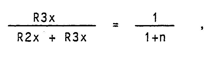
Es sei hier nun einmal angenommen (die Verhältnisse sind in der Tat aber etwas komplizierter, darauf wird noch eingegangen), daß die Hysterese innerhalb dieser Amplitude liegen muß. Dann ist für R2 und R3 zu erhalten:
dU = 1V = |2U₊| = 5V x R3/(R2+R3).So with three short circuits the voltage would be reduced to 1/4, with four short circuits to 1/5 etc., i.e. to 1Vpp.
It should be assumed here (the situation is indeed somewhat more complicated, which will be discussed later) that the hysteresis must lie within this amplitude. Then for R2 and R3 you get:
dU = 1V = | 2U₊ | = 5V x R3 / (R2 + R3).
Man erhält für das Widerstandsverhältnis: R3/(R2+R3) = 1/5. Das ist in erster Näherung der Rechengang für die Bemessung der Hysterese. Als Nächstes soll jetzt auf die etwas komplizierteren Verhältnisse im Verbund aller Treiberstufen eingegangen werden.For the resistance ratio one obtains: R3 / (R2 + R3) = 1/5. In a first approximation, this is the calculation process for dimensioning the hysteresis. The next step is to deal with the somewhat more complicated situation in the combination of all driver stages.
Bisher wurde derart genähert, daß die Widerstände R2 und R3 auch in ihrer gesamten Parallelschaltung entlang der Busleitung wesentlich größer als die Serienwiderstände angenommen wurden.So far it has been approximated that the resistors R2 and R3 have been assumed to be substantially larger than the series resistors in their entire parallel connection along the bus line.
Zunächst ein Kriterium für die Bemessung des Serienwiderstandes R1:
Die Eingangskapazität eines bidirektionalen Bustreibers beträgt etwa im Falle von FACT 15 pF. Das ergibt bei 28 Steckplätzen eine Gesamtkapazität von 420 pF. Will man diese in ca. 4 nS umladen (wesentlich kürzer als eine Taktperiode des Datensignals), dann erhält man grob für den Serienwiderstand = 10 Ohm.
Außerdem muß, wie gesagt, jeder Treiber die Parallelschaltung aus allen Hysteresespannungsteilern treiben. Diese kann man zwar in der Tat so hochimpedant bemessen, daß sie vernachlässigbar sind, also die volle Amplitude an den Eingängen der Empfänger ansteht. Andererseits ist es vorteilhaft, wenn die Parallelschaltung aller Teiler in die Größenordnung des Leitungs-Wellenwiderstandes fällt, weil dann signaltechnische Verbesserungen zu erwarten sind. Jeder sendende Treiber "sieht" dann nämlich in beiden Busrichtungen Werte mit Wellenwiderstandsgrößenordnung, was Reflexionen reduziert. Hinzu addiert sich noch der große Dämpfungsbelag entlang der Leitung, was noch einmal Reflexionen entgegenwirkt. Andererseits tritt dann auch wiederum Spannungsteilung zwischen dem Serienwiderstand des Treibers und den Hystereseteilern auf. Hier ist bei der Bemessung nach Möglichkeit ein Optimum zu finden.
Ein weiterer Vorteil ist, daß, haben die Spannungen an den Empfängern erst einmal während eines Flankenvorganges die Schwelle erreicht, die Empfänger beim Umladen mithelfen, da sie auf Grund der Rückkopplung über den Widerstand R2 auf den Bus zurückwirken. Alle Empfänger wirken somit als Bus-Repeater, ein Vorteil, der in Bezug auf die Sauberkeit des Signals nicht zu unterschätzen ist. Quantifiziert läßt sich die Spannungsteilung durch die Hysteresewiderstände wie folgt ausdrücken:
Ue = Uq x (Rh/28)/(Rh/28 + R1) ;
Darin sind:
Ue die Spannung am Empfänger,
Uq die FACT-Quellenspannung (5Vss),
Rh die Parallelschaltung aus den Spannungsteilerwiderständen R2 und R3.First a criterion for the design of the series resistance R1:
The input capacity of a bidirectional bus driver is approximately 15 pF in the case of FACT. With 28 slots, this gives a total capacitance of 420 pF. If you want to reload it in approx. 4 nS (much shorter than one clock period of the data signal), you get roughly for the series resistance = 10 Ohm.
In addition, as I said, each driver must drive the parallel connection from all hysteresis voltage dividers. In fact, these can be dimensioned so high-impedance that they are negligible, i.e. the full amplitude is present at the inputs of the receivers. On the other hand, it is advantageous if the parallel connection of all the dividers falls within the range of the line impedance, because improvements in signal technology can then be expected. Each sending driver then "sees" values in both bus directions with wave resistance magnitude, which reduces reflections. In addition, there is the large damping layer along the line, which counteracts reflections again. On the other hand, voltage sharing then occurs between the series resistance of the driver and the hysteresis dividers. Here is the design after Possibility to find an optimum.
Another advantage is that once the voltages at the receivers have reached the threshold during an edge process, the receivers help with the reloading, since they act back on the bus due to the feedback via the resistor R2. All receivers thus act as bus repeaters, an advantage that should not be underestimated in terms of signal cleanliness. The voltage division quantified by the hysteresis resistances can be expressed as follows:
Ue = Uq x (Rh / 28) / (Rh / 28 + R1);
In it are:
Ue the voltage at the receiver,
Uq the FACT source voltage (5Vpp),
Rh the parallel connection of the voltage dividing resistors R2 and R3.
Vernachlässigt wurde hierbei die Spannungsteilung zwischen R1 und Rh, welche um Größenordnungen im Wert auseinanderliegen. Bei allem werden jetzt nur die Flanken betrachtet, die Kondensatoren C1, C2, ... also als wechselspannungsmäßiger Kurzschluß angesehen.
Eine erneute Hysterese tritt jetzt durch die Spannungsteilung zwischen R1 und Rh/28 auf. Sie wächst in dem Sinne, wie Rh bzw. Rh/28 abnimmt. Bei den erwähnten vier zulässigen Kurzschlüssen (Uq′ = Uq/5) muß ein Empfänger noch störungsfrei über die Schwelle gesteuert werden. Nimmt man wiederum - worst case - den eingeschwungenen Zustand an, also eine lange Zeit auf dem Bus anstehende "0" oder "1", so ist ein Hub von minimal 0,5 Volt hierzu notwendig, wenn man bei dem oben berechneten Verhältnis R3/(R2+R3) bleibt, weil diese Widerstände dann das Eingangspotential um diesen Wert von der Schwelle nach oben oder unten eingestellt haben. Ist also Uq′ = Uq/5 = 1Vss, so ist die dazugehörige Quellenimpedanz (vier Kurzschlüsse) 1/5 x R1 = 2 Ohm. Damit nun Ue auf die Hälfte absinkt, darf Rh/28 ebenfalls mit 2 Ohm angesetzt werden, also Rh = 56 Ohm. Das ist ohne Frage ein recht theoretischer Wert, da
- 1) die Treiber keine verschwindende Ausgangsimpedanz haben, und
- 2) die Leistungsaufnahme für das Bushandling und die thermische Belastung aus Gründen der Zuverlässigkeit nicht zu hoch angesetzt werden darf.
A new hysteresis now occurs due to the voltage division between R1 and Rh / 28. It grows in the sense that Rh and Rh / 28 decrease. With the four permitted short circuits mentioned (Uq ′ = Uq / 5), a receiver must still be controlled without interference via the threshold. If you assume - in the worst case - the steady state, ie "0" or "1" that has been present on the bus for a long time, a stroke of at least 0.5 volt is necessary if you use the ratio R3 / (R2 + R3) remains because these resistors then increase the input potential by this value from the Have set the threshold up or down. So if Uq ′ = Uq / 5 = 1Vss, then the associated source impedance (four short circuits) is 1/5 x R1 = 2 ohms. So that Ue now drops to half, Rh / 28 may also be set at 2 ohms, i.e. Rh = 56 ohms. There is no question that this is quite a theoretical value, because
- 1) the drivers have no vanishing output impedance, and
- 2) the power consumption for bus handling and the thermal load must not be set too high for reasons of reliability.
Da außerdem die kritische Hysteresegrenze nicht unbedingt erreicht werden soll, sei das Kriterium "Wellenwiderstandsbetrachtung" zur Hand genommen. Danach sollte ein Treiber, speist er in der Mitte des Busses ein Signal ein, nach beiden Seiten hin den Leitungswellenwiderstand "sehen". Sei dieser z.B. 200 Ohm, so ergibt sich mit beiden Hälften 100 Ohm, demnach für Rh/28 = 100 Ohm und für Rh = 2,8 KOhm. Daraus resultiert die Bemessung für die Widerstände in der Zeichnung:
R2 = 12 KOhm,
R3 = 3,3 KOhm.
Damit beträgt die Spannungsteilung zwischen R1 und Rh/28 aber jetzt lediglich maximal:
Ue = Uq/(n+1) x 100/( 100 + 10/(n+1)) = 0,5 V ;
(n sei wiederum die Anzahl der Kurzschlüsse).
Das ergibt ein n von maximal acht Kurzschlüssen. Diese Grenze sollte aber nicht erreicht werden.In addition, since the critical hysteresis limit should not necessarily be reached, the criterion "wave impedance analysis" should be used. After that, a driver should feed a signal in the middle of the bus and "see" the line impedance on both sides. For example, if this is 200 ohms, the result is 100 ohms with both halves, thus for Rh / 28 = 100 ohms and for Rh = 2.8 K ohms. This results in the dimensioning for the resistances in the drawing:
R2 = 12 KOhm,
R3 = 3.3 KOhm.
The voltage division between R1 and Rh / 28 is now only a maximum:
Ue = Uq / (n + 1) x 100 / (100 + 10 / (n + 1)) = 0.5 V;
(n again be the number of short circuits).
This results in an n of a maximum of eight short circuits. However, this limit should not be reached.
Die Stromaufnahme der verwendeten Bustreiber ist nahezu ausschließlich durch die äußere Beschaltung bestimmt. Die vorgestellte Schnittstellenanordnung ist zur Anwendung in MOBS- (modular onboard switching) Systemen in Satelliten ideal geeignet, insbesondere da sich Fehler bei Widerständen fast immer nur durch eine Unterbrechung äußern und selbst Kurzschlüsse bei den Serienkondensatoren sich erst dann nachteilig auswirken, wenn auch noch der beigeordnete Treiber durch Kurzschluß ausfällt. Dieser Fall tritt jedoch mit einer sehr geringen Verbundwahrscheinlichkeit ein.The current consumption of the bus drivers used is almost exclusively determined by the external wiring. The The interface arrangement presented is ideally suited for use in MOBS (modular onboard switching) systems in satellites, especially since faults in resistors are almost always only manifested by an interruption and even short circuits in the series capacitors only have a negative effect if the associated driver is also involved fails due to short circuit. However, this case occurs with a very low probability of association.
Die Gleichspannungsabtrennung kann auch anders als zuvor geschildert erfolgen, z.B. durch einen Übertrager Ü1, Ü2, ... (Fig. 2). Dessen Sekundärwicklung w2 kann beispielsweise direkt an den Bus angeschlossen werden.
Die Primärwicklung w1 (des Übertragers Ü1) ist mit ihrem einen Anschlußende an den Treibereingang E21 und mit ihrem anderen Anschlußende an den Teilerabgriff des aus den Widerständen R21, R31, bzw. R22, R32 ... bestehenden Spannungsteilers angeschlossen. Für die Bemessung der Spannungsteilerwiderstände ist davon auszugehen, daß sie einerseits so hochohmig sein müssen, daß der Kurzschluß eines Treibers nicht als Kurzschluß oder zu niedrige Impedanz auf den Bus transformiert wird, aber andererseits auch so niederohmig sein müssen, daß ein Treiber in Senderichtung genug Leistung auf den Bus transformieren kann, um alle anderen als Empfänger betriebenen Treiber über die ihnen zugeordneten Übertrager anzusteuern. Im Realfall wird nicht die gesamte Treiberleistung wegen Streuverlusten der Übertrager auf den Bus übertragen. Diese Forderungen sind erfüllt, wenn die wechselspannungsmäßige Parallelimpedanz der Widerstände R2 und R3 in der Größenordnung von 100 Ohm liegt. Als Übertrager Ü eignet sich vorzugsweise ein Hochfrequenz-Ferritkern-Übertrager. Die Realisierung mittels eines Übertragers als Gleichspannungsabtrennmittel erfordert weniger Bauelemente als die zuvor vorgestellte Lösung mit Gleichspannungsabtrennkondensator. Die Ausfallwahrscheinlichkeit der Hochfrequenz-Ferritkernübertrager läßt sich durch spezielle Aufbaumaßnahmen (Vergießen, Wickelanordnung mit großem Windungsabstand) erniedrigen.The DC voltage isolation can also be carried out differently than previously described, for example by a transformer U1, U2, ... (FIG. 2). Its secondary winding w2 can be connected directly to the bus, for example.
The primary winding w1 (of the transformer U1) is connected with its one connection end to the driver input E21 and with its other connection end to the divider tap of the voltage divider consisting of the resistors R21, R31, or R22, R32. For the dimensioning of the voltage divider resistors, it must be assumed that on the one hand they must be so high-resistance that the short circuit of a driver is not transformed to the bus as a short circuit or too low impedance, but on the other hand it must also be so low-resistance that a driver has enough power in the direction of transmission can transform to the bus in order to control all other drivers operated as receivers via their assigned transmitters. In real cases, not all of the driver power is transferred to the bus due to leakage losses from the transformers. These requirements are met if the AC parallel impedance of the resistors R2 and R3 is in the order of 100 ohms. A high-frequency ferrite core transformer is preferably suitable as the transformer Ü. The implementation by means of a transformer as a DC voltage isolation means requires fewer components than the solution presented above with a DC voltage isolation capacitor. The The probability of failure of the high-frequency ferrite core transformers can be reduced by special construction measures (casting, winding arrangement with a large winding spacing).
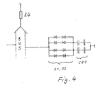
In einer Ausgestaltung der Erfindung ist der Bus beidseitig mit Bauelementen mit Schwellwertverhalten abgeschlossen. Im Ausführungsbeispiel nach Fig. 3 bestehen diese Bauelemente aus antiparallel gegen Massepotential geschalteten Dioden D1, D2 am oberen sowie ebenfalls antiparallel geschalteten Dioden D3, D4 am unteren Busende. Die Schwellenspannung US dieser Bauelemente - hier Dioden - muß größer sein als der Hysteresehub UH der Hysteresebeschaltung für die Treiber T1, T2, ... . Beträgt der Hysteresehub UH beispielsweise 0,625 V, so können Siliziumdioden mit einer Schwellenspannung von US = 0,7 V verwendet werden. Für Signalamplituden auf dem Bus kleiner als 0,7 V ist der Bus "offen"; d.h. es ist nur der ohmsche Bus-Erdungswiderstand R4 wirksam. Steigen die Signalamplituden auf dem Bus über US an, werden die überschüssigen Amplitudenanteile bei ± 0,7 V abgeschnitten. Tritt nun ein Kurzschluß auf, z.B. an einem Bustreiberausgang, so ist der Bus wechselspannungsmäßig zusätzlich mit dem entsprechenden Widerstand R11 ... R128, an dessen Treiber der Kurzschluß auftritt, belastet. Dies reduziert die Signalamplituden auf dem Bus. Der entsprechende Widerstand R11 ... R128 übernimmt dann den Busabschluß. Bei einem solchen Kurzschluß können durch die Belastung mit einem der Widerstände R11 ... R128 die Signalamplituden auf dem Bus, die zuvor ausreichend waren um die Dioden D1, D2, D3 und D4 durchzusteuern, soweit absinken, daß der Schwellwert US nicht mehr erreicht wird. Bei sehr hohen Signalamplituden auf dem Bus wird trotz zusätzlicher Belastung durch einen der Widerstände R11 ... R128 der Schwellwert US erreicht, und es kommt zu einem sogenannten Spannungsteilerverhalten:
Der Bus ist dann sowohl mit dem entsprechenden Widerstand R11 ... R128 als auch mit dem Bahnwiderstand der Dioden D1, D2, D3 bzw. D4 abgeschlossen. Der Widerstand R4 ist um mehrere Größenordnungen größer als die Widerstände R11 ... R128 und die Bahnwiderstände der Dioden D1, D2, D3 bzw. D4, so daß er am Spannungsteilerverhalten nicht mitwirkt. Vorteilhaft ist es, in Serie zu jeweils einem Begrenzerdiodenpaar D1, D2 oder D3, D4 einen Gleichspannungsabtrennkondensator CB1 bzw. CB2 gegen Massepotential zu schalten. Diese Kondensatoren CB1 und CB2 müssen kapazitätsmäßig so groß gewählt werden, daß der Gleichspannungswert für die Hysteresebeschaltungen noch aus den Flanken der übertragbaren Daten regenerierbar ist. Am besten wählt man die Kondensatoren CB1 und CB2 jeweils so groß wie die Kondensatoren C1 bis C28.In one embodiment of the invention, the bus is closed on both sides with components with threshold value behavior. In the exemplary embodiment according to FIG. 3, these components consist of diodes D1, D2 connected antiparallel to ground potential at the upper end and also antiparallel connected diodes D3, D4 at the lower end of the bus. The threshold voltage U S of these components - here diodes - must be greater than the hysteresis stroke U H of the hysteresis circuit for the drivers T1, T2, .... If the hysteresis stroke U H is, for example, 0.625 V, then silicon diodes with a threshold voltage of U S = 0.7 V can be used. The bus is "open" for signal amplitudes on the bus less than 0.7 V; ie only the ohmic bus ground resistance R4 is effective. If the signal amplitudes on the bus rise above U S , the excess amplitude components are cut off at ± 0.7 V. If a short circuit now occurs, for example at a bus driver output, the bus is additionally loaded in terms of AC voltage with the corresponding resistor R11 ... R128, at whose driver the short circuit occurs. This reduces the signal amplitudes on the bus. The corresponding resistor R11 ... R128 then takes over the bus termination. In the event of such a short circuit, the signal amplitudes on the bus, which were previously sufficient to control the diodes D1, D2, D3 and D4, can drop to such an extent that the threshold value U S no longer reaches due to the load with one of the resistors R11 ... becomes. In the case of very high signal amplitudes on the bus, the threshold value U S is reached despite additional loading by one of the resistors R11 ... R128, and what is known as a voltage divider behavior occurs:
The bus is then terminated both with the corresponding resistor R11 ... R128 and with the path resistance of the diodes D1, D2, D3 and D4. The resistor R4 is several orders of magnitude larger than the resistors R11 ... R128 and the path resistances of the diodes D1, D2, D3 and D4, so that it does not participate in the voltage divider behavior. It is advantageous to connect a DC isolating capacitor CB1 or CB2 to ground potential in series with a pair of limiter diodes D1, D2 or D3, D4. These capacitors CB1 and CB2 must be chosen so large in terms of capacity that the DC voltage value for the hysteresis circuits can still be regenerated from the edges of the transferable data. It is best to choose capacitors CB1 and CB2 each as large as capacitors C1 to C28.
Zur Erhöhung der Fehlertoleranz, insbesondere für die Anwendung in Satelliten, ist es zweckmäßig, die Dioden D1 bis D4 und die Kondensatoren CB1 und CB2 mehrfach vorzusehen. Ein solches Ausführungsbeispiel für einen einseitigen Busabschluß zeigt Fig. 4. Hier sind zwei Serienparallelschaltungen von Dioden antiparallel zueinander angeordnet. Der entsprechende Gleichspannungsabtrennkondensator besteht aus vier Teilkondensatoren - je zwei in Serie geschalteten Kondensatoren, die zu einer Parallelschaltung vereinigt sind. Natürlich muß bei diesen Schaltungsvarianten darauf geachtet werden, daß der entsprechende Schwellwert US und die Gesamtkapazität CB1 bzw. CB2 auf den Bus und die übrigen Bauelemente abgestimmt ist.To increase the fault tolerance, in particular for use in satellites, it is advisable to provide the diodes D1 to D4 and the capacitors CB1 and CB2 several times. Such an exemplary embodiment for a one-sided bus termination is shown in FIG. 4. Here two series parallel connections of diodes are arranged antiparallel to each other. The corresponding DC isolating capacitor consists of four partial capacitors - two capacitors connected in series, which are combined to form a parallel connection. Of course, with these circuit variants, care must be taken to ensure that the corresponding threshold value U S and the total capacitance CB1 and CB2 are matched to the bus and the other components.
Durch die Maßnahmen nach der Erfindung ist ein amplitudenabhängiger passiver dynamischer Busabschluß realisierbar, der zur wirksamen Stabilisierung der Signalamplituden auf dem Bus führt.The measures according to the invention make it possible to implement an amplitude-dependent passive dynamic bus termination which leads to the effective stabilization of the signal amplitudes on the bus.
Anstelle des Busabschlusses mit Bauelementen mit Schwellwertverhalten können die Spannungsteilerwiderstände R31, R32, ... zwischen jeweils dem busnahen Treibereingang E21, E22, ... und Stromversorgung bezüglich jener Treiber, die in der Nachbarschaft eines Busendes angeordnet sind - z.B. die letzten 2 oder 3 Treiber in der Nachbarschaft eines Busendes - so bemessen werden, daß ihr gemeinsamer Parallelwiderstand; d.h. der durch die Parallelschaltung sich bildende Widerstandswert, in etwa dem Wellenwiderstand des Busses entspricht.Instead of terminating the bus with components with threshold value behavior, the voltage divider resistors R31, R32, ... between the driver input E21, E22, ... close to the bus and the power supply with respect to those drivers which are arranged in the vicinity of a bus end - e.g. the last 2 or 3 drivers in the vicinity of a bus end - be dimensioned so that their common parallel resistance; i.e. the resistance value formed by the parallel connection roughly corresponds to the characteristic impedance of the bus.
Claims (10)
R2 den an den busfernen Treibereingang angeschlossenen Spannungsteilerwiderstand,
R3 den an die Stromversorgung angeschlossenen Spannungsteilerwiderstand,
x die Laufvariable 1, 2, 3. ... des jeweiligen Teilnehmers und
n die Zahl der tolerierbaren Kurzschlüsse der Treiber darstellt.1. Bus coupling circuit between a data transmission device (bus) and at least one data transmitter and a data receiver as a subscriber, each subscriber having a bidirectional driver (T1, T2, ...), with DC voltage disconnect means (Cl, C2; R11, R12 ...) between driver (T1, T2, ...) and bus, which simultaneously represent a working impedance for the driver, and each driver (T1, T2, ...) has a hysteresis, characterized in that for each driver ( T1, T2, ...) an additional hysteresis circuit is provided, which consists of a voltage divider (R21, R31; R22, R32 ...) which is active for alternating signals and whose divider chain is connected between the remote input (E11, E12, ...) of the driver (T1, T2, ...) and power supply and its divider tap is connected to the driver input (E21, E22, ...) close to the bus in order to connect directly to the driver (T1, T2, ..), which is free of direct current (e.g. capacitive). .) a DC voltage to the bus and that the voltage divider is dimensioned as follows to achieve a fault-tolerant bus:
R2 the voltage divider resistor connected to the driver input remote from the bus,
R3 the voltage divider resistor connected to the power supply,
x the run variable 1, 2, 3. ... of the respective participant and
n represents the number of tolerable short circuits in the driver.
Applications Claiming Priority (4)
| Application Number | Priority Date | Filing Date | Title |
|---|---|---|---|
| DE19883835458 DE3835458A1 (en) | 1988-10-18 | 1988-10-18 | Interface arrangement for a bus system |
| DE3835458 | 1988-10-18 | ||
| DE3905109 | 1989-02-20 | ||
| DE3905109 | 1989-02-20 |
Publications (3)
| Publication Number | Publication Date |
|---|---|
| EP0364700A2 true EP0364700A2 (en) | 1990-04-25 |
| EP0364700A3 EP0364700A3 (en) | 1992-07-22 |
| EP0364700B1 EP0364700B1 (en) | 1995-05-03 |
Family
ID=25873355
Family Applications (1)
| Application Number | Title | Priority Date | Filing Date |
|---|---|---|---|
| EP89115672A Expired - Lifetime EP0364700B1 (en) | 1988-10-18 | 1989-08-25 | Bus-coupling circuit |
Country Status (4)
| Country | Link |
|---|---|
| US (1) | US4985903A (en) |
| EP (1) | EP0364700B1 (en) |
| CA (2) | CA1337826C (en) |
| DE (1) | DE58909214D1 (en) |
Cited By (4)
| Publication number | Priority date | Publication date | Assignee | Title |
|---|---|---|---|---|
| EP0427921A3 (en) * | 1989-11-14 | 1994-07-27 | Ant Nachrichtentech | Method and device for data transmission |
| WO2000076159A1 (en) * | 1999-06-07 | 2000-12-14 | Siemens Audiologische Technik Gmbh | Interface for providing electrical isolation and for transmitting digital signals |
| WO2001047111A3 (en) * | 1999-12-21 | 2002-02-14 | Teradyne Inc | Capacitively coupled re-referencing circuit with positive feedback |
| US11750176B2 (en) | 2018-11-22 | 2023-09-05 | Robert Bosch Gmbh | Reflection attenuation device for a bus of a bus system, and method for attenuating reflections during a data transfer in a bus system |
Families Citing this family (8)
| Publication number | Priority date | Publication date | Assignee | Title |
|---|---|---|---|---|
| US5134311A (en) * | 1990-06-07 | 1992-07-28 | International Business Machines Corporation | Self-adjusting impedance matching driver |
| WO1993025027A1 (en) * | 1992-06-02 | 1993-12-09 | Siemens Aktiengesellschaft | Subscriber station realized according to the building block technology |
| KR950012306B1 (en) * | 1993-03-25 | 1995-10-16 | 삼성전자주식회사 | Bus arrangement for digital signal processing chip |
| JP2882266B2 (en) * | 1993-12-28 | 1999-04-12 | 株式会社日立製作所 | Signal transmission device and circuit block |
| US5561694A (en) * | 1995-07-26 | 1996-10-01 | International Business Machines Corporation | Self-timed driver circuit |
| IT1278522B1 (en) | 1995-11-27 | 1997-11-24 | Italtel Spa | METHOD AND DEVICE FOR CORRECTING TRANSMISSION ERRORS AND IDENTIFYING THE FAULTY UNITS IN THE CONTEXT OF A DATA TRANSMISSION |
| US6219812B1 (en) * | 1998-06-11 | 2001-04-17 | Sun Microsystems, Inc. | Apparatus and method for interfacing boundary-scan circuitry with DTL output drivers |
| CN105843195B (en) * | 2016-05-24 | 2019-02-01 | 中国科学院长春光学精密机械与物理研究所 | The upper electric control system of multi-controller |
Citations (3)
| Publication number | Priority date | Publication date | Assignee | Title |
|---|---|---|---|---|
| EP0143699A2 (en) * | 1983-11-22 | 1985-06-05 | Digital Equipment Corporation | Bus transceiver |
| DE3433150A1 (en) * | 1984-09-10 | 1986-03-20 | Siemens AG, 1000 Berlin und 8000 München | Interface arrangement for coupling a subscriber circuit to a data transmission line |
| EP0184816A2 (en) * | 1984-12-13 | 1986-06-18 | Honeywell Inc. | Data transmission system |
Family Cites Families (5)
| Publication number | Priority date | Publication date | Assignee | Title |
|---|---|---|---|---|
| GB1200486A (en) * | 1967-04-18 | 1970-07-29 | Int Computers Ltd | Data transmitting apparatus |
| US3875332A (en) * | 1973-12-27 | 1975-04-01 | Nasa | Digital transmitter for data bus communications system |
| DK143627C (en) * | 1978-10-30 | 1982-02-15 | Rovsing A S | WIRELESS CLIP CIRCUIT FOR TRANSMISSION |
| FR2443770A1 (en) * | 1978-12-04 | 1980-07-04 | Materiel Telephonique | Receiver for AC data bus - comprises comparator capacitively coupled to bus lines via DC restoration circuit |
| FR2452207A1 (en) * | 1979-03-20 | 1980-10-17 | Matra | Device coupling transmitter to transmission line - includes transformer secondary whose impedance is reduced from high to low value by short circuiting primary when transmitter is active |
-
1989
- 1989-08-25 DE DE58909214T patent/DE58909214D1/en not_active Expired - Fee Related
- 1989-08-25 EP EP89115672A patent/EP0364700B1/en not_active Expired - Lifetime
- 1989-09-29 CA CA000615005A patent/CA1337826C/en not_active Expired - Fee Related
- 1989-10-17 US US07/422,516 patent/US4985903A/en not_active Expired - Fee Related
- 1989-10-18 CA CA002000919A patent/CA2000919A1/en not_active Abandoned
Patent Citations (3)
| Publication number | Priority date | Publication date | Assignee | Title |
|---|---|---|---|---|
| EP0143699A2 (en) * | 1983-11-22 | 1985-06-05 | Digital Equipment Corporation | Bus transceiver |
| DE3433150A1 (en) * | 1984-09-10 | 1986-03-20 | Siemens AG, 1000 Berlin und 8000 München | Interface arrangement for coupling a subscriber circuit to a data transmission line |
| EP0184816A2 (en) * | 1984-12-13 | 1986-06-18 | Honeywell Inc. | Data transmission system |
Non-Patent Citations (2)
| Title |
|---|
| REGELUNGSTECHNISCHE PRAXIS Bd. 25, Nr. 10, 1983, MUNCHEN,DE B. WIEMANN ET AL.: 'Bussysteme' pages S61 - S64; * |
| REGELUNGSTECHNISCHE PRAXIS Bd. 25, Nr. 11, 1983, MUNCHEN, DE B. WIEMANN ET AL.: 'Bussysteme' pages S69 - S71; * |
Cited By (4)
| Publication number | Priority date | Publication date | Assignee | Title |
|---|---|---|---|---|
| EP0427921A3 (en) * | 1989-11-14 | 1994-07-27 | Ant Nachrichtentech | Method and device for data transmission |
| WO2000076159A1 (en) * | 1999-06-07 | 2000-12-14 | Siemens Audiologische Technik Gmbh | Interface for providing electrical isolation and for transmitting digital signals |
| WO2001047111A3 (en) * | 1999-12-21 | 2002-02-14 | Teradyne Inc | Capacitively coupled re-referencing circuit with positive feedback |
| US11750176B2 (en) | 2018-11-22 | 2023-09-05 | Robert Bosch Gmbh | Reflection attenuation device for a bus of a bus system, and method for attenuating reflections during a data transfer in a bus system |
Also Published As
| Publication number | Publication date |
|---|---|
| DE58909214D1 (en) | 1995-06-08 |
| US4985903A (en) | 1991-01-15 |
| CA1337826C (en) | 1995-12-26 |
| EP0364700B1 (en) | 1995-05-03 |
| CA2000919A1 (en) | 1990-04-18 |
| EP0364700A3 (en) | 1992-07-22 |
Similar Documents
| Publication | Publication Date | Title |
|---|---|---|
| EP0090255B1 (en) | Tristate driver circuit | |
| EP0364700B1 (en) | Bus-coupling circuit | |
| EP0614298A2 (en) | Bussystem protected against the uncoupling of earth connections | |
| DE102015118514A1 (en) | Signal isolator system with protection for common mode transients | |
| WO2006072292A1 (en) | Circuit arrangement and method for protecting a circuit from electrostatic discharges | |
| DE102013222786A1 (en) | Subscriber station for a bus system and method for reducing conducted emissions in a bus system | |
| EP0500557A1 (en) | Multiplex circuit arrangement, in particular for controlling consumer stations in motor vehicles. | |
| DE3311881C2 (en) | ||
| EP1568149A1 (en) | Protective circuit for protection against overvoltage for a can-bus transceiver | |
| EP2110950B1 (en) | Switch and method for transferring signal voltage within a driver of a voltage semiconductor | |
| EP0427921B1 (en) | Method and device for data transmission | |
| DE102010042156A1 (en) | Transmission device for a differential communication | |
| DE2250859C2 (en) | Circuit arrangement for the transition from two-wire to four-wire operation for telecommunications, in particular telephone switching systems | |
| DE69833790T2 (en) | ASYMMETRIC CURRENT DRIVER FOR DIFFERENTIAL TRANSMISSION LINES | |
| DE3835458C2 (en) | ||
| EP0643515B1 (en) | Arrangement for bidirectional transmission of data | |
| DE10305361B4 (en) | Electronic high-frequency switch | |
| WO1990008437A2 (en) | Coupling of a bus subscriber | |
| DE102011053904A1 (en) | Circuit arrangement for protecting controller area network transceivers from communication interfaces for wire-bound communication for protecting power system in e.g. building, has capacitor electrically switched in series to diodes | |
| EP0689291B1 (en) | MOS driver circuit | |
| DE10314514A1 (en) | Power device control circuit | |
| EP3672009B1 (en) | Protection circuit, electronic device and method for operating an electronic device | |
| DE102016011257A1 (en) | Bus and communication system for DC-free signal transmission on a common medium with termination | |
| DE19925909A1 (en) | Interface for electrical isolation and for the transmission of digital signals | |
| EP0082410B1 (en) | Circuit for the suppression of signals on line sections |
Legal Events
| Date | Code | Title | Description |
|---|---|---|---|
| PUAI | Public reference made under article 153(3) epc to a published international application that has entered the european phase |
Free format text: ORIGINAL CODE: 0009012 |
|
| AK | Designated contracting states |
Kind code of ref document: A2 Designated state(s): DE FR GB IT NL |
|
| 17P | Request for examination filed |
Effective date: 19901227 |
|
| PUAL | Search report despatched |
Free format text: ORIGINAL CODE: 0009013 |
|
| AK | Designated contracting states |
Kind code of ref document: A3 Designated state(s): DE FR GB IT NL |
|
| 17Q | First examination report despatched |
Effective date: 19940808 |
|
| GRAA | (expected) grant |
Free format text: ORIGINAL CODE: 0009210 |
|
| ITF | It: translation for a ep patent filed |
Owner name: BARZANO' E ZANARDO MILANO S.P.A. |
|
| AK | Designated contracting states |
Kind code of ref document: B1 Designated state(s): DE FR GB IT NL |
|
| GBT | Gb: translation of ep patent filed (gb section 77(6)(a)/1977) |
Effective date: 19950504 |
|
| REF | Corresponds to: |
Ref document number: 58909214 Country of ref document: DE Date of ref document: 19950608 |
|
| ET | Fr: translation filed | ||
| PLBE | No opposition filed within time limit |
Free format text: ORIGINAL CODE: 0009261 |
|
| STAA | Information on the status of an ep patent application or granted ep patent |
Free format text: STATUS: NO OPPOSITION FILED WITHIN TIME LIMIT |
|
| 26N | No opposition filed | ||
| PGFP | Annual fee paid to national office [announced via postgrant information from national office to epo] |
Ref country code: GB Payment date: 19960809 Year of fee payment: 8 |
|
| PGFP | Annual fee paid to national office [announced via postgrant information from national office to epo] |
Ref country code: FR Payment date: 19960814 Year of fee payment: 8 |
|
| PGFP | Annual fee paid to national office [announced via postgrant information from national office to epo] |
Ref country code: NL Payment date: 19960822 Year of fee payment: 8 |
|
| PGFP | Annual fee paid to national office [announced via postgrant information from national office to epo] |
Ref country code: DE Payment date: 19961024 Year of fee payment: 8 |
|
| PG25 | Lapsed in a contracting state [announced via postgrant information from national office to epo] |
Ref country code: GB Free format text: LAPSE BECAUSE OF NON-PAYMENT OF DUE FEES Effective date: 19970825 |
|
| PG25 | Lapsed in a contracting state [announced via postgrant information from national office to epo] |
Ref country code: NL Free format text: LAPSE BECAUSE OF NON-PAYMENT OF DUE FEES Effective date: 19980301 |
|
| GBPC | Gb: european patent ceased through non-payment of renewal fee |
Effective date: 19970825 |
|
| PG25 | Lapsed in a contracting state [announced via postgrant information from national office to epo] |
Ref country code: FR Free format text: LAPSE BECAUSE OF NON-PAYMENT OF DUE FEES Effective date: 19980430 |
|
| PG25 | Lapsed in a contracting state [announced via postgrant information from national office to epo] |
Ref country code: DE Free format text: LAPSE BECAUSE OF NON-PAYMENT OF DUE FEES Effective date: 19980501 |
|
| NLV4 | Nl: lapsed or anulled due to non-payment of the annual fee |
Effective date: 19980301 |
|
| REG | Reference to a national code |
Ref country code: FR Ref legal event code: ST |
|
| PG25 | Lapsed in a contracting state [announced via postgrant information from national office to epo] |
Ref country code: IT Free format text: LAPSE BECAUSE OF NON-PAYMENT OF DUE FEES;WARNING: LAPSES OF ITALIAN PATENTS WITH EFFECTIVE DATE BEFORE 2007 MAY HAVE OCCURRED AT ANY TIME BEFORE 2007. THE CORRECT EFFECTIVE DATE MAY BE DIFFERENT FROM THE ONE RECORDED. Effective date: 20050825 |