EP0364542B1 - An electronic controller for a water purifying unit - Google Patents
An electronic controller for a water purifying unit Download PDFInfo
- Publication number
- EP0364542B1 EP0364542B1 EP89903884A EP89903884A EP0364542B1 EP 0364542 B1 EP0364542 B1 EP 0364542B1 EP 89903884 A EP89903884 A EP 89903884A EP 89903884 A EP89903884 A EP 89903884A EP 0364542 B1 EP0364542 B1 EP 0364542B1
- Authority
- EP
- European Patent Office
- Prior art keywords
- current
- electronic controller
- output
- conductivity
- voltage
- Prior art date
- Legal status (The legal status is an assumption and is not a legal conclusion. Google has not performed a legal analysis and makes no representation as to the accuracy of the status listed.)
- Expired - Lifetime
Links
- XLYOFNOQVPJJNP-UHFFFAOYSA-N water Substances O XLYOFNOQVPJJNP-UHFFFAOYSA-N 0.000 title claims description 50
- 239000000523 sample Substances 0.000 claims description 60
- 239000008399 tap water Substances 0.000 claims description 19
- 235000020679 tap water Nutrition 0.000 claims description 19
- 238000000746 purification Methods 0.000 claims description 14
- 239000008213 purified water Substances 0.000 claims description 13
- 239000003990 capacitor Substances 0.000 claims description 9
- 238000012544 monitoring process Methods 0.000 claims description 7
- 230000004044 response Effects 0.000 claims description 6
- 230000008878 coupling Effects 0.000 claims description 2
- 238000010168 coupling process Methods 0.000 claims description 2
- 238000005859 coupling reaction Methods 0.000 claims description 2
- 238000012360 testing method Methods 0.000 abstract description 62
- 230000006870 function Effects 0.000 description 9
- 239000012528 membrane Substances 0.000 description 6
- 238000005304 joining Methods 0.000 description 5
- 230000008859 change Effects 0.000 description 4
- 238000001914 filtration Methods 0.000 description 4
- 230000009471 action Effects 0.000 description 3
- 238000013461 design Methods 0.000 description 3
- 238000005868 electrolysis reaction Methods 0.000 description 3
- 238000002955 isolation Methods 0.000 description 3
- 238000003860 storage Methods 0.000 description 3
- 230000007704 transition Effects 0.000 description 3
- 238000010586 diagram Methods 0.000 description 2
- 239000012535 impurity Substances 0.000 description 2
- 238000007689 inspection Methods 0.000 description 2
- 238000001223 reverse osmosis Methods 0.000 description 2
- ZAMOUSCENKQFHK-UHFFFAOYSA-N Chlorine atom Chemical compound [Cl] ZAMOUSCENKQFHK-UHFFFAOYSA-N 0.000 description 1
- WHXSMMKQMYFTQS-UHFFFAOYSA-N Lithium Chemical compound [Li] WHXSMMKQMYFTQS-UHFFFAOYSA-N 0.000 description 1
- 206010049155 Visual brightness Diseases 0.000 description 1
- 230000032683 aging Effects 0.000 description 1
- 230000002457 bidirectional effect Effects 0.000 description 1
- 230000015572 biosynthetic process Effects 0.000 description 1
- 229910052801 chlorine Inorganic materials 0.000 description 1
- 239000000460 chlorine Substances 0.000 description 1
- 230000000295 complement effect Effects 0.000 description 1
- 238000010411 cooking Methods 0.000 description 1
- 230000003111 delayed effect Effects 0.000 description 1
- 238000007599 discharging Methods 0.000 description 1
- 230000035622 drinking Effects 0.000 description 1
- 230000001747 exhibiting effect Effects 0.000 description 1
- 229930195733 hydrocarbon Natural products 0.000 description 1
- 150000002430 hydrocarbons Chemical class 0.000 description 1
- 229910052744 lithium Inorganic materials 0.000 description 1
- 238000004519 manufacturing process Methods 0.000 description 1
- 239000000463 material Substances 0.000 description 1
- 238000000034 method Methods 0.000 description 1
- 239000013618 particulate matter Substances 0.000 description 1
- 239000002244 precipitate Substances 0.000 description 1
- 238000011045 prefiltration Methods 0.000 description 1
- 230000008569 process Effects 0.000 description 1
- 239000012264 purified product Substances 0.000 description 1
- 230000009467 reduction Effects 0.000 description 1
- 230000001105 regulatory effect Effects 0.000 description 1
- 238000005070 sampling Methods 0.000 description 1
- -1 scale Substances 0.000 description 1
- 238000012216 screening Methods 0.000 description 1
- 239000000126 substance Substances 0.000 description 1
- 230000001052 transient effect Effects 0.000 description 1
- 239000002351 wastewater Substances 0.000 description 1
Images


Classifications
-
- B—PERFORMING OPERATIONS; TRANSPORTING
- B01—PHYSICAL OR CHEMICAL PROCESSES OR APPARATUS IN GENERAL
- B01D—SEPARATION
- B01D65/00—Accessories or auxiliary operations, in general, for separation processes or apparatus using semi-permeable membranes
- B01D65/10—Testing of membranes or membrane apparatus; Detecting or repairing leaks
- B01D65/104—Detection of leaks in membrane apparatus or modules
-
- B—PERFORMING OPERATIONS; TRANSPORTING
- B01—PHYSICAL OR CHEMICAL PROCESSES OR APPARATUS IN GENERAL
- B01D—SEPARATION
- B01D61/00—Processes of separation using semi-permeable membranes, e.g. dialysis, osmosis or ultrafiltration; Apparatus, accessories or auxiliary operations specially adapted therefor
- B01D61/02—Reverse osmosis; Hyperfiltration ; Nanofiltration
- B01D61/12—Controlling or regulating
-
- C—CHEMISTRY; METALLURGY
- C02—TREATMENT OF WATER, WASTE WATER, SEWAGE, OR SLUDGE
- C02F—TREATMENT OF WATER, WASTE WATER, SEWAGE, OR SLUDGE
- C02F1/00—Treatment of water, waste water, or sewage
- C02F1/44—Treatment of water, waste water, or sewage by dialysis, osmosis or reverse osmosis
-
- C—CHEMISTRY; METALLURGY
- C02—TREATMENT OF WATER, WASTE WATER, SEWAGE, OR SLUDGE
- C02F—TREATMENT OF WATER, WASTE WATER, SEWAGE, OR SLUDGE
- C02F2209/00—Controlling or monitoring parameters in water treatment
- C02F2209/05—Conductivity or salinity
Definitions
- This invention relates generally to a water purifying unit incorporating a filter, and more particularly to an electronic controller for a water purifying unit for providing monitoring and test functions for indicating, for example, when the filter should be replaced.
- Some typical prior art water purification systems include, in addition to a filter in the form of a reverse osmosis membrane, a pre-filter for initial screening of the feed or tap water to protect the membrane from clogging, and a post-filter for further purification, especially for the removal of organics such as dissolved hydrocarbons.
- the tap or feed water is filtered and separated into purified water and waste water. Since the filters constitute a major restriction in the water purification system, the filtration process is relatively slow. Therefore, a system of a size which is economically and esthetically practical for the home and the work place is generally not able to generate adequate amounts of water on demand, but must include a water storage reservoir.
- the prior art relative to water purification systems, includes U. S. Patent No. 3,838,774, which issued to Dolan et al.
- This patent discloses an apparatus for monitoring water purification systems.
- the system typically includes an inlet chamber for receiving tap water, an outlet chamber for receiving purified water, and a membrane separating the inlet and outlet chambers for filtering the tap water as it passes from the inlet chamber to the outlet chamber.
- a conductivity sensing probe operatively associated with the inlet side, senses the electrical conductivity of the tap water.
- a similar sensing probe associated with the outlet side, senses the electrical conductivity of the purified water.
- the conductivity sensing probes are powered by an electrical source and develop output signals that are compared against a known threshold. The output comparison is also viewable on a meter, recorder, and/or alarm device to continuously indicate the effectiveness of the filtering system.
- the conductivity sensing probe on the inlet side is connected in the negative feedback path of an operational type amplifier and the conductivity sensing probe on the outlet side is connected across the negative and positive inputs of the amplifier.
- the output voltage of the amplifier is proportional to the ratio of the conductivity of the purified water to the conductivity of the tap water; which ratio, in turn, is a continuous measure of the relative impurity levels.
- US-A-4,587,518 describes a monitor and control system for water purification apparatus which includes first and second conductivity cells located in the input water path and the purified product water path of the apparatus, respectively.
- the conductivity cells produce output signals exhibiting amplitudes representative of the impurity concentrations in the respective water paths.
- a disadvantage of the continuously monitoring type systems is that power consumption for operating such systems is extremely high.
- a serious disadvantage of the continuously-monitoring type systems disclosed in the prior art is that the power consumption for operating such systems is extremely high. Where batteries are used as the power supply, the high continuous current drain of such systems would soon drain the battery, requiring battery replacement, or a costly battery charging system to keep the battery fully charged.
- a further disadvantage of the prior art systems is the lack of a straightforward means to compensate for the inevitable differences in probe calibration factors which may vary because of design, material and/or manufacturing differences.
- the electronic controller of the present invention as defined in claim 1 is particularly adapted for use with a water purifying unit of the type having a tap water inlet, a purified water outlet, a reservoir, a filter interposed between the water inlet and outlet through which the tap water passes for purification, a first conductivity probe in the tap water for sensing the salinity of the tap water, and a second conductivity probe in the purified water for sensing the salinity of the purified water.
- the first and second conductivity probes having a common input.
- the electronic controller is comprised of: a current source coupled to the first and second conductivity probes for intermittently applying a current pulse thereto resulting in current signals from the probes in the ratio of the relative conductivities (salinity) of the water samples in which they are immersed; and electrical converting means for developing voltages indicative of probe currents; and voltage amplifying means to cause the voltage due to current in the second probe to be just equal to the voltage due to current in the first probe when the filter has just deteriorated to the point where it should be replaced; and electrical comparing means for comparing the voltage output signals from the first and second conductivity probe circuits and for generating a positive output voltage when the voltage output signal from the first conductivity probe exceeds the voltage output signal from the second conductivity probe circuit indicating that the filter is all right, and for generating a negative output voltage when the voltage output signal from the first conductivity probe circuit is below the voltage output signal from the second conductivity probe circuit for indicating that the filter should be replaced;and electrical switching means responsive to an input
- the electronic controller 100 of the present invention is comprised of an analog chip 200 and a digital chip 300.
- the chips are application specific integrated circuits, commonly referred to as ASIC chips.
- the analog chip 200 was fabricated by the Raytheon Co. from their basic RLA 80 series die as number (RA8034) ASIC chip and the digital chip 300 was fabricated by Texas Instruments as their CF61578 ASIC chip.
- the electronic controller 100 is powered by a single 9 v. lithium battery 10 which because of the low current drain of the controller will provide more than one year of service before replacement is needed.
- the analog ASIC chip 200 has four principal sections: power control 20, conductivity test 30, LED drivers 40, and bias networks 50.
- the power control section 20 has two major functions; first, it is a very low drain voltage regulator for providing a constant + 5 V. to the digital ASIC chip 300, and second it performs a switching function for turning on supply power in response to a conductivity test signal.
- the first function is necessary in order to keep the current drain of the digital ASIC chip 300 to a consistently low value even when the battery is fresh.
- the digital ASIC chip 300 would have a higher current drain at voltages above 5 volts and may even be damaged by the full voltage of a fresh 9 volt battery.
- the second function is performed by an electronic switch that is activated by a conductivity test signal from the digital ASIC 300 to turn on the supply power to the conductivity test 30 and bias networks 50 sections of this chip when a conductivity test is to be performed and to turn off the supply power at the end of the test.
- This function is necessary because the conductivity test section 30 has a large current drain (2-4 ma) and is therefore activated for only 4 seconds of each 8-minute cycle during a reservoir fill cycle. (details of this operation will be described later in the specification)
- the power control section 20 which is on-line all the time, have a very low current drain.
- the power control section 20 additionally generates an artificial electrical ground potential Vg which is midway between the negative battery terminal potential -Vs and the switched positive battery supply voltage +Vs for a purpose to be designated hereinafter.
- the conductivity test section 30 measures the ratio of the conductivity of the purified water to the conductivity of the tap water. When this ratio rises above a selected predetermined value, the membrane or filter part of the unit is deemed to be spent and a "failed" test result is communicated to the digital ASIC chip 300. The digital ASIC chip 300 will then change the "service required" status line to cause a "service required” LED 18 to flash.
- the conductivity test circuit 30 is connected to a pair of conductivity probes 62 and 64 by means of a d.c. isolation capacitor C102, at one common end, and by transimpedance amplifiers U4, and U5, respectively, at the other end.
- the isolation capacitor C102 is used to prevent a d.c. current from flowing through the probes which would cause an electrolysis which would affect probe calibration.
- a 2KHz. oscillator and divide by 2 circuit 32 is used to generate a 50% duty cycle square signal at 1KHz.
- a buffer U3 receives the 1KHz square wave signal and provides at its output a signal which is strong enough for actual pull-up and pull-down operation of a current pulser circuit 36 and a comparator and strobe circuit 46.
- the current pulser 36 excites the probes from one common end with a 50% duty cycle, bi-directional square wave of current, so that the current will divide between the two probes exactly in proportion to their conductivities. This division is assisted by the fact that the transimpedance amplifiers U4 and U5 receive the conducted current at virtual ground summing junctions.
- the output signal from amplifier U4 is further amplified by amplifier U6, as it is the smaller of the two conducted currents, to be nominally equal to the larger signal when at the threshold value.
- Amplifier U6 at its negative input is connected to the wiper of the threshold gain adjust pot P101 whose gain setting determines the threshold value for the PASS/FAIL conductivity test.
- the comparator and strobe circuit 46 compares the outputs from the transimpedance amplifier U4 and the output of transimpedance amplifier U5 which has been amplified by amplifier U6 to provide an output indicative of the difference between the two inputs, if any.
- the output signal from the comparator and strobe circuit 46 after filtering by the low-pass filter and discharge current sink 48, is used to activate switch 54, via a comparator U8.
- the switch 54 provides the test result signal to the digital ASIC chip 300 by clamping to the potential - Vs if the test is passed OK and to a high impedance if the test is failed.
- the LED Drivers section 40 provides for the constant current control of the LED indicators 14, 16 and 18 when they are flashed through enablement of (constant current) drivers 22, 24 and 26, respectively, and the occurrence of a strobe signal from LED strobe circuit 28.
- the LED's are enabled to turn on for 15ms of every 2 seconds during the time that a pressure switch (PS1) is closed and that a status line such as fill or service request is activated and the LED strobe signal is received. It is the LED "strobe" signal that is received from the digital ASIC via the strobe circuit 28 which pulls down to -Vs to actually complete the turn on of the LED's.
- each LED (constant current) driver is set to provide a particular level of current drive according to the color of the attached LED; 0.8ma for red, 1.3ma for green, and 2.8ma for yellow.
- the bias networks section 50 is activated when the conductivity test comes ON to provide bias current to all of the amplifiers, U1 through U8, in the analog ASIC chip 200 (shown in Fig. 2).
- the prior description has been related to the system in general and specifically to the function of the major sections of the analog ASIC chip 200.
- the following description will be directed to a detailed circuit level description of the analog ASIC chip 200 made with references to the circuitry shown in Fig. 2 which references will be grouped under the major circuit sections used in the description of Fig.1.
- This section includes the low drain voltage regulator 52 for the supply voltage for the digital ASIC 300 and the electronic power switch 38 for the conductivity test circuit 30.
- bias current sources consisting of transistors Q30-Q36, which form the bias circuit 34 and the ground regulator which is based on an operational amplifier U1.
- the bias circuit 34 is designed to minimize the variation of output currents as the battery ages.
- This circuit is a multiple-output current mirror, with one of the outputs, Q33 and Q34 being a 2x current output by virtue of paralleling two transistors of the same die size as used for transistors Q35 and Q36.
- the current sources work from an input reference voltage consisting of two Vbe drops below +Vbat that occurs in transistors Q30 and Q31.
- the Vbe drop of transistor Q32 will offset the Vbe drop in Q30 thus leaving a net reference of one Vbe drop from Q31.
- the input current to the multiple output mirror then is determined by one Vbe drop divided by the resistance of R25 which is approximately 2.3 ua.
- Transistors Q33 and Q34 being in parallel will source about 2 x 2.3 ua which equates to 4.6 ua, but Q35 and Q36 will each mirror the 2.3 ua input current. Due to variations in +Vbat the current to Q30 and Q31 will vary considerably as the battery ages, but the source currents from Q32-Q36 will vary only slightly with battery life since the mirror input current is determined by R25 and one Vbe drop which will change only slightly with the input current to Q30 and Q31.
- the 4.6ua output current is used to bias the voltage regulator reference circuit and the 2.3ua output current of Q35 is used as a pull up on the TEST CONDUCTIVITY input from the digital ASIC 300.
- the TEST CONDUCTIVITY input can never pull up to more than Q41′s Vbe so the digital ASIC 300 TEST CONDUCTIVITY output will never be exposed to the full +Vbat.
- the external 1.2M resistor R101 is used because there are no high value resistors available on the ASIC dies.
- the voltage regulator 52 is a simple emitter follower regulator using Q42 as a series pass transistor.
- the reference voltage at the base of Q42 is developed with a Vbe multiplier consisting of Q43, R28, and R102.
- Vbe multiplier consisting of Q43, R28, and R102.
- the power switch for the conductivity test uses three NPNS transistors in parallel Q37-39 which are driven by a PNPS transistor Q40.
- Current source Q36 to the base of Q40 and resistor R27 from the base to emitter of Q37-39 assures complete turnoff when the switch is open.
- the switch will close whenever the signal on the TEST CONDUCTIVITY line is high (impedance) and the 2.3ua bias current from Q35 has turned on Q41 which in turn turns on Q40 and Q37-Q39.
- the output +Vs at the emitters of Q37-Q39 will be a few tenths of a volt below +Vbat.
- the ground regulator 42 is configured to force the mid-point voltage between +Vs and -Vs to be at ground potential.
- the mid-point is determined by the voltage divider of R32 and R33 whose common node feeds the + input of the operational amplifier U1.
- the battery terminal voltages are otherwise free to float with respect to ground except for the action of the ground regulator which is active only during the conductivity test.
- the -Vs terminal is the common supply point between the analog ASIC chip 200 and the digital ASIC chip 300 and therefore the digital ASIC power is essentially floating with respect to ground most of the time.
- This section is to periodically test the conductivity of the incoming (dirty) and processed (purified) water, and to enable the LED 18 when the processed water conductivity exceeds 25% or other selected threshold percentage of the incoming water conductivity. Besides low battery drain, two other considerations influenced this design.
- the conductivity of the incoming water as indicated by the resistance of probe 64 ranges from 476 ohms to 25K ohms, a ratio of over 50:1. If the signals to be compared for ratio were to each have a 50:1 range, then it would be difficult to maintain good gain accuracy for the small signals in the presence of voltage offsets and offset bias currents in the operational amplifier stages. Therefore, the probes 62 and 64 are excited with a current source so that when the measured currents are converted to voltages by transimpedance amplifiers U4-U5, the sum of the two signals would be a constant rather than ranging over a 50:1 ratio.
- d.c. current should not be allowed to flow in probes 62 and 64 because the resulting electrolysis could affect probe calibration. Accordingly, the probes are excited with a 50% duty-cycle bidirectional square wave of current which is capacitively coupled (to eliminate d.c.) to the probes.
- the current will divide between the two probes exactly in proportion to their conductivities. These currents are then converted to voltages which are compared for ratio by amplifying the smaller signal to be nominally equal to the larger signal when at threshold and then by comparing signal magnitudes.
- the test chain begins with a 2KHz oscillator which includes U2,C101, and R1-R3.
- a small positive feedback voltage is provided by the voltage divider R3 and R1.
- Negative feedback voltage is provided through R2 but is delayed by the charging or discharging of C101. Because of this delay the output of U2 is always at a supply rail trying to either charge or discharge C101, and hence the square wave oscillator action.
- the 2:1 frequency divider is a double rank flip-flop.
- the input flip-flop includes Q1,Q2 and R4,R5 and serves to route positive clock transitions to only one side of the output flip-flop at a time.
- the output flip-flop includes Q3,Q4 and R6-R9. Assume for the moment that in the output flip-flop Q3 is ON and Q4 is OFF - This means the base of Q4 and hence the emitter of Q2 is at a lower voltage than the base of Q3 and the emitter of Q1 so when a positive clock transition feeds through R4 and R5 towards the input flip-flop, Q2 will begin to turn ON first.
- the buffer U3 is a comparator formed from an operational amplifier so that the output will have active pull up and pull down capability with which to feed the current pulser 36.
- the current pulser 36 is a pair of programmable current sources each with an additional resistor R13 and R14 connected between the base and the emitter circuit common of the output transistors Q7 and Q10 to assure complete and rapid turnoff as the opposite side of Q7 and Q10, respectively, turns ON.
- the net reference voltage is Vbe of Q5 so the output current at the collector of Q7 will be about 120ua.
- the negative current source is complementary to the positive current pulser except that the net reference comes from Vbe of Q9, which is an NPNS transistor as was Q5 in the positive pulser.
- the negative current source is comprised of Q8-Q10 and R12, R14 and R16.
- the reference voltage, for each polarity pulser comes from the same transistor type working at the same current level so the current magnitudes of the two polarities do match closely.
- the two signals are compared by a comparator U7 whose open collector transistor output is pulled up by R19. Because the probes are being pulsed with both current polarities to avoid electrolysis, the sense of the comparator output will reverse between the two pulse polarities. It is therefore, necessary to suppress the comparator output when it has the unwanted polarity. This is accomplished by Q11 which shorts the comparator output to the -Vs rail while the negative current pulse is being applied to the probes.
- the comparator inputs will both be negative, and if the amplified "clean" signal at the output of U6 is smaller than the "dirty” signal, the comparator output will pulse positive indicating an OK condition. Otherwise, the comparator output will remain negative, near -Vs rail, indicating a failed or dirty filter condition.
- Positive pulses, indicative of an OK condition are rectified by the base-emitter junction of Q12 to charge the low-pass RC filter of R22 and C103. If the voltage on C103 remains positive, then the filter is OK.
- the 4.5ua discharge current from Q29, a constant current sink will bleed down C103 towards -Vs if the test starts to fail. The current sink is used to avoid another high value external resistor.
- Q12 may "zener” slightly between positive pulses from the comparator U7 but, nonetheless the voltage on C103 will remain positive at about +6.5V above -Vs. So if the voltage on C103 is positive the filter is OK, otherwise the voltage on C103 is negative for a failed condition.
- Comparator U8 monitors the voltage on C103 to provide a positive output if the filter is OK or otherwise to clamp to -Vs for a failed condition. This output drives Q13 which then clamps the signal on the TEST RESULT output line to -Vs, for an OK condition or goes to high impedance to indicate a failed condition.
- the signal on the TEST RESULT output line goes to the digital ASIC chip 300 for storage during the time between conductivity tests and the most recent stored test result is returned as a signal on the SERVICE REQUIRED line to the LED drivers 40.
- This section has two major parts; the strobe/status current mirror 28, and the LED driver gain mirrors 22, 24 and 26.
- the current mirror 28 turns the whole section ON, from a zero current drain standby condition, between flashes of the LED's.
- the current mirror 28 also provides input current sources to the LED driver gain mirrors. Any status input line which is pulled down to -Vs by the status input from the digital ASIC will shunt away the bias or pull up input current that would otherwise feed the driver gain mirror thereby preventing the attached LED from being turned ON.
- the LED's whose status inputs from the digital ASIC are at a HI impedance are enabled to flash ON when the LED strobe pulls low through R106. Between flashes the input current mirror shuts OFF to minimize battery drain.
- the driver gain mirrors rely for current gain upon the approximately 40x ratio of emitter areas between the NPNL output transistor and the NPNS transistors on the input side. Since these transistors are all on the same die the current gain versus Vbe characteristics will all closely match on a per unit emitter area basis. Each gain mirror will have a nominal current gain equal to the ratio of output emitter area to input emitter area. If more than one NPNS transistor is used on the input side, then the mirror gain will be reduced because that ratio of output area to (now larger) input area will be reduced. Since these LED drivers are acting as constant current regulators, only a specified amount of current can reach each LED according to its color, regardless of the magnitude of +Vbat which will drop from 9V to 5V as the battery ages. Without current regulation, the LED current would have to be specified for the low, end of life value of +Vbat with the result that higher currents would flow when the battery was fresh, thereby accelerating battery aging during the first few months of service.
- the current mirror 28 is comprised of transistors Q14-Q17 and external resistor R106. It is a conventional current mirror which relies on the matching of transistor characteristics, particularly Vbe vs Ib and current gain, to affect multiple current sources whose current output closely matches the input current. R106 will set the collector current of Q14 at about 70ua when the signal on the LED STROBE line goes active low. This will allow the collectors of Q15-Q17 to each source an approximately equal 70ua. Note that the emitters of Q14-Q17 are tied to +Vr, the regulated digital ASIC supply voltage.
- the output currents for all the LED's are scaled from the LED strobe current which depends on +Vr and R106. If it is desired to adjust display brightness one can simply change R106 which will now set a new input mirror current at Q14 collector then all the LED currents will scale together but in the same ratio as before so that the apparent visual brightnesses of the LED's will track together.
- MNIM networks #1, #2, and #3 are connected via their labeled outputs to like labeled bias inputs of the operational amplifiers and comparators.
- MNIM #3 is the simplest network being a conventional NPN current mirror. R36 will have 1 volt across it so 20ua will flow into the mirror. Because there are two input transistors in parallel each transistor will be sinking 10ua individually. Since the transistors in the network all match for gain and Vbe vs Ic, and since the outputs G and H are derived from single transistors they will each sink an identical 10ua.
- MNIM #1 is the same as MNIM #2 except that the two outputs A and C are reduced to 10ua.
- R30 If +Vs rises, the current in R30 will rise more rapidly percentagewise than the current in R34-R36, and R31, with the result that the Q27-Q29 current mirror absorbs most of the extra current due to a rise in +Vs sending more current through R29.
- the sink current into Q29 will vary considerably with changes in +Vs but the magnitude of this current is not critical.
- R29 is chosen to allow about 130ua (the sum of the nominal mirror input currents) to flow when +Vs is 8 volts above -Vs.
- the digital ASIC chip 300 With reference to Fig. 1, the digital ASIC chip 300 generates timing and status commands which are passed on to the analog ASIC chip 200. It also receives status inputs from the pressure switch PS2 and the analog ASIC chip 200. The signals this chip passes to the analog ASIC chip initiate the conductivity ratio test and determine the status of the message display LED's which are lit by the analog ASIC chip.
- Signal inputs of the digital ASIC chip will have either an external pull up resistor or an internal pull up current source from +Vr so that an input not otherwise connected will be at a logical high to prevent the possibility of drifting into an indeterminate logical state.
- the clear input for example uses an external pull up resistor R103 for this purpose.
- All other signal inputs use internal pull up current sources 80, 83, 84, and 85 of under 5uA each from +Vs. These pull ups, which typically source from 1.5 to 3.2 uA depending in input terminal voltage level, also prevent the inputs from being left in a noise vulnerable high impedance state.
- Outputs from the digital ASIC chip in a low state will have no more than 200 ohms resistance to the -Vs supply with an offset of less than +500mv.
- Outputs in the high state will be high impedance with leakage or source currents of less than +/- 1ua for applied voltages between -Vs and +Vr.
- the clock circuit includes an external RC network and a gain transistor feeding an on-clip MOS buffer and open-drain FET. This configuration is necessary because the available standard cell oscillator draws several hundred microamps while oscillating, which is not acceptable under our power requirements specification. With the available standard cell oscillator, the voltage at the node joining R104 and C104 feeds the on-chip buffer which then discharges C104 when the input to the oscillator block rises above the input device threshold. This mode of operation for the standard cell oscillator puts the input device in its linear range virtually all the time under which conditions the oscillator draws the large current noted.
- the oscillator configuration shown uses an external common emitter pain transistor, Q1, with its base connected to the node joining R104 and C104 and the collector feeding the on-chip buffer.
- Q1 will not turn ON until the voltage at the base rises to about 0.6V, then when it does turn ON, the collector voltage will fall very rapidly owing to the transistor voltage gain.
- This rapidly falling collector voltage quickly pulls down the input to the on-chip buffer taking it very quickly through the linear region so that high current is drawn only momentarily as the output open FET now discharges C104 to -Vs.
- Reset capacitor C105 holds the input to the on-chip buffer LOW long enough for C104 to be discharged before the buffer input again sees a HI level which soon occurs as the on-chip 5uA pull up current source charges up C105.
- the charge rate of C105 is fast (5uA/330pF - 15kV/sec) so that the on-chip buffer input passes through the linear region in a fraction of a millisecond.
- the on-chip buffer input is in the linear region for only a fraction of a percent of the time so the overall current drain is reduced to an acceptably low value of about 20uA when the oscillator runs at 66Hz.
- the other part of the on-chip clock circuit is a toggle flip-flop so that its output will be a 50% duty cycle at 33Hz. A half cycle of this output takes 15.1ms and is used to gate the LED-STROBE output signal.
- the 7-stage divider chain 90 runs continuously to provide a low duty cycle LED STROBE signal which is low for about 15ms once every 2 seconds and which is hi the rest of the time.
- This strobe signal allows the analog ASIC to flash the LED indicators for this same 15ms according to the status outputs connected from the digital ASIC to enable inputs on the analog ASIC.
- a second 7-stage divider 94 is provided to initiate a water conductivity test for 4 seconds at the end of every 8 minutes of elapsed time while the reservoir is filling. An 8 minute delay is built into the system to compensate for temperature changes.
- the input to this 7-stage divider chain is normally taken via the normal output of multiplexer switch ES1 from the ( ⁇ 128) output of the divider chain 90.
- a second 2-stage divider 92 is part of this section and normally receives its input via ES2 from the 5th stage ( ⁇ 32) output of the divider chain 90.
- the 2-stage divider 92 and the divider chain 90 together feed an AND gate 96 to create a COPY pulse to clock TEST RESULT data from the analog ASIC into a test memory flip-flop 82 during the 4th second of the conductivity test. This delay provides an opportunity for the initial transient responses to settle down.
- An input from pressure switch PS2 will be hi while not filling and under these conditions the conductivity test divider 94 and the test result memory flip-flop 82 will be held reset. Once PS2 goes low, indicating the reservoir is filling, the divider 94 will be enabled to count 8 minute cycles for as long as PS2 is low. At the end of each 8 minute cycle a TEST CONDUCTIVITY output command is asserted for 4 seconds.
- the test memory flip-flop 82 receives the TEST RESULT input signal from the analog ASIC and at the start of the 4th second of the test using the COPY pulse generated in the test divider 94 as described above this test result is copied into the flip-flop.
- the output of this flip-flop provides the SERVICE REQUIRED status output signal to allow the analog ASIC to flash the red "service required” LED if the most recent conductivity test failed and the reservoir is still filling. These 8 minute cycles continue one after another for as long as the reservoir is filling as indicated by PS2 remaining closed. Once PS2 opens, the conductivity test memory flip-flop 82 and the conductivity test divider 94 are reset and held there.
- a (speedup) multiplexer 86 incorporates electronic switches ES1 and ES2 to allow the functions of the test conductivity divider chain 94 to be sped up for chip testing and system adjustment.
- the test conductivity divider 94 takes its input directly from the clock via ES2. Since this effectively bypasses the 5 stages of the 7-stage divider 92 that normally separates the clock 88 and the 2-stage divider 92 in the test conductivity chain, sequences are speeded up by a factor of 32.
- the Electronic switch ES1 connects the 7-stage divider 90 in the test conductivity divider chain to the output of the 2-stage divider 92 to complete a 32x speedup of the entire test conductivity divider chain.
- LED's enable the analog ASIC to flash those LED's whose status outputs from the digital ASIC are at a high impedance when the LED strobe signal goes low.
- the TEST CONDUCTIVITY output is low for 8 minutes, then high (impedance) for the 4 seconds′ duration of the test.
- the PS2 input is inverted high to low and low to high at the "FILLING" status output so that a flashing green LED will indicate a closed status of PS2 and hence a reservoir fill cycle in process.
- An open or high state of PS2 will also hold at reset, the conductivity test divider, and the conductivity test memory flip-flop.
Landscapes
- Chemical & Material Sciences (AREA)
- Chemical Kinetics & Catalysis (AREA)
- Engineering & Computer Science (AREA)
- Water Supply & Treatment (AREA)
- Nanotechnology (AREA)
- Water Treatment By Sorption (AREA)
- Measurement Of Current Or Voltage (AREA)
- Separation Using Semi-Permeable Membranes (AREA)
- Control Of Non-Electrical Variables (AREA)
- Investigating Or Analyzing Materials By The Use Of Electric Means (AREA)
Abstract
Description
- This invention relates generally to a water purifying unit incorporating a filter, and more particularly to an electronic controller for a water purifying unit for providing monitoring and test functions for indicating, for example, when the filter should be replaced.
- With ever-increasing population and industrialization, the quality of the water supply for use in the home and work place is believed to have deteriorated, even though chemicals such as chlorine and the like, have been added to the water to improve it. Accordingly, a need exists worldwide for an economical water purification system for use in the home and work place to improve the quality of tap water for drinking, cooking, ice-making and the like. A need further exists for an electronic controller for such a water purification system for providing monitoring and test functions; the electronic controller being of simple design and low power consumption.
- Some typical prior art water purification systems include, in addition to a filter in the form of a reverse osmosis membrane, a pre-filter for initial screening of the feed or tap water to protect the membrane from clogging, and a post-filter for further purification, especially for the removal of organics such as dissolved hydrocarbons. In general, in these systems, the tap or feed water is filtered and separated into purified water and waste water. Since the filters constitute a major restriction in the water purification system, the filtration process is relatively slow. Therefore, a system of a size which is economically and esthetically practical for the home and the work place is generally not able to generate adequate amounts of water on demand, but must include a water storage reservoir.
- Over a period of time, the reverse osmosis membrane or filter will become less effective due to the formation of precipitates, scale, or particulate matter on the inlet side of the membrane. If this condition is not detected and corrected by replacement of the filter, the water purification unit becomes inefficient, and the quality of purification drops. Accordingly, a strong need exists in the industry for an electronic controller for a water purification unit which detects, among other things, when the filter should be replaced, whether there is tap water pressure in the unit, and whether the water storage reservoir is being filled.
- The prior art, relative to water purification systems, includes U. S. Patent No. 3,838,774, which issued to Dolan et al. This patent discloses an apparatus for monitoring water purification systems. The system typically includes an inlet chamber for receiving tap water, an outlet chamber for receiving purified water, and a membrane separating the inlet and outlet chambers for filtering the tap water as it passes from the inlet chamber to the outlet chamber. A conductivity sensing probe, operatively associated with the inlet side, senses the electrical conductivity of the tap water. A similar sensing probe, associated with the outlet side, senses the electrical conductivity of the purified water. The conductivity sensing probes are powered by an electrical source and develop output signals that are compared against a known threshold. The output comparison is also viewable on a meter, recorder, and/or alarm device to continuously indicate the effectiveness of the filtering system.
- In accordance with a specific embodiment of the invention of U. S. Patent No. 3,838,774, the conductivity sensing probe on the inlet side is connected in the negative feedback path of an operational type amplifier and the conductivity sensing probe on the outlet side is connected across the negative and positive inputs of the amplifier. In accordance with these connections the output voltage of the amplifier is proportional to the ratio of the conductivity of the purified water to the conductivity of the tap water; which ratio, in turn, is a continuous measure of the relative impurity levels.
- US-A-4,587,518 describes a monitor and control system for water purification apparatus which includes first and second conductivity cells located in the input water path and the purified product water path of the apparatus, respectively. The conductivity cells produce output signals exhibiting amplitudes representative of the impurity concentrations in the respective water paths. A disadvantage of the continuously monitoring type systems is that power consumption for operating such systems is extremely high.
- The Abstract of JP-A-5960320 laid open to public inspection on April 6, 1984 and published in the Patent Abstracts of Japan describes a water meter for automatic inspection. The purpose is to reduce power consumption by providing a generating means for a sampling pulse, a means which latches the output of a measuring means that operates intermittently, and a means which samples and latches to the output of the measuring means. Said document does not relates to water purification apparatus and only suggests that power consumption could be lessen by intermittent operation. Said document does not teach the structure provided by the invention.
- A serious disadvantage of the continuously-monitoring type systems disclosed in the prior art is that the power consumption for operating such systems is extremely high. Where batteries are used as the power supply, the high continuous current drain of such systems would soon drain the battery, requiring battery replacement, or a costly battery charging system to keep the battery fully charged.
- A further disadvantage of the prior art systems is the lack of a straightforward means to compensate for the inevitable differences in probe calibration factors which may vary because of design, material and/or manufacturing differences.
- The electronic controller of the present invention as defined in
claim 1 is particularly adapted for use with a water purifying unit of the type having a tap water inlet, a purified water outlet, a reservoir, a filter interposed between the water inlet and outlet through which the tap water passes for purification, a first conductivity probe in the tap water for sensing the salinity of the tap water, and a second conductivity probe in the purified water for sensing the salinity of the purified water. The first and second conductivity probes having a common input. - In a preferred embodiment of the invention the electronic controller is comprised of:
a current source coupled to the first and second conductivity probes for intermittently applying a current pulse thereto resulting in current signals from the probes in the ratio of the relative conductivities (salinity) of the water samples in which they are immersed; and
electrical converting means for developing voltages indicative of probe currents; and
voltage amplifying means to cause the voltage due to current in the second probe to be just equal to the voltage due to current in the first probe when the filter has just deteriorated to the point where it should be replaced; and
electrical comparing means for comparing the voltage output signals from the first and second conductivity probe circuits and for generating a positive output voltage when the voltage output signal from the first conductivity probe exceeds the voltage output signal from the second conductivity probe circuit indicating that the filter is all right, and for generating a negative output voltage when the voltage output signal from the first conductivity probe circuit is below the voltage output signal from the second conductivity probe circuit for indicating that the filter should be replaced;and
electrical switching means responsive to an input from the comparing means to clamp an output line to the negative supply rail in response to a positive input and to assume a high impedance state in response to a negative input indicative of a filter in need of replacement. - In the detailed description of the invention presented below, reference is made to the accompanying drawings, in which:
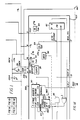
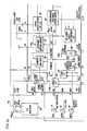
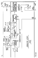
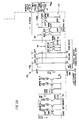
- Figs. 1a-1d comprise is a block schematic diagram of an electronic controller for a water purifying unit; and
- Figs. 2a-2d comprise is an electrical circuit diagram of an analog chip used in the electronic controller of Figs. 1a-1d.
- With reference to Fig. 1 of the drawings, the
electronic controller 100 of the present invention is comprised of ananalog chip 200 and adigital chip 300. The chips are application specific integrated circuits, commonly referred to as ASIC chips. In the preferred embodiment of the invention theanalog chip 200 was fabricated by the Raytheon Co. from their basic RLA 80 series die as number (RA8034) ASIC chip and thedigital chip 300 was fabricated by Texas Instruments as their CF61578 ASIC chip. - Although the preferred embodiment of the invention is disclosed in the form of ASIC chips it will be obvious to those persons that are skilled in the art that other forms of implementation may be used including discrete components.
- The
electronic controller 100 is powered by a single 9v. lithium battery 10 which because of the low current drain of the controller will provide more than one year of service before replacement is needed. - The
analog ASIC chip 200 has four principal sections:power control 20,conductivity test 30,LED drivers 40, andbias networks 50. - The
power control section 20 has two major functions; first, it is a very low drain voltage regulator for providing a constant + 5 V. to thedigital ASIC chip 300, and second it performs a switching function for turning on supply power in response to a conductivity test signal. The first function is necessary in order to keep the current drain of thedigital ASIC chip 300 to a consistently low value even when the battery is fresh. Thedigital ASIC chip 300 would have a higher current drain at voltages above 5 volts and may even be damaged by the full voltage of a fresh 9 volt battery. The second function is performed by an electronic switch that is activated by a conductivity test signal from thedigital ASIC 300 to turn on the supply power to theconductivity test 30 andbias networks 50 sections of this chip when a conductivity test is to be performed and to turn off the supply power at the end of the test. This function is necessary because theconductivity test section 30 has a large current drain (2-4 ma) and is therefore activated for only 4 seconds of each 8-minute cycle during a reservoir fill cycle. (details of this operation will be described later in the specification) Also, because of battery life considerations, it is necessary that thepower control section 20, which is on-line all the time, have a very low current drain. Thepower control section 20 additionally generates an artificial electrical ground potential Vg which is midway between the negative battery terminal potential -Vs and the switched positive battery supply voltage +Vs for a purpose to be designated hereinafter. - The
conductivity test section 30 measures the ratio of the conductivity of the purified water to the conductivity of the tap water. When this ratio rises above a selected predetermined value, the membrane or filter part of the unit is deemed to be spent and a "failed" test result is communicated to thedigital ASIC chip 300. Thedigital ASIC chip 300 will then change the "service required" status line to cause a "service required"LED 18 to flash. - The
conductivity test circuit 30 is connected to a pair ofconductivity probes circuit 32 is used to generate a 50% duty cycle square signal at 1KHz. A buffer U3 receives the 1KHz square wave signal and provides at its output a signal which is strong enough for actual pull-up and pull-down operation of acurrent pulser circuit 36 and a comparator andstrobe circuit 46. Thecurrent pulser 36 excites the probes from one common end with a 50% duty cycle, bi-directional square wave of current, so that the current will divide between the two probes exactly in proportion to their conductivities. This division is assisted by the fact that the transimpedance amplifiers U4 and U5 receive the conducted current at virtual ground summing junctions. The output signal from amplifier U4 is further amplified by amplifier U6, as it is the smaller of the two conducted currents, to be nominally equal to the larger signal when at the threshold value. Amplifier U6 at its negative input is connected to the wiper of the threshold gain adjust pot P101 whose gain setting determines the threshold value for the PASS/FAIL conductivity test. The comparator andstrobe circuit 46 compares the outputs from the transimpedance amplifier U4 and the output of transimpedance amplifier U5 which has been amplified by amplifier U6 to provide an output indicative of the difference between the two inputs, if any. The output signal from the comparator andstrobe circuit 46, after filtering by the low-pass filter and dischargecurrent sink 48, is used to activateswitch 54, via a comparator U8. Theswitch 54 provides the test result signal to thedigital ASIC chip 300 by clamping to the potential - Vs if the test is passed OK and to a high impedance if the test is failed. - The
LED Drivers section 40 provides for the constant current control of theLED indicators drivers LED strobe circuit 28. The LED's are enabled to turn on for 15ms of every 2 seconds during the time that a pressure switch (PS1) is closed and that a status line such as fill or service request is activated and the LED strobe signal is received. It is the LED "strobe" signal that is received from the digital ASIC via thestrobe circuit 28 which pulls down to -Vs to actually complete the turn on of the LED's. When the LED "strobe" is not pulled down to -Vs, the entireLED driver section 50 turns OFF so that there is no current drain. The constant current drive is necessary so that there will not be excessive current drain to the LED's when the battery is fresh. Also each LED (constant current) driver is set to provide a particular level of current drive according to the color of the attached LED; 0.8ma for red, 1.3ma for green, and 2.8ma for yellow. The red LED flashes when service is required, that is, the filter is dirty and should be replaced. The green LED flashes when a reservoir pressure switch PS2 is closed indicating that the reservoir is filling with purified water. The yellow LED flashes when the tap or feed water inlet pressure switch PS1 is open indicating that the tap water is under low or no pressure. - The
bias networks section 50 is activated when the conductivity test comes ON to provide bias current to all of the amplifiers, U1 through U8, in the analog ASIC chip 200 (shown in Fig. 2). The prior description has been related to the system in general and specifically to the function of the major sections of theanalog ASIC chip 200. The following description will be directed to a detailed circuit level description of theanalog ASIC chip 200 made with references to the circuitry shown in Fig. 2 which references will be grouped under the major circuit sections used in the description of Fig.1. - This section includes the low
drain voltage regulator 52 for the supply voltage for thedigital ASIC 300 and theelectronic power switch 38 for theconductivity test circuit 30. In addition, there are bias current sources consisting of transistors Q30-Q36, which form thebias circuit 34 and the ground regulator which is based on an operational amplifier U1. - Because the battery voltage will drop from 9V to about 5V during the life of the battery, the
bias circuit 34 is designed to minimize the variation of output currents as the battery ages. This circuit, is a multiple-output current mirror, with one of the outputs, Q33 and Q34 being a 2x current output by virtue of paralleling two transistors of the same die size as used for transistors Q35 and Q36. The current sources work from an input reference voltage consisting of two Vbe drops below +Vbat that occurs in transistors Q30 and Q31. The Vbe drop of transistor Q32 will offset the Vbe drop in Q30 thus leaving a net reference of one Vbe drop from Q31. The input current to the multiple output mirror then is determined by one Vbe drop divided by the resistance of R25 which is approximately 2.3 ua. Transistors Q33 and Q34, being in parallel will source about 2 x 2.3 ua which equates to 4.6 ua, but Q35 and Q36 will each mirror the 2.3 ua input current. Due to variations in +Vbat the current to Q30 and Q31 will vary considerably as the battery ages, but the source currents from Q32-Q36 will vary only slightly with battery life since the mirror input current is determined by R25 and one Vbe drop which will change only slightly with the input current to Q30 and Q31. The 4.6ua output current is used to bias the voltage regulator reference circuit and the 2.3ua output current of Q35 is used as a pull up on the TEST CONDUCTIVITY input from thedigital ASIC 300. Because that pull up source connects to the base of Q41, the TEST CONDUCTIVITY input can never pull up to more than Q41′s Vbe so thedigital ASIC 300 TEST CONDUCTIVITY output will never be exposed to the full +Vbat. The external 1.2M resistor R101 is used because there are no high value resistors available on the ASIC dies. - The
voltage regulator 52 is a simple emitter follower regulator using Q42 as a series pass transistor. The reference voltage at the base of Q42 is developed with a Vbe multiplier consisting of Q43, R28, and R102. When the voltage across R28 allows Q43 to turn ON, Vce will be clamped and further increases will just turn Q43 on harder through the resistive voltage divider, thereby shunting more of the available 4.6ua of bias current coming from current source Q33 and Q34. R102 is external because of its high value and to allow programming the clamp level of the Vbe multiplier, thereby setting the regulator output voltage. - The power switch for the conductivity test uses three NPNS transistors in parallel Q37-39 which are driven by a PNPS transistor Q40. Current source Q36 to the base of Q40 and resistor R27 from the base to emitter of Q37-39 assures complete turnoff when the switch is open. The switch will close whenever the signal on the TEST CONDUCTIVITY line is high (impedance) and the 2.3ua bias current from Q35 has turned on Q41 which in turn turns on Q40 and Q37-Q39. The output +Vs at the emitters of Q37-Q39 will be a few tenths of a volt below +Vbat.
- Since the conductivity test circuits are set up for split supplies, the
ground regulator 42 is configured to force the mid-point voltage between +Vs and -Vs to be at ground potential. The mid-point is determined by the voltage divider of R32 and R33 whose common node feeds the + input of the operational amplifier U1. It should be noted that the battery terminal voltages are otherwise free to float with respect to ground except for the action of the ground regulator which is active only during the conductivity test. Furthermore, the -Vs terminal is the common supply point between theanalog ASIC chip 200 and thedigital ASIC chip 300 and therefore the digital ASIC power is essentially floating with respect to ground most of the time. - The purpose of this section is to periodically test the conductivity of the incoming (dirty) and processed (purified) water, and to enable the
LED 18 when the processed water conductivity exceeds 25% or other selected threshold percentage of the incoming water conductivity. Besides low battery drain, two other considerations influenced this design. - First, the conductivity of the incoming water as indicated by the resistance of
probe 64, ranges from 476 ohms to 25K ohms, a ratio of over 50:1. If the signals to be compared for ratio were to each have a 50:1 range, then it would be difficult to maintain good gain accuracy for the small signals in the presence of voltage offsets and offset bias currents in the operational amplifier stages. Therefore, theprobes - Secondly, d.c. current should not be allowed to flow in
probes - The test chain begins with a 2KHz oscillator which includes U2,C101, and R1-R3. A small positive feedback voltage is provided by the voltage divider R3 and R1. Negative feedback voltage is provided through R2 but is delayed by the charging or discharging of C101. Because of this delay the output of U2 is always at a supply rail trying to either charge or discharge C101, and hence the square wave oscillator action.
- When this frequency is logically divided by two, an exact 50% duty cycle at 1 KHz will result. The 2:1 frequency divider is a double rank flip-flop. The input flip-flop includes Q1,Q2 and R4,R5 and serves to route positive clock transitions to only one side of the output flip-flop at a time. The output flip-flop includes Q3,Q4 and R6-R9. Assume for the moment that in the output flip-flop Q3 is ON and Q4 is OFF - This means the base of Q4 and hence the emitter of Q2 is at a lower voltage than the base of Q3 and the emitter of Q1 so when a positive clock transition feeds through R4 and R5 towards the input flip-flop, Q2 will begin to turn ON first. As soon as Q2 starts to turn ON, the base voltage of Q1 will be lowered thus keeping Q1 OFF as long as the clock input remains high. Since Q2 has turned ON, a positive voltage will feed through to the base of Q4 to turn on Q4, thus changing the state of the output flip-flop. When the clock goes low nothing will change, and then at the next positive clock transition a similar action takes place except that Q1 and then Q3 will turn ON thus changing the state of the output flip-flop again. The output of the divider is taken from the collector of Q4 through isolation resistor R10 to the buffer U3.
- The buffer U3 is a comparator formed from an operational amplifier so that the output will have active pull up and pull down capability with which to feed the
current pulser 36. - The
current pulser 36 is a pair of programmable current sources each with an additional resistor R13 and R14 connected between the base and the emitter circuit common of the output transistors Q7 and Q10 to assure complete and rapid turnoff as the opposite side of Q7 and Q10, respectively, turns ON. For the positive current source comprising Q5-Q7 and R11, R13 and R15, the net reference voltage is Vbe of Q5 so the output current at the collector of Q7 will be about 120ua.
- The negative current source is complementary to the positive current pulser except that the net reference comes from Vbe of Q9, which is an NPNS transistor as was Q5 in the positive pulser. The negative current source is comprised of Q8-Q10 and R12, R14 and R16. Thus the reference voltage, for each polarity pulser, comes from the same transistor type working at the same current level so the current magnitudes of the two polarities do match closely.
- If the current pulser output, at the junction of the collectors of Q7 and Q10, were connected only to the probes' coupling capacitor C102, then a slight imbalance between positive and negative current pulses would eventually cause a d.c. charge to build up on C102 until one of the current pulsers had insufficient voltage headroom to inject 120ua through the probes. Therefore, external resistor R105 is connected to ground from the pulser output to slowly bleed off any charge accumulating on C2.
- The injected current passes through
probes - The worst error condition occurs for highly conductive (very dirty) water because the driving voltage developed by the
current pulser 36 will be quite low. Under these circumstances the probe resistances would be about 500 and 2000 ohms giving an equivalent parallel resistance of 400 ohms through which the 120ua has to be driven. The driving voltage would then be 120 ua x 400 ohms = 48mv, and if the summing junctions are 1mv apart, as noted above, then the error will be 1/48 = 2.1%. - In order to detect the threshold, the 240mv "clean"
probe 62 signal at the output of U4 is amplified until at threshold it would nominally match the 960mv "dirty"probe 64 signal and could be monitored by a comparator. That gain is provided by operational amplifier U6 which is adjusted to have a nominal gain of 4 through potentiometer P101. If a threshold different from 25% is desired, then the potentiometer P101 can be adjusted to give a different gain and hence equivalent threshold. For the nominal case:
- Next the two signals are compared by a comparator U7 whose open collector transistor output is pulled up by R19. Because the probes are being pulsed with both current polarities to avoid electrolysis, the sense of the comparator output will reverse between the two pulse polarities. It is therefore, necessary to suppress the comparator output when it has the unwanted polarity. This is accomplished by Q11 which shorts the comparator output to the -Vs rail while the negative current pulse is being applied to the probes.
- During the positive current pulse the comparator inputs will both be negative, and if the amplified "clean" signal at the output of U6 is smaller than the "dirty" signal, the comparator output will pulse positive indicating an OK condition. Otherwise, the comparator output will remain negative, near -Vs rail, indicating a failed or dirty filter condition. Positive pulses, indicative of an OK condition, are rectified by the base-emitter junction of Q12 to charge the low-pass RC filter of R22 and C103. If the voltage on C103 remains positive, then the filter is OK. The 4.5ua discharge current from Q29, a constant current sink, will bleed down C103 towards -Vs if the test starts to fail. The current sink is used to avoid another high value external resistor. When the battery is fresh, Q12 may "zener" slightly between positive pulses from the comparator U7 but, nonetheless the voltage on C103 will remain positive at about +6.5V above -Vs. So if the voltage on C103 is positive the filter is OK, otherwise the voltage on C103 is negative for a failed condition.
- Comparator U8 monitors the voltage on C103 to provide a positive output if the filter is OK or otherwise to clamp to -Vs for a failed condition. This output drives Q13 which then clamps the signal on the TEST RESULT output line to -Vs, for an OK condition or goes to high impedance to indicate a failed condition. The signal on the TEST RESULT output line goes to the
digital ASIC chip 300 for storage during the time between conductivity tests and the most recent stored test result is returned as a signal on the SERVICE REQUIRED line to theLED drivers 40. - This section has two major parts; the strobe/status
current mirror 28, and the LED driver gain mirrors 22, 24 and 26. Thecurrent mirror 28 turns the whole section ON, from a zero current drain standby condition, between flashes of the LED's. Thecurrent mirror 28 also provides input current sources to the LED driver gain mirrors. Any status input line which is pulled down to -Vs by the status input from the digital ASIC will shunt away the bias or pull up input current that would otherwise feed the driver gain mirror thereby preventing the attached LED from being turned ON. Thus the LED's whose status inputs from the digital ASIC are at a HI impedance are enabled to flash ON when the LED strobe pulls low through R106. Between flashes the input current mirror shuts OFF to minimize battery drain. - The driver gain mirrors rely for current gain upon the approximately 40x ratio of emitter areas between the NPNL output transistor and the NPNS transistors on the input side. Since these transistors are all on the same die the current gain versus Vbe characteristics will all closely match on a per unit emitter area basis. Each gain mirror will have a nominal current gain equal to the ratio of output emitter area to input emitter area. If more than one NPNS transistor is used on the input side, then the mirror gain will be reduced because that ratio of output area to (now larger) input area will be reduced. Since these LED drivers are acting as constant current regulators, only a specified amount of current can reach each LED according to its color, regardless of the magnitude of +Vbat which will drop from 9V to 5V as the battery ages. Without current regulation, the LED current would have to be specified for the low, end of life value of +Vbat with the result that higher currents would flow when the battery was fresh, thereby accelerating battery aging during the first few months of service.
- The
current mirror 28 is comprised of transistors Q14-Q17 and external resistor R106. It is a conventional current mirror which relies on the matching of transistor characteristics, particularly Vbe vs Ib and current gain, to affect multiple current sources whose current output closely matches the input current. R106 will set the collector current of Q14 at about 70ua when the signal on the LED STROBE line goes active low. This will allow the collectors of Q15-Q17 to each source an approximately equal 70ua. Note that the emitters of Q14-Q17 are tied to +Vr, the regulated digital ASIC supply voltage. This is to prevent drawing any current in the mirror when the LED STROBE signal is high (at +Vr which is less than +Vbat) and to avoid over voltage on theLED strobe divider 90 on the digital ASIC chip. Each output current from the mirror, at the collectors of Q15-Q17, is a pull up source for a status input line and if not shunted to -Vs by the status input line, will feed an output gain mirror as described above whose gain is determined by emitter area ratios as follows:


Since thecurrent mirror 28 delivers about 70 ua at its outputs, the current drawn through the LED's is thus:


- Note that the output currents for all the LED's are scaled from the LED strobe current which depends on +Vr and R106. If it is desired to adjust display brightness one can simply change R106 which will now set a new input mirror current at Q14 collector then all the LED currents will scale together but in the same ratio as before so that the apparent visual brightnesses of the LED's will track together.
- This section includes various constant current sinks to the -Vs rail as required by other circuits on the chip. There are four mirror circuits in this section. They receive input current through resistors R34, R35 and R36 tied to the node joining R29 and R30 which node is intended to operate at Vbe + 1 volt = 1.6 volts above -Vs.
- Consider first the
MNIM networks # 1, #2, and #3. These networks are connected via their labeled outputs to like labeled bias inputs of the operational amplifiers and comparators.MNIM # 3 is the simplest network being a conventional NPN current mirror. R36 will have 1 volt across it so 20ua will flow into the mirror. Because there are two input transistors in parallel each transistor will be sinking 10ua individually. Since the transistors in the network all match for gain and Vbe vs Ic, and since the outputs G and H are derived from single transistors they will each sink an identical 10ua. -
MNIM # 2 looks similar toMNIM # 3, except that the input current through R35 will flow through a single transistor and will amount to 1 volt/50K = 20ua. Outputs D and E will each mirror the 20ua input current, but the transistor for output F has an emitter resistor R39 which will cause output F to sink less current than the other transistors in that network. The value of R39 is determined by first calculating the reduction in Vbe for that transistor and finding the resistor which will drop that much voltage for the new desired value of sink current. For example if a 10ua output is desired:
- Resistor R39 must then drop 18mv since Vbe for the F transistor is now reduced so:

which is close to the 1.7K value specified. -
MNIM # 1 is the same asMNIM # 2 except that the two outputs A and C are reduced to 10ua. - The current mirror of Q27 - Q29 serves two purposes: first to provide a discharge current sink for C103 and second to partially stabilize the node joining R29 and R30 against variations in voltage between -Vs and +Vs. Because there are two Vbe's (Q27 and Q28) on the input side and because the node joining R29 and R30 is intended to be at 1 volt +Vbe, there will only be about 1 volt + Vbe - 2Vbe = .4 volts across R30 so about 80ua will flow into the mirror. If +Vs rises, the current in R30 will rise more rapidly percentagewise than the current in R34-R36, and R31, with the result that the Q27-Q29 current mirror absorbs most of the extra current due to a rise in +Vs sending more current through R29. The value of R31 is calculated the same way as R39 was calculated above:


which is close to the 15K value specified. The sink current into Q29 will vary considerably with changes in +Vs but the magnitude of this current is not critical. R29 is chosen to allow about 130ua (the sum of the nominal mirror input currents) to flow when +Vs is 8 volts above -Vs. - With reference to Fig. 1, the
digital ASIC chip 300 generates timing and status commands which are passed on to theanalog ASIC chip 200. It also receives status inputs from the pressure switch PS2 and theanalog ASIC chip 200. The signals this chip passes to the analog ASIC chip initiate the conductivity ratio test and determine the status of the message display LED's which are lit by the analog ASIC chip. - Signal inputs of the digital ASIC chip will have either an external pull up resistor or an internal pull up current source from +Vr so that an input not otherwise connected will be at a logical high to prevent the possibility of drifting into an indeterminate logical state. The clear input for example uses an external pull up resistor R103 for this purpose. All other signal inputs use internal pull up
current sources 80, 83, 84, and 85 of under 5uA each from +Vs. These pull ups, which typically source from 1.5 to 3.2 uA depending in input terminal voltage level, also prevent the inputs from being left in a noise vulnerable high impedance state. - Outputs from the digital ASIC chip in a low state will have no more than 200 ohms resistance to the -Vs supply with an offset of less than +500mv. Outputs in the high state will be high impedance with leakage or source currents of less than +/- 1ua for applied voltages between -Vs and +Vr.
- The clock circuit includes an external RC network and a gain transistor feeding an on-clip MOS buffer and open-drain FET. This configuration is necessary because the available standard cell oscillator draws several hundred microamps while oscillating, which is not acceptable under our power requirements specification. With the available standard cell oscillator, the voltage at the node joining R104 and C104 feeds the on-chip buffer which then discharges C104 when the input to the oscillator block rises above the input device threshold. This mode of operation for the standard cell oscillator puts the input device in its linear range virtually all the time under which conditions the oscillator draws the large current noted.
- The oscillator configuration shown uses an external common emitter pain transistor, Q1, with its base connected to the node joining R104 and C104 and the collector feeding the on-chip buffer. In this arrangement Q1 will not turn ON until the voltage at the base rises to about 0.6V, then when it does turn ON, the collector voltage will fall very rapidly owing to the transistor voltage gain. This rapidly falling collector voltage quickly pulls down the input to the on-chip buffer taking it very quickly through the linear region so that high current is drawn only momentarily as the output open FET now discharges C104 to -Vs. Reset capacitor C105 holds the input to the on-chip buffer LOW long enough for C104 to be discharged before the buffer input again sees a HI level which soon occurs as the on-chip 5uA pull up current source charges up C105. The charge rate of C105 is fast (5uA/330pF - 15kV/sec) so that the on-chip buffer input passes through the linear region in a fraction of a millisecond. Thus the on-chip buffer input is in the linear region for only a fraction of a percent of the time so the overall current drain is reduced to an acceptably low value of about 20uA when the oscillator runs at 66Hz.
- The other part of the on-chip clock circuit is a toggle flip-flop so that its output will be a 50% duty cycle at 33Hz. A half cycle of this output takes 15.1ms and is used to gate the LED-STROBE output signal.
- The 7-
stage divider chain 90 runs continuously to provide a low duty cycle LED STROBE signal which is low for about 15ms once every 2 seconds and which is hi the rest of the time. This strobe signal allows the analog ASIC to flash the LED indicators for this same 15ms according to the status outputs connected from the digital ASIC to enable inputs on the analog ASIC. - A second 7-
stage divider 94 is provided to initiate a water conductivity test for 4 seconds at the end of every 8 minutes of elapsed time while the reservoir is filling. An 8 minute delay is built into the system to compensate for temperature changes. The input to this 7-stage divider chain is normally taken via the normal output of multiplexer switch ES1 from the (÷ 128) output of thedivider chain 90. A second 2-stage divider 92 is part of this section and normally receives its input via ES2 from the 5th stage (÷ 32) output of thedivider chain 90. The 2-stage divider 92 and thedivider chain 90 together feed an ANDgate 96 to create a COPY pulse to clock TEST RESULT data from the analog ASIC into a test memory flip-flop 82 during the 4th second of the conductivity test. This delay provides an opportunity for the initial transient responses to settle down. An input from pressure switch PS2 will be hi while not filling and under these conditions theconductivity test divider 94 and the test result memory flip-flop 82 will be held reset. Once PS2 goes low, indicating the reservoir is filling, thedivider 94 will be enabled to count 8 minute cycles for as long as PS2 is low. At the end of each 8 minute cycle a TEST CONDUCTIVITY output command is asserted for 4 seconds. - The test memory flip-
flop 82 receives the TEST RESULT input signal from the analog ASIC and at the start of the 4th second of the test using the COPY pulse generated in thetest divider 94 as described above this test result is copied into the flip-flop. The output of this flip-flop provides the SERVICE REQUIRED status output signal to allow the analog ASIC to flash the red "service required" LED if the most recent conductivity test failed and the reservoir is still filling. These 8 minute cycles continue one after another for as long as the reservoir is filling as indicated by PS2 remaining closed. Once PS2 opens, the conductivity test memory flip-flop 82 and theconductivity test divider 94 are reset and held there. - A (speedup)
multiplexer 86 incorporates electronic switches ES1 and ES2 to allow the functions of the testconductivity divider chain 94 to be sped up for chip testing and system adjustment. When the electronic switches are in the FAST position, thetest conductivity divider 94 takes its input directly from the clock via ES2. Since this effectively bypasses the 5 stages of the 7-stage divider 92 that normally separates theclock 88 and the 2-stage divider 92 in the test conductivity chain, sequences are speeded up by a factor of 32. The Electronic switch ES1 connects the 7-stage divider 90 in the test conductivity divider chain to the output of the 2-stage divider 92 to complete a 32x speedup of the entire test conductivity divider chain. - Three status outputs for the yellow "no pressure," green "filling" and red "service required." LED's enable the analog ASIC to flash those LED's whose status outputs from the digital ASIC are at a high impedance when the LED strobe signal goes low. The TEST CONDUCTIVITY output is low for 8 minutes, then high (impedance) for the 4 seconds′ duration of the test.
- The PS2 input is inverted high to low and low to high at the "FILLING" status output so that a flashing green LED will indicate a closed status of PS2 and hence a reservoir fill cycle in process. An open or high state of PS2 will also hold at reset, the conductivity test divider, and the conductivity test memory flip-flop.
Claims (18)
- An electronic controller (100) adapted for a water purifying unit of the type having a tap water inlet, a purified water outlet, a reservoir, a filter interposed between the water inlet and outlet through which the tap water passes for purification, a first conductivity probe (64) in the tap water for sensing the salinity of the tap water, and a second conductivity probe (62) in the purified water for sensing the salinity of the purified water, the first and second conductivity probes having a common input, said electronic controller being characterized by :
a current source (36) coupled to the first and second conductivity probes (64, 62) for intermittently applying a current pulse thereto resulting in current signals from the probes in the ratio of the relative conductivities (salinity) of the water samples in which they are immersed; and
electrical converting means (U4, U5) for developing voltages indicative of probe currents ; and
voltage amplifying means (U6) to cause the voltage due to current in the second probe to be just equal to the voltage due to current in the first probe when the filter has just deteriorated to the point where it should be replaced ; and
electrical comparing means (46) for comparing the voltage output signals from the first and second conductivity probe circuits (64, 62) and for generating a positive output voltage when the voltage output signal from the first conductivity probe (64) exceeds the voltage output signal from the second conductivity probe circuit (62) indicating that the filter is all right, and for generating a negative output voltage when the voltage output signal from the first conductivity probe circuit (64) is below the voltage output signal from the second conductivity probe circuit (62) for indicating that the filter should be replaced ;
electrical switching means responsive to an input from the comparing means to clamp an output line to the negative supply rail in response to a positive input and to assume a high impedance state in response to a negative input indicative of a filter in need of replacement. - An electronic controller (100) according to claim 1 wherein the converting means (U4, U5) comprises : a pair of first and second amplifiers (U4, U5), with the current output signal from the first conductivity probe (64) being fed into one of the first and second amplifiers and the current output signal from the second conductivity probe (62) being fed into the other of the first and second amplifiers.
- An electronic controller (100) according to claim 2 wherein the means for amplifying the voltage output signal from the second conductivity probe comprises a third amplifier (U6).
- An electronic controller (100) according to claim 3 wherein the electrical comparing means (46) comprises a comparator (U7) for comparing the voltage output signals from one (U5) of the first and second amplifiers and the third amplifier (U6).
- An electronic controller (100) according to claim 4 wherein the current pulses applied to the first and second conductivity probes (64, 62) have negative and positive polarities, and wherein means (Q11) are provided coupled to the comparator (U7) for shorting the comparator while the negative polarities are applied to the comparator (U7).
- An electronic controller (100) according to claim 5 wherein the shorting means for the comparator (U7) comprises a transistor (Q11).
- An electronic controller (100) according to claim 6 wherein a second transistor (Q12) is provided coupled to the comparator (U7) for rectifying the positive polarities, and wherein a capacitor (C103) is coupled to the second transistor (Q12) and is positively charged by the rectified positive polarities.
- An electronic controller (100) according to claim 7 wherein a second comparator (U8) is provided coupled to the second transistor (Q12) and the capacitor (C103) for monitoring the charge on the capacitor (C103) and generating a positive output as long as the capacitor (C103) is positively charged indicating that the filter is all tight, and generating a negative output when the capacitor (C103) is discharged indicating that the filter is dirty and should be replaced.
- An electronic controller (100) according to claim 8 wherein a third transistor (Q13) is coupled to the output of the second comparator (U8) for generating a low impedance by clamping the output ground when the filter is all right, and generating a high impedance when the filter is dirty and should be replaced.
- An electronic controller (100) according to claim 9 wherein an electronic storing and command means (300) is provided, and the output from the third transistor (Q13) is fed into the storing means (300).
- An electronic controller (100) according to claim 10 wherein the electronic storing and command means (300) generates a four-second signal every 8 minutes which is fed into the electrical current source means (36).
- An electronic controller (100) according to claim 11 wherein the electronic storing and command means (300) generates a limited time window within which the output from the third transistor (Q13) is sampled and a service required status signal is generated.
- An electronic controller (100) according to claim 12, and further comprising indicating means (18, 26) responsive to the electronic storing and command means (300) and to the service required status signal for intermittently indicating that the filter is dirty and should be replaced.
- An electronic controller (100) according to claim 13 wherein the indicating means comprises a light-emitting diode (18), and an oscillator circuit (90) electrically coupling the electronic storing and command means (300) to the light-emitting diode (18) for actuating the light-emitting diode (18) with a short pulse of several milliseconds duration every 2 seconds.
- The electronic controller (100) according to claim 14 wherein the purified water outlet means has a first normally open pressure switch (PS2) that closes when the reservoir is filling, and the tap water inlet means has a second normally open pressure switch (PS1) that closes when the tap water is under sufficient input pressure, and the oscillator circuit (90) is coupled with the light-emitting diode (18) only when the first pressure switch (PS2) is closed.
- The electronic controller (100) according to claim 15 wherein the electronic storing and command means (300) and said first pressure switch (PS2) cooperate to give a limited time window of one second for every eight minutes in which the output signal from the third transistor (Q13) is monitored to indicate whether the filter should be replaced.
- The electronic controller (100) according to claim 16 wherein the time window allows the filling cycle to commence for several minutes before any output signal from the third transistor (Q13) is monitored to allow the conductivity probes (64, 62) to reach equilibrium temperature before such monitoring, and to avoid initial overshooting of the signal.
- The electronic controller (100) according to claim 17, and further comprising a power supply (20) including a battery (10) and a common ground regulator (52) for providing a common ground potential midway between the positive battery potential and the negative battery potential so that the electronic controller (100) is insensitive to a drop in battery voltage of about one-third.
Applications Claiming Priority (3)
| Application Number | Priority Date | Filing Date | Title |
|---|---|---|---|
| US176584 | 1988-04-01 | ||
| US07/176,584 US4851818A (en) | 1988-04-01 | 1988-04-01 | Electronic controller for a water purifying unit |
| PCT/US1989/001175 WO1989009436A1 (en) | 1988-04-01 | 1989-03-23 | An electronic controller for a water purifying unit |
Publications (2)
| Publication Number | Publication Date |
|---|---|
| EP0364542A1 EP0364542A1 (en) | 1990-04-25 |
| EP0364542B1 true EP0364542B1 (en) | 1995-01-11 |
Family
ID=22644952
Family Applications (1)
| Application Number | Title | Priority Date | Filing Date |
|---|---|---|---|
| EP89903884A Expired - Lifetime EP0364542B1 (en) | 1988-04-01 | 1989-03-23 | An electronic controller for a water purifying unit |
Country Status (8)
| Country | Link |
|---|---|
| US (1) | US4851818A (en) |
| EP (1) | EP0364542B1 (en) |
| JP (1) | JPH02503830A (en) |
| AU (1) | AU605039B2 (en) |
| BR (1) | BR8906484A (en) |
| CA (1) | CA1316578C (en) |
| MX (1) | MX163512B (en) |
| WO (1) | WO1989009436A1 (en) |
Cited By (2)
| Publication number | Priority date | Publication date | Assignee | Title |
|---|---|---|---|---|
| EP2819426B1 (en) | 2003-07-28 | 2017-12-27 | Deka Products Limited Partnership | Systems and methods for water purification |
| US10913662B2 (en) | 2002-11-13 | 2021-02-09 | Deka Products Limited Partnership | Systems and methods for distributed utilities |
Families Citing this family (42)
| Publication number | Priority date | Publication date | Assignee | Title |
|---|---|---|---|---|
| EP0446365A4 (en) * | 1989-09-29 | 1992-07-08 | Inax Corporation | Water discharging apparatus |
| US5145575A (en) * | 1990-03-09 | 1992-09-08 | Burrows Bruce D | Water quality monitor for a water purification system |
| US5057212A (en) | 1990-03-09 | 1991-10-15 | Burrows Bruce D | Water conductivity monitor and circuit with extended operating life |
| JP2772365B2 (en) | 1990-06-05 | 1998-07-02 | オルガノ株式会社 | Water quality monitor |
| US5112477A (en) * | 1991-03-01 | 1992-05-12 | Hamlin Jerry J | Purified water and ice dispensing apparatus |
| US5450358A (en) * | 1991-09-30 | 1995-09-12 | Mckesson Corporation | Method and system for monitoring the quality of a water purification apparatus |
| JPH0580585U (en) * | 1991-12-03 | 1993-11-02 | 株式会社オニック | Desalination equipment |
| US5298851A (en) * | 1992-05-12 | 1994-03-29 | Transpo Electronics, Inc. | Multiple application voltage regulator system and method |
| US5328597A (en) * | 1992-07-27 | 1994-07-12 | The Clorox Corporation | Electronic monitoring unit for monitoring number of uses of cartridge |
| US5434561A (en) * | 1993-11-09 | 1995-07-18 | Master Hydrosystems, Inc. | Remote audio/visual alarm apparatus |
| US5494573A (en) * | 1994-02-14 | 1996-02-27 | Aquatec Water Systems, Inc. | Reverse osmosis water purification diagnostic system |
| US5580444A (en) * | 1994-03-14 | 1996-12-03 | Hydrotechnology, Inc. | Water quality monitor for a water purification system |
| US5435909A (en) * | 1994-03-14 | 1995-07-25 | Hydrotechnology, Inc. A California Corp. | Water quality monitor for a water purification system |
| US6217751B1 (en) | 1995-01-23 | 2001-04-17 | Aquatec Water Systems, Inc. | Water quality monitor for a reverse osmosis water purification system |
| SE503918C2 (en) * | 1995-01-31 | 1996-09-30 | Electrolux Ab | Apparatus for purifying water comprising a pressurized membrane chamber and a method for determining the flushing time of a pressurized membrane chamber |
| US5820765A (en) * | 1996-04-17 | 1998-10-13 | Samsung Electronics Co., Ltd. | Apparatus and method for displaying the purifying efficiency of the water purifier |
| US6186140B1 (en) | 1997-03-14 | 2001-02-13 | 3M Innovative Properties Company | Respiratory filter element having a storage device for keeping track of filter usage and a system for use therewith |
| US6673250B2 (en) * | 1999-06-21 | 2004-01-06 | Access Business Group International Llc | Radio frequency identification system for a fluid treatment system |
| US6306290B1 (en) * | 2000-06-26 | 2001-10-23 | Patrick J. Rolfes | Water filter replacement indicator |
| US20050134119A1 (en) * | 2003-12-18 | 2005-06-23 | Bliley Paul D. | Time slotting power switching |
| US7408527B2 (en) * | 2004-04-30 | 2008-08-05 | Infocus Corporation | Light emitting device driving method and projection apparatus so equipped |
| US20060144765A1 (en) * | 2004-12-30 | 2006-07-06 | Timothy Skwiot | Conductivity measurement and monitoring system for a fluid treatment system |
| CA2771265C (en) * | 2005-01-27 | 2014-05-06 | Ecowater Systems, Llc | Encapsulated water treatment system |
| US8395476B2 (en) * | 2005-06-09 | 2013-03-12 | Whirlpool Corporation | Consumable holder with taxonomy |
| US8442042B2 (en) * | 2005-06-09 | 2013-05-14 | Whirlpool Corporation | Appliance and a consumable holder with an embedded virtual router |
| US8477007B2 (en) * | 2005-06-09 | 2013-07-02 | Whirlpool Corporation | Appliance and a consumable holder in a network |
| US8314678B2 (en) * | 2005-06-09 | 2012-11-20 | Whirlpool Corporation | Consumable holder with a cycle structure for an appliance |
| US20090040066A1 (en) * | 2005-06-09 | 2009-02-12 | Whirlpool Corporation | Consumable holder with routable data packet for an appliance |
| US20090044137A1 (en) * | 2005-06-09 | 2009-02-12 | Whirlpool Corporation | Consumable holder with user interface data |
| US20090044129A1 (en) * | 2005-06-09 | 2009-02-12 | Whirlpool Corporation | Graphical user interface to control interactions between an appliance and a consumable holder |
| US8264318B2 (en) * | 2005-06-09 | 2012-09-11 | Whirlpool Corporation | Consumable holder with converter |
| US7388509B2 (en) * | 2005-09-28 | 2008-06-17 | International Lubricants, Inc. | System and method for detecting electrolysis in an automobile system |
| US7759948B2 (en) * | 2007-10-05 | 2010-07-20 | Pentair Filtration Solutions, Llc | Disposable total dissolved solids meter and methods of use thereof |
| US8118997B2 (en) * | 2008-10-23 | 2012-02-21 | Whirlpool Corporation | Smart filter for an appliance |
| US20100102051A1 (en) * | 2008-10-23 | 2010-04-29 | Whirlpool Corporation | Consumable holder with electronics to communicate with an appliance |
| US8010211B2 (en) * | 2008-10-23 | 2011-08-30 | Whirlpool Corporation | Appliance with a service interface for communicating with a consumable holder |
| US20100125364A1 (en) * | 2008-11-20 | 2010-05-20 | Whirlpool Corporation | Configurable consumable holder for an appliance |
| US8461959B2 (en) * | 2008-10-23 | 2013-06-11 | Whirlpool Corporation | Consumable holder with process control apparatus |
| TWI481151B (en) * | 2011-08-10 | 2015-04-11 | 創傑科技股份有限公司 | Battery powered device with integrated power management and charging unit circuitry |
| US9116099B2 (en) * | 2012-12-27 | 2015-08-25 | General Electric Company | Wide dynamic range conductivity measurements in water |
| US11453989B2 (en) * | 2018-10-10 | 2022-09-27 | Remora Incorporated | Hybrid water filtering cleaning and quality monitoring device |
| US20200115868A1 (en) * | 2018-10-10 | 2020-04-16 | Remora Incorporated | Hybrid water filtering cleaning and quality monitoring device |
Citations (3)
| Publication number | Priority date | Publication date | Assignee | Title |
|---|---|---|---|---|
| US3838774A (en) * | 1973-01-02 | 1974-10-01 | N Ball | Apparatus for monitoring water purification system |
| US3990066A (en) * | 1974-10-25 | 1976-11-02 | Malmgren Arthur L | Water quality monitor |
| US4587518A (en) * | 1982-11-08 | 1986-05-06 | Baxter Travenol Laboratories, Inc. | Monitor and control system for water purification apparatus |
Family Cites Families (2)
| Publication number | Priority date | Publication date | Assignee | Title |
|---|---|---|---|---|
| JPS4935270U (en) * | 1972-06-30 | 1974-03-28 | ||
| US3869382A (en) * | 1974-01-03 | 1975-03-04 | Vast Associates Inc J | Method and apparatus for determining exhaustion of a mass of ion exchange material and a device using the same |
-
1988
- 1988-04-01 US US07/176,584 patent/US4851818A/en not_active Expired - Fee Related
-
1989
- 1989-03-21 CA CA000594276A patent/CA1316578C/en not_active Expired - Fee Related
- 1989-03-23 WO PCT/US1989/001175 patent/WO1989009436A1/en not_active Ceased
- 1989-03-23 BR BR898906484A patent/BR8906484A/en unknown
- 1989-03-23 EP EP89903884A patent/EP0364542B1/en not_active Expired - Lifetime
- 1989-03-23 JP JP1504016A patent/JPH02503830A/en active Pending
- 1989-03-23 AU AU34364/89A patent/AU605039B2/en not_active Ceased
- 1989-03-31 MX MX15488A patent/MX163512B/en unknown
Patent Citations (3)
| Publication number | Priority date | Publication date | Assignee | Title |
|---|---|---|---|---|
| US3838774A (en) * | 1973-01-02 | 1974-10-01 | N Ball | Apparatus for monitoring water purification system |
| US3990066A (en) * | 1974-10-25 | 1976-11-02 | Malmgren Arthur L | Water quality monitor |
| US4587518A (en) * | 1982-11-08 | 1986-05-06 | Baxter Travenol Laboratories, Inc. | Monitor and control system for water purification apparatus |
Cited By (2)
| Publication number | Priority date | Publication date | Assignee | Title |
|---|---|---|---|---|
| US10913662B2 (en) | 2002-11-13 | 2021-02-09 | Deka Products Limited Partnership | Systems and methods for distributed utilities |
| EP2819426B1 (en) | 2003-07-28 | 2017-12-27 | Deka Products Limited Partnership | Systems and methods for water purification |
Also Published As
| Publication number | Publication date |
|---|---|
| WO1989009436A1 (en) | 1989-10-05 |
| EP0364542A1 (en) | 1990-04-25 |
| JPH02503830A (en) | 1990-11-08 |
| AU3436489A (en) | 1989-10-16 |
| US4851818A (en) | 1989-07-25 |
| CA1316578C (en) | 1993-04-20 |
| BR8906484A (en) | 1990-12-04 |
| MX163512B (en) | 1992-05-25 |
| AU605039B2 (en) | 1991-01-03 |
Similar Documents
| Publication | Publication Date | Title |
|---|---|---|
| US4851818A (en) | Electronic controller for a water purifying unit | |
| US4937557A (en) | Monitoring and indicating circuit for reverse osmosis filter | |
| US4514722A (en) | Domestic automatic continuously monitoring soil moisture monitor/indicator | |
| US4849098A (en) | Continuous water quality monitor | |
| EP0083996B1 (en) | Electronic switching device with exciting coil | |
| JPS6470998A (en) | Decision circuit for use of redundant memory cell | |
| KR890008499A (en) | Solenoid valve drive control circuit | |
| US20060144765A1 (en) | Conductivity measurement and monitoring system for a fluid treatment system | |
| US4047099A (en) | Method and apparatus for determining boiler water conductivity | |
| EP0940904A2 (en) | Emergency lighting system | |
| JPH1043756A (en) | Pressurizing pump control device for water purifier | |
| US6644103B1 (en) | Method and apparatus for detecting a dry/wet state of a thermistor bead | |
| US20040080423A1 (en) | Method and apparatus for detecting a dry/wet state of a thermistor bead | |
| GB2130735A (en) | Battery testing apparatus | |
| KR890004951B1 (en) | Water level detection circuit of electrode | |
| JPH0668798B2 (en) | Gas alarm shutoff system | |
| KR940005926Y1 (en) | Solenoid valve drive control circuit | |
| KR100423656B1 (en) | watchdog circuit of ECU for vehicle | |
| SU1306759A1 (en) | Device for protection of d.c.traction drive | |
| SU1282133A1 (en) | Device for checking decoder | |
| JPH0975942A (en) | Electrolytic ionized water generator | |
| JPH0326685Y2 (en) | ||
| JPS6412056B2 (en) | ||
| JPS63103338A (en) | display device | |
| JPH0614384Y2 (en) | Latching relay drive circuit |
Legal Events
| Date | Code | Title | Description |
|---|---|---|---|
| PUAI | Public reference made under article 153(3) epc to a published international application that has entered the european phase |
Free format text: ORIGINAL CODE: 0009012 |
|
| AK | Designated contracting states |
Kind code of ref document: A1 Designated state(s): BE CH DE FR GB IT LI NL |
|
| 17P | Request for examination filed |
Effective date: 19900605 |
|
| 17Q | First examination report despatched |
Effective date: 19930118 |
|
| GRAA | (expected) grant |
Free format text: ORIGINAL CODE: 0009210 |
|
| AK | Designated contracting states |
Kind code of ref document: B1 Designated state(s): FR GB |
|
| PGFP | Annual fee paid to national office [announced via postgrant information from national office to epo] |
Ref country code: GB Payment date: 19950217 Year of fee payment: 7 |
|
| PGFP | Annual fee paid to national office [announced via postgrant information from national office to epo] |
Ref country code: FR Payment date: 19950314 Year of fee payment: 7 |
|
| ET | Fr: translation filed | ||
| PLBE | No opposition filed within time limit |
Free format text: ORIGINAL CODE: 0009261 |
|
| STAA | Information on the status of an ep patent application or granted ep patent |
Free format text: STATUS: NO OPPOSITION FILED WITHIN TIME LIMIT |
|
| 26N | No opposition filed | ||
| PG25 | Lapsed in a contracting state [announced via postgrant information from national office to epo] |
Ref country code: GB Effective date: 19960323 |
|
| GBPC | Gb: european patent ceased through non-payment of renewal fee |
Effective date: 19960323 |
|
| PG25 | Lapsed in a contracting state [announced via postgrant information from national office to epo] |
Ref country code: FR Effective date: 19961129 |
|
| REG | Reference to a national code |
Ref country code: FR Ref legal event code: ST |