EP0364448B1 - Monolithic integrated waveguide-photodiode-fet combination - Google Patents
Monolithic integrated waveguide-photodiode-fet combination Download PDFInfo
- Publication number
- EP0364448B1 EP0364448B1 EP88902790A EP88902790A EP0364448B1 EP 0364448 B1 EP0364448 B1 EP 0364448B1 EP 88902790 A EP88902790 A EP 88902790A EP 88902790 A EP88902790 A EP 88902790A EP 0364448 B1 EP0364448 B1 EP 0364448B1
- Authority
- EP
- European Patent Office
- Prior art keywords
- photodiode
- layer
- zone
- fet
- doped
- Prior art date
- Legal status (The legal status is an assumption and is not a legal conclusion. Google has not performed a legal analysis and makes no representation as to the accuracy of the status listed.)
- Expired - Lifetime
Links
- 239000000463 material Substances 0.000 claims abstract description 18
- 239000004065 semiconductor Substances 0.000 claims abstract description 14
- 239000000758 substrate Substances 0.000 claims abstract description 10
- 229910052733 gallium Inorganic materials 0.000 claims description 5
- VYPSYNLAJGMNEJ-UHFFFAOYSA-N Silicium dioxide Chemical compound O=[Si]=O VYPSYNLAJGMNEJ-UHFFFAOYSA-N 0.000 claims description 4
- 229910052782 aluminium Inorganic materials 0.000 claims description 4
- 229910052581 Si3N4 Inorganic materials 0.000 claims description 2
- PNEYBMLMFCGWSK-UHFFFAOYSA-N aluminium oxide Inorganic materials [O-2].[O-2].[O-2].[Al+3].[Al+3] PNEYBMLMFCGWSK-UHFFFAOYSA-N 0.000 claims description 2
- 229910052681 coesite Inorganic materials 0.000 claims description 2
- 229910052593 corundum Inorganic materials 0.000 claims description 2
- 229910052906 cristobalite Inorganic materials 0.000 claims description 2
- 239000000377 silicon dioxide Substances 0.000 claims description 2
- 235000012239 silicon dioxide Nutrition 0.000 claims description 2
- 229910052682 stishovite Inorganic materials 0.000 claims description 2
- 229910052905 tridymite Inorganic materials 0.000 claims description 2
- 229910001845 yogo sapphire Inorganic materials 0.000 claims description 2
- 229910000530 Gallium indium arsenide Inorganic materials 0.000 claims 1
- 239000011810 insulating material Substances 0.000 claims 1
- 230000008878 coupling Effects 0.000 abstract description 6
- 238000010168 coupling process Methods 0.000 abstract description 6
- 238000005859 coupling reaction Methods 0.000 abstract description 6
- 230000005669 field effect Effects 0.000 description 9
- 230000010354 integration Effects 0.000 description 5
- 229910052738 indium Inorganic materials 0.000 description 4
- 238000004519 manufacturing process Methods 0.000 description 4
- 230000003287 optical effect Effects 0.000 description 4
- 238000002513 implantation Methods 0.000 description 3
- 230000005855 radiation Effects 0.000 description 3
- 238000000926 separation method Methods 0.000 description 3
- XEEYBQQBJWHFJM-UHFFFAOYSA-N Iron Chemical compound [Fe] XEEYBQQBJWHFJM-UHFFFAOYSA-N 0.000 description 2
- 238000010521 absorption reaction Methods 0.000 description 2
- 238000009792 diffusion process Methods 0.000 description 2
- 239000013307 optical fiber Substances 0.000 description 2
- 238000002161 passivation Methods 0.000 description 2
- 230000000704 physical effect Effects 0.000 description 2
- 229910052785 arsenic Inorganic materials 0.000 description 1
- 230000005540 biological transmission Effects 0.000 description 1
- 238000005253 cladding Methods 0.000 description 1
- 238000004891 communication Methods 0.000 description 1
- 238000005516 engineering process Methods 0.000 description 1
- 238000005530 etching Methods 0.000 description 1
- 239000007943 implant Substances 0.000 description 1
- 238000009434 installation Methods 0.000 description 1
- 238000009413 insulation Methods 0.000 description 1
- 238000005468 ion implantation Methods 0.000 description 1
- 229910052742 iron Inorganic materials 0.000 description 1
- 238000002955 isolation Methods 0.000 description 1
- 239000002184 metal Substances 0.000 description 1
- 229910052751 metal Inorganic materials 0.000 description 1
- 230000005693 optoelectronics Effects 0.000 description 1
Images
Classifications
-
- G—PHYSICS
- G02—OPTICS
- G02B—OPTICAL ELEMENTS, SYSTEMS OR APPARATUS
- G02B6/00—Light guides; Structural details of arrangements comprising light guides and other optical elements, e.g. couplings
- G02B6/10—Light guides; Structural details of arrangements comprising light guides and other optical elements, e.g. couplings of the optical waveguide type
- G02B6/12—Light guides; Structural details of arrangements comprising light guides and other optical elements, e.g. couplings of the optical waveguide type of the integrated circuit kind
- G02B6/12004—Combinations of two or more optical elements
-
- G—PHYSICS
- G02—OPTICS
- G02B—OPTICAL ELEMENTS, SYSTEMS OR APPARATUS
- G02B6/00—Light guides; Structural details of arrangements comprising light guides and other optical elements, e.g. couplings
- G02B6/24—Coupling light guides
- G02B6/42—Coupling light guides with opto-electronic elements
-
- H—ELECTRICITY
- H01—ELECTRIC ELEMENTS
- H01L—SEMICONDUCTOR DEVICES NOT COVERED BY CLASS H10
- H01L27/00—Devices consisting of a plurality of semiconductor or other solid-state components formed in or on a common substrate
- H01L27/14—Devices consisting of a plurality of semiconductor or other solid-state components formed in or on a common substrate including semiconductor components sensitive to infrared radiation, light, electromagnetic radiation of shorter wavelength or corpuscular radiation and specially adapted either for the conversion of the energy of such radiation into electrical energy or for the control of electrical energy by such radiation
- H01L27/144—Devices controlled by radiation
- H01L27/1443—Devices controlled by radiation with at least one potential jump or surface barrier
-
- H—ELECTRICITY
- H01—ELECTRIC ELEMENTS
- H01L—SEMICONDUCTOR DEVICES NOT COVERED BY CLASS H10
- H01L31/00—Semiconductor devices sensitive to infrared radiation, light, electromagnetic radiation of shorter wavelength or corpuscular radiation and specially adapted either for the conversion of the energy of such radiation into electrical energy or for the control of electrical energy by such radiation; Processes or apparatus specially adapted for the manufacture or treatment thereof or of parts thereof; Details thereof
- H01L31/08—Semiconductor devices sensitive to infrared radiation, light, electromagnetic radiation of shorter wavelength or corpuscular radiation and specially adapted either for the conversion of the energy of such radiation into electrical energy or for the control of electrical energy by such radiation; Processes or apparatus specially adapted for the manufacture or treatment thereof or of parts thereof; Details thereof in which radiation controls flow of current through the device, e.g. photoresistors
- H01L31/10—Semiconductor devices sensitive to infrared radiation, light, electromagnetic radiation of shorter wavelength or corpuscular radiation and specially adapted either for the conversion of the energy of such radiation into electrical energy or for the control of electrical energy by such radiation; Processes or apparatus specially adapted for the manufacture or treatment thereof or of parts thereof; Details thereof in which radiation controls flow of current through the device, e.g. photoresistors characterised by potential barriers, e.g. phototransistors
- H01L31/101—Devices sensitive to infrared, visible or ultraviolet radiation
- H01L31/102—Devices sensitive to infrared, visible or ultraviolet radiation characterised by only one potential barrier
- H01L31/103—Devices sensitive to infrared, visible or ultraviolet radiation characterised by only one potential barrier the potential barrier being of the PN homojunction type
- H01L31/1035—Devices sensitive to infrared, visible or ultraviolet radiation characterised by only one potential barrier the potential barrier being of the PN homojunction type the devices comprising active layers formed only by AIIIBV compounds
-
- H—ELECTRICITY
- H04—ELECTRIC COMMUNICATION TECHNIQUE
- H04B—TRANSMISSION
- H04B10/00—Transmission systems employing electromagnetic waves other than radio-waves, e.g. infrared, visible or ultraviolet light, or employing corpuscular radiation, e.g. quantum communication
- H04B10/60—Receivers
- H04B10/66—Non-coherent receivers, e.g. using direct detection
- H04B10/69—Electrical arrangements in the receiver
Definitions
- the present invention relates to a monolithically integrated photodiode-FET combination for installation in optical communication systems according to the preamble of claim 1.
- optical data transmission systems is towards using integrated opto-electronic circuits for the connection between optical and electronic components.
- the problem of the monolithic integration of optical fibers, photo detectors and preamplifiers in one component arises on the receiver side.
- Good compatibility of the semiconductor layers and technologies required for the various components and good coupling efficiency between the waveguide and the photodetector are required.
- Closed concepts for the integration of optical fibers, photodetectors and transistors are not known. Essentially three concepts have been proposed for the waveguide-photodiode combination.
- the radiation is decoupled into the photodiode by a suitable deflection of the beam direction into the photodiode.
- a suitable deflection of the beam direction into the photodiode is described, for example, in the publication DB Ostrowsky ea: "Integrated optical photodetector", Appl. Phys. Lett. 22 , 463-464 (1973).
- Deviating structures of waveguide-photodiode combinations, in which the radiation is coupled out of the waveguide by deflection, are described in patent applications EP-A-0 187 198 and EP-A-0 192 850.
- a second possibility of decoupling radiation is leakage wave coupling, which is used, for example, in the case of C. Bornholdt ea: "Waveguide-integrated PIN photodiode on InP ", Electr. Lett. 23 , 2-3 (1987) structure is realized.
- the third concept provides butt coupling. An explanation of this can be found in the publication GE Stillman ea: "Monolithic integrated In x Ga 1-x As Schottky-barrier waveguide photodetector", Appl. Phys. Lett. 25 , 36-38 (1974).
- JFET junction field-effect transistors
- MESFET metal-semiconductor field-effect transistors
- MISFET metal-insulator-semiconductor field-effect transistors
- the object of the present invention is to provide a layer structure which is as simple to manufacture as possible for the monolithic integration of waveguide, photodetector and transistor in a common component with high effectiveness.
- the semiconductor layer structure for a component according to the invention consists of a carrier substrate - preferably semi-insulating InP - on which a weakly n-doped waveguide layer is preferably doped in the areas provided for waveguide, photodiode or FET - preferably (In, Ga) (As, P) or (In, Ga, Al) As - and a weakly n-doped photodiode / FET layer - preferably (In, Ga) As -, which acts as an absorption layer for the photodiode and as Serves channel layer for the field effect transistor are applied.
- a closed weakly n-doped top layer - preferably InP or (In, Al) As - serves as a cladding layer for the waveguide and as a passivating layer for the photodiode and the field effect transistor.
- the waveguide can be designed, for example, in a strip form.
- the p-area of the photodiode is formed by p+-diffusion or p+-implantation.
- the light emerging from the waveguide is absorbed in the photodiode layer and generates the photocurrent.
- the n-contact of the photodiode is attached laterally over a first n-area.
- the main advantage of surge coupling is good coupling efficiency and a small diode area.
- the field effect transistor is separated from the photodiode by a separating region which is etched out in a trench shape or is formed by insulation implantation.
- the doping profile required for the FET is set by ion implantation.
- the strip-shaped gate consisting of the gate region in the semiconductor and the applied gate contact, is designed as a junction gate with p+ diffusion or p+ implantation or as a Schottky gate.
- the source and drain regions are heavily n-type doped and provided with source contact and drain contact.
- the configuration of the FET can correspond to one of the usual configurations.
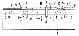
- the carrier substrate 1 made of InP material which was made semi-insulating, for example with iron doping
- a waveguide layer the made of weakly n-doped semiconductor material - z. B. 0.9 Ga 0.1 As 0.8 P 0.2 - and is usually strip-shaped, grown epitaxially and structured by etching. Adjacent to this, a likewise weakly n-doped semiconductor layer - for example, in 0.53 Ga 0.47 As material - has grown epitaxially as a photodiode layer 3 and as a FET layer 4.
- the waveguide layer 2 directly adjoins the photodiode layer 3. Waveguide layer 2, photodiode layer 3 and FET layer 4 together form a flat surface which is covered with a cover layer 5, which is InP material in the present exemplary embodiment.
- a strongly p-doped and a very strongly n-doped region are formed, which form the p-region 7 of the photodiode and the first n-region 8 of the photodiode.
- This p-region 7 and first n-region 8 are formed up to the surface of the cover layer 5 and into the photodiode layer 3.
- P-contact 14 and n-contact 15 are applied to the surface.
- a second n region 9 of the photodiode which is heavily n-conductively doped, is formed in the carrier substrate 1, as a result of which the series resistance of the photodiode is reduced.
- the very heavily n-doped source region 10 and the very heavily n-doped drain region 12 are formed in the cover layer 5 above the FET layer 4, each reaching to the surface of the cover layer 5 and as far as possible are formed far into the FET layer.
- the corresponding contacts, the source contact 16 and the drain contact 18, are applied to the surface.
- a channel region 11 with a strong n-type doping is formed, the dimension and doping profile of which are selected in accordance with the physical properties of the transistor to be achieved are.
- a corresponding gate region 13 which is heavily p-conductively doped, is formed in the cover layer 5. If a Schottky contact is used, this gate region 13 is doped n-conducting.
- the gate region 13, which is formed in the dech layer 5 up to the surface is provided with the gate contact 17 on this surface.
- a passivation layer 6 made of a dielectric is applied to the cover layer 5, insofar as it is not provided with metal contacts.
- material Si3N4, SiO2, Al2O3 or comparable materials come into question.
- the photodiode is separated from the field effect transistor by a separation region 19. This separation area 19 is designed as an etched-out trench or as an area with an isolation implant.
Landscapes
- Physics & Mathematics (AREA)
- Engineering & Computer Science (AREA)
- General Physics & Mathematics (AREA)
- Microelectronics & Electronic Packaging (AREA)
- Power Engineering (AREA)
- Electromagnetism (AREA)
- Condensed Matter Physics & Semiconductors (AREA)
- Optics & Photonics (AREA)
- Computer Hardware Design (AREA)
- Computer Networks & Wireless Communication (AREA)
- Signal Processing (AREA)
- Light Receiving Elements (AREA)
- Solid State Image Pick-Up Elements (AREA)
Abstract
Description
Die vorliegende Erfindung betrifft eine monolithisch integrierte Fotodioden-FET-Kombination zum Einbau in optische Nachrichtensysteme nach dem Oberbegriff des Anspruches 1.The present invention relates to a monolithically integrated photodiode-FET combination for installation in optical communication systems according to the preamble of
Die Entwicklung optischer Datenübertragungssysteme geht dahin, für die Verbindung zwischen optischen und elektronischen Komponenten integrierte opto-elektronische Schaltkreise einzusetzen. Auf der Empfängerseite stellt sich das Problem der monolithischen Integration von Lichtwellenleitern, Fotodetektoren und Vorverstärker in einem Bauelement. Gefordert werden gute Kompatibilität der für die verschiedenen Komponenten benötigten Halbleiterschichten und Technologien sowie ein guter Kopplungswirkungsgrad zwischen Wellenleiter und Fotodetektor. Geschlossene Konzepte zur Integration von Lichtwellenleiter, Fotodetektor und Transistor sind nicht bekannt. Für die Wellenleiter-Fotodioden -Kombination sind bisher im wesentlichen drei Konzepte vorgeschlagen worden.The development of optical data transmission systems is towards using integrated opto-electronic circuits for the connection between optical and electronic components. The problem of the monolithic integration of optical fibers, photo detectors and preamplifiers in one component arises on the receiver side. Good compatibility of the semiconductor layers and technologies required for the various components and good coupling efficiency between the waveguide and the photodetector are required. Closed concepts for the integration of optical fibers, photodetectors and transistors are not known. Essentially three concepts have been proposed for the waveguide-photodiode combination.
Die Auskopplung der Strahlung in die Fotodiode erfolgt bei dem ersten dieser Konzepte durch eine geeignete Umlenkung der Strahlrichtung in die Fotodiode. Die Realisierung einer derartigen Anordnung ist z.B. in der Druckschrift D.B. Ostrowsky e.a.: "Integrated optical photodetector", Appl. Phys. Lett. 22, 463-464 (1973) beschrieben. Davon abweichende Aufbauten von Wellenleiter-Fotodioden-Kombinationen, bei denen die Strahlung aus dem Wellenleiter durch Umlenken ausgekoppelt wird, sind in den Patentanmeldungen EP-A-0 187 198 und EP-A-0 192 850 beschrieben.In the first of these concepts, the radiation is decoupled into the photodiode by a suitable deflection of the beam direction into the photodiode. The implementation of such an arrangement is described, for example, in the publication DB Ostrowsky ea: "Integrated optical photodetector", Appl. Phys. Lett. 22 , 463-464 (1973). Deviating structures of waveguide-photodiode combinations, in which the radiation is coupled out of the waveguide by deflection, are described in patent applications EP-A-0 187 198 and EP-A-0 192 850.
Eine zweite Möglichkeit der Strahlungsauskopplung besteht in der Leckwellenkopplung, die z.B. bei dem in der Druckschrift C. Bornholdt e. a.: "Waveguide-integrated PIN photodiode on InP", Electr. Lett. 23, 2-3 (1987) angegebenen Aufbau realisiert ist.
Das dritte Konzept sieht Stoßkopplung vor. Eine Ausführung hierzu findet man in der Druckschrift G.E. Stillman e.a.: "Monolithic integrated InxGa1-xAs Schottky-barrier waveguide photodetector", Appl. Phys. Lett. 25, 36-38 (1974).A second possibility of decoupling radiation is leakage wave coupling, which is used, for example, in the case of C. Bornholdt ea: "Waveguide-integrated PIN photodiode on InP ", Electr. Lett. 23 , 2-3 (1987) structure is realized.
The third concept provides butt coupling. An explanation of this can be found in the publication GE Stillman ea: "Monolithic integrated In x Ga 1-x As Schottky-barrier waveguide photodetector", Appl. Phys. Lett. 25 , 36-38 (1974).
Zur Integration von Fododetektor und Feldeffekttransistor sind eine Reihe von Konzepten veröffentlicht, die in der Übersichtsarbeit 0. Wada, IEEE J. Quantum Electr. QE-22, 805-821 (1986) beschrieben sind und die in obenbegriff des Anspruchs 1 aufgefühnten Merkmale aufweisen (vgl. Figur 22). Der Grund für die verschiedenen Konsepte zur Integration von Fotodetecktor und Feldeffekttransistor liegt in den unterschiedlichen physikalischen Eigenschaften dieser Bauelemente, und zwar am unterschiedlichen Aufbau der Halbleiterschichten in Geometrie und Dotierung. Um trotzdem einen planaren Chipaufbau zu ermöglichen, sind vergrabene Fotodetektor-und/oder FET-Strukturen vorgeschlagen worden. Als FET-Strukturen kommen dabei Sperrschichtfeldeffekttransistoren (JFET), Metall-Halbleiter-Feldeffekttransistoren (MESFET) und Metall-Isolator-Halbleiter-Feldeffekttransistoren (MISFET) in Betracht.A number of concepts for the integration of the fododetector and field effect transistor have been published, which are described in the review article 0. Wada, IEEE J. Quantum Electr. QE-22 , 805-821 (1986) and which have the features listed in the preamble of claim 1 (cf. FIG. 22). The reason for the different concepts for the integration of photodetector and field effect transistor lies in the different physical properties of these components, namely the different structure of the semiconductor layers in geometry and doping. In order to nevertheless enable a planar chip structure, buried photodetector and / or FET structures have been proposed. In this context, junction field-effect transistors (JFET), metal-semiconductor field-effect transistors (MESFET) and metal-insulator-semiconductor field-effect transistors (MISFET) come into consideration as FET structures.
Aus der älteren europäischen Patentammeldung EP-A-0 272 372, die unter Antikel 54(3) EP ü fällt, ist bereits eine monolithisch integrierte Wellenleister/PIN-Fotodiodem/FET-kombination bekannt, bei der sich die Deckschicht nicht über die Wellenleiterschicht und der p-datierte 2. Bereich nicht in die Fotodioden schicht erstrecken.From the older European patent application EP-A-0 272 372, which falls under Article 54 (3) EP ü, a monolithically integrated waveguide / PIN-photodiode / FET combination is already known, in which the cover layer does not extend over the waveguide layer and the p-dated 2nd area does not extend into the photodiode layer.
Aufgabe der vorliegenden Erfindung ist es, einen möglichst einfach herstellbaren Schichtaufbau für die monolithische Integration von Wellenleiter, Fotodetektor und Transistor in einem gemeinsamen Bauteil mit hoher Effektivität anzugeben.The object of the present invention is to provide a layer structure which is as simple to manufacture as possible for the monolithic integration of waveguide, photodetector and transistor in a common component with high effectiveness.
Diese Aufgabe wird bei einer erfindungsgemäßen Anordnung durch die Merkmale des Anspruchs 1 gelöst.This object is achieved in an arrangement according to the invention by the features of
Die Halbleiterschichtstruktur für ein erfindungsgemäßes Bauelement besteht aus einem Trägersubstrat - vorzugsweise semiisolierendes InP - , auf das in den für Wellenleiter, Fotodiode bzw. FET vorgesehenen Bereichen durch Lokalepitaxie eine schwach n-leitend dotierte Wellenleiterschicht - vorzugsweise (In,Ga) (As,P) oder (In,Ga,Al) As - sowie eine schwach n-leitend dotierte Fotodioden-/FET-Schicht - vorzugsweise (In,Ga) As - , die als Absorptionsschicht für die Fotodiode und als Kanalschicht für den Feldeffekttransistor dient, aufgebracht sind. Eine geschlossene schwach n-leitend dotierte Deckschicht - vorzugsweise InP oder (In,Al) As - dient als Mantelschicht für den Wellenleiter und als passivierende Schicht für die Fotodiode und den Feldeffekttransistor.The semiconductor layer structure for a component according to the invention consists of a carrier substrate - preferably semi-insulating InP - on which a weakly n-doped waveguide layer is preferably doped in the areas provided for waveguide, photodiode or FET - preferably (In, Ga) (As, P) or (In, Ga, Al) As - and a weakly n-doped photodiode / FET layer - preferably (In, Ga) As -, which acts as an absorption layer for the photodiode and as Serves channel layer for the field effect transistor are applied. A closed weakly n-doped top layer - preferably InP or (In, Al) As - serves as a cladding layer for the waveguide and as a passivating layer for the photodiode and the field effect transistor.
Der Wellenleiter kann dabei z.B in Streifenform ausgeführt sein. Im Bereich der Stoßstelle zwischen Wellenleiter- und Absorptionsschicht ist durch p⁺-Diffusion oder p⁺-Implantation der p-Bereich der Fotodiode ausgebildet. Das aus dem Wellenleiter austretende Licht wird in der Fotodiodenschicht absorbiert und erzeugt den Fotostrom. Der n-Kontakt der Fotodiode ist über einem ersten n-Bereich seitlich angebracht. Ein zweiter n-Bereich der Fotodiode, der sich unmittelbar unter der Fotodiodenschicht im Trägersubstrat befindet und stark n-leitend dotiert ist, hält den Serienwiderstand der Fotodiode klein.The waveguide can be designed, for example, in a strip form. In the area of the joint between the waveguide and absorption layers, the p-area of the photodiode is formed by p⁺-diffusion or p⁺-implantation. The light emerging from the waveguide is absorbed in the photodiode layer and generates the photocurrent. The n-contact of the photodiode is attached laterally over a first n-area. A second n-region of the photodiode, which is located directly under the photodiode layer in the carrier substrate and is heavily n-doped, keeps the series resistance of the photodiode low.
Der Vorteil der Stoßkopplung liegt vor allem in einem guten Kopplungswirkungsgrad und einer kleinen Diodenfläche.The main advantage of surge coupling is good coupling efficiency and a small diode area.
Der Feldeffekttransistor ist durch einen Trennbereich, der grabenförmig ausgeätzt oder durch Isolationsimplantation ausgebildet ist, von der Fotodiode getrennt. In dem Kanalbereich ist z.B. durch Ionenimplantation das für den FET benötigte Dotierungsprofil eingestellt. Das streifenförmige Gate, bestehend aus Gate-Bereich im Halbleiter und aufgebrachtem Gate-Kontakt, ist als Junction-Gate mit p⁺-Diffusion oder p⁺-Implantation oder als Schottky-Gate ausgebildet. Source- und Drain-Bereich sind stark n-leitend dotiert und mit Source-Kontakt bzw. Drain-Kontakt versehen. Die Ausbildung des FET kann einer der üblichen Ausgestaltungen entsprechen.The field effect transistor is separated from the photodiode by a separating region which is etched out in a trench shape or is formed by insulation implantation. In the channel area e.g. the doping profile required for the FET is set by ion implantation. The strip-shaped gate, consisting of the gate region in the semiconductor and the applied gate contact, is designed as a junction gate with p⁺ diffusion or p⁺ implantation or as a Schottky gate. The source and drain regions are heavily n-type doped and provided with source contact and drain contact. The configuration of the FET can correspond to one of the usual configurations.
Es folgt die Beschreibung des in Figur 1 im Querschnitt dargestellten Ausführungsbeispiels.The description of the exemplary embodiment shown in cross section in FIG. 1 follows.
Auf dem Trägersubstrat 1 aus InP-Material, das z.B. mit Eisendotierung semiisolierend gemacht wurde, ist eine Wellenleiterschicht, die aus schwach n-leitend dotiertem Halbleitermaterial - z. B. In0,9 Ga0,1 As0,8 P0,2 - besteht und in der Regel streifenförmig ausgebildet ist, epitaktisch aufgewachsen und durch Ätzen strukturiert. Daran angrenzend ist eine ebenfalls schwach n-leitend dotierte Halbleiterschicht - z.B. In0,53 Ga0,47 As-Material - als Fotodiodenschicht 3 und als FET-Schicht 4 epitaktisch aufgewachsen. Die Wellenleiterschicht 2 grenzt unmittelbar an die Fotodiodenschicht 3 an. Wellenleiterschicht 2, Fotodiodenschicht 3 und FET-Schicht 4 bilden zusammen eine ebene Oberfläche, die mit einer Deckschicht 5, die in dem vorliegenden Ausführungsbeispiel InP-Material ist, abgedeckt ist.On the
In der Deckschicht 5 über der Fotodiodenschicht 3 sind ein stark p-leitend dotierter sowie ein sehr stark n-leitend dotierter Bereich, die den p-Bereich 7 der Fotodiode bzw. den ersten n-Bereich 8 der Fotodiode bilden, ausgebildet. Dieser p-Bereich 7 und erste n-Bereich 8 sind bis zur Oberfläche der Deckschicht 5 und bis in die Fotodiodenschicht 3 ausgebildet. Auf der Oberfläche sind p-Kontakt 14 und n-Kontakt 15 aufgebracht.In the cover layer 5 above the
Unmittelbar unter der Fotodiodenschicht 3 und sich über deren gesamte Länge erstreckend ist in dem Trägersubstrat 1 ein zweiter n-Bereich 9 der Fotodiode, der sehr stark n-leitend dotiert ist, ausgebildet, wodurch der Serienwiderstand der Fotodiode herabgesetzt wird.Immediately below the
In entsprechender Weise sind in der Deckschicht 5 über der FET-Schicht 4 der sehr stark n-leitend dotierte Source-Bereich 10 und der sehr stark n-leitend dotierte Drain-Bereich 12 ausgebildet, die jeweils an die Oberfläche der Deckschicht 5 reichen und möglichst weit bis in die FET-Schicht hinein ausgebildet sind. Auf der Oberfläche sind die entsprechenden Kontakte, der Source-Kontakt 16 und der Drain-Kontakt 18, aufgebracht. Zwischen dem Source-Bereich 10 und dem Drain-Bereich 12 ist ein stark n-leitend dotierter Kanalbereich 11 ausgebildet, dessen Abmessung und Dotierungsprofil den zu erzielenen physikalischen Eigenschaften des Transistors entsprechend gewählt sind. In der Deckschicht 5 ist bei Ausbildung eines Junction-Gate ein entsprechender Gatebereich 13, der stark p-leitend dotiert ist, ausgebildet. Im Falle der Verwendung eines Schottky-Kontaktes ist dieser Gatebereich 13 n-leitend dotiert. Der Gatebereich 13, der in der Dechschicht 5 bis zur Oberfläche ausgebildet ist, ist auf dieser Oberfläche mit dem Gatekontakt 17 versehen.In a corresponding manner, the very heavily n-
Auf der Deckschicht 5, soweit sie nicht mit Metallkontakten versehen ist, ist eine Passivierungsschicht 6 aus einem Dielektrikum aufgebracht. Als Material kommen Si₃N₄, SiO₂, Al₂O₃ oder vergleichbare Materialien in Frage. Die Fotodiode ist von dem Feldeffekttransistor durch einen Trennbereich 19 abgetrennt. Dieser Trennbereich 19 ist als ausgeätzter Graben oder als Bereich mit Isolationsimplantat ausgebildet.A
Für die Herstellung eines diesem Ausführungsbeispiel entsprechenden Bauelementes können die üblichen Herstellungsverfahren, die von der Herstellung der Einzelkomponenten her bekannt sind, angewendet werden.The usual manufacturing methods known from the manufacture of the individual components can be used to manufacture a component corresponding to this exemplary embodiment.
- 1 Trägersubstrat1 carrier substrate
- 2 Wellenleiterschicht2 waveguide layer
- 3 Fotodiodenschicht3 photo diode layer
- 4 FET-Schicht4 FET layer
- 5 Deckschicht5 top layer
- 6 Passivierungsschicht6 passivation layer
- 7 p-Bereich der Fotodiode7 p range of the photodiode
- 8 erster n-Bereich der Fotodiode8 first n-region of the photodiode
- 9 zweiter n-Bereich der Fotodiode9 second n-region of the photodiode
- 10 Source-Bereich10 source area
- 11 Kanalbereich11 channel area
- 12 Drain-Bereich12 drain area
- 13 Gate-Bereich13 gate area
- 14 p-Kontakt14 p contact
- 15 n-Kontakt15 n contact
- 16 Source-Kontakt16 Source contact
- 17 Gate-Kontakt17 gate contact
- 18 Drain-Kontakt18 drain contact
- 19 Trennbereich19 separation area
Claims (8)
- Monolithically integrated photodiode/FET combination comprising- a carrier substrate (1) composed of III-V semiconductor material,- a photodiode layer (3) composed of semiconductor material,- an FET layer (4) composed of semiconductor material,- a first photodiode zone (8) doped for electrical conduction of a first conduction type,- a second photodiode zone (7) doped for electrical conduction of a second, opposite conduction type,- a source zone (10),- a channel zone (11),- a drain zone (12),- a gate zone (13),- a first contact (14) on the second zone (7) of the photodiode,- a second co.ntact (15) on the first zone (8) of the photodiode,- a source contact (16) on the source zone (10),- a drain contact (18) on the drain zone (12), and- a gate contact (17) on the gate zone (13),
characterised- in that a waveguide layer (2) composed of semiconductor material is provided ,- in that said waveguide layer (2), the photodiode layer (3) and the FET layer (4) have been grown in adjacent positions on the carrier substrate (1), the waveguide layer (2) and the photodiode layer (3) adjoining one another,- in that the waveguide layer (2), the photodiode layer (3) and the FET layer (4) are lightly (n⁻) doped for electrical conduction of the first conduction type,- in that the waveguide layer (2), the photodiode layer (3) and the FET layer (4) form a flat surface,- in that a covering layer composed of semiconductor material has been grown on said flat surface,- in that there have been formed in said covering layer (5) above the photodiode layer (3), so as to extend into the photodiode layer (3), the second photodiode zone (7) and the first photodiode zone (8), also so as to extend into the photodiode layer (3),- in that a third photodiode zone (9), doped for electrical conduction of the first conduction type, has been formed adjacent to the photodiode layer (3) and extending over the entire length of the latter in the carrier substrate (1),- in that the second photodiode zone (7) is heavily (p⁺) doped,- in that the first photodiode zone (8) and the third photodiode zone (9) are very heavily (n⁺⁺) doped,- in that there have been formed in the covering layer (5) above the FET layer (4) the source zone (10) and the drain zone (12), each extending into the FET layer (4) and being very heavily (n⁺⁺) doped for electrical conduction of the first conduction type,- in that there have been formed in the covering layer (5) the channel zone (11), which optionally extends into the FET layer (4) and is heavily (n⁺⁺) doped for electrical conduction of the first conduction type, and the gate zone (13),- in that photodiode and FET are isolated from one another by an isolating zone (19), and- in that the portion of the surface of the covering layer (5) not provided with contacts is covered with a passivating layer (6). - Monolithically integrated photodiode/FET combination according to Claim 1, characterised in that the first conduction type is n-type conduction and the second conduction type is p-type conduction.
- Monolithically integrated photodiode/FET combination according to either Claim 1 or 2, characterised in that the gate zone (13) is heavily (p⁺) doped for electrical conduction of the second conduction type and in that the gate is formed as a junction gate.
- Monolithically integrated photodiode/FET combination according to Claim 1 or 2, characterised in that the gate zone (13) is lightly doped for electrical conduction of the first conduction type and in that the gate contact (17) has been deposited as a Schottky contact.
- Monolithically integrated photodiode /FET combination according to one of Claims 1 to 4, characterised in that the passivating layer (6) contains Si₃N₄, SiO₂ or Al₂O₃.
- Monolithically integrated photodiode/FET combination according to one of Claims 1 to 5, characterised in that the carrier substrate (1) is semi-insulating InP material, in that the photodiode layer (3) and the FET layer (4) are InGaAs material and in that the covering layer (5) is InP arterial or (In,Al)As material.
- Monolithically integrated photodiode/FET combination according to Claim 6, characterised in that the waveguide layer (2) is (In,Ga) (As,P) material or (In,Ga,Al)As material and the photodiode layer (3) and the FET layer (4) are IN0.53Ga0.47As material.
- Monolithically integrated photodiode/FET combination according to one of Claims 1 to 7, characterised in that the isolating zone (19) is formed with implanted insulating material.
Applications Claiming Priority (2)
| Application Number | Priority Date | Filing Date | Title |
|---|---|---|---|
| DE3711617 | 1987-04-07 | ||
| DE19873711617 DE3711617A1 (en) | 1987-04-07 | 1987-04-07 | MONOLITHICALLY INTEGRATED WAVE GUIDE-PHOTODIODE-FET COMBINATION |
Publications (2)
| Publication Number | Publication Date |
|---|---|
| EP0364448A1 EP0364448A1 (en) | 1990-04-25 |
| EP0364448B1 true EP0364448B1 (en) | 1993-01-13 |
Family
ID=6324996
Family Applications (1)
| Application Number | Title | Priority Date | Filing Date |
|---|---|---|---|
| EP88902790A Expired - Lifetime EP0364448B1 (en) | 1987-04-07 | 1988-03-23 | Monolithic integrated waveguide-photodiode-fet combination |
Country Status (5)
| Country | Link |
|---|---|
| US (1) | US4990990A (en) |
| EP (1) | EP0364448B1 (en) |
| JP (1) | JPH02502953A (en) |
| DE (2) | DE3711617A1 (en) |
| WO (1) | WO1988008205A1 (en) |
Families Citing this family (16)
| Publication number | Priority date | Publication date | Assignee | Title |
|---|---|---|---|---|
| DE3726235A1 (en) * | 1987-08-06 | 1989-02-16 | Siemens Ag | Monolithically integrated waveguide photodiode FET combination |
| US5217917A (en) * | 1990-03-20 | 1993-06-08 | Hitachi, Ltd. | Semiconductor memory device with improved substrate arrangement to permit forming a plurality of different types of random access memory, and a testing method therefor |
| EP0405214A3 (en) * | 1989-06-27 | 1991-06-05 | Siemens Aktiengesellschaft | Pin-fet combination with buried p-type layer |
| JP3233983B2 (en) * | 1991-05-24 | 2001-12-04 | キヤノン株式会社 | Photodetector having means for discharging carrier and optical communication system using the same |
| US6005266A (en) * | 1997-03-13 | 1999-12-21 | The Trustees Of Princeton University | Very low leakage JFET for monolithically integrated arrays |
| WO1999005728A1 (en) | 1997-07-25 | 1999-02-04 | Nichia Chemical Industries, Ltd. | Nitride semiconductor device |
| JP3770014B2 (en) | 1999-02-09 | 2006-04-26 | 日亜化学工業株式会社 | Nitride semiconductor device |
| EP1168539B1 (en) * | 1999-03-04 | 2009-12-16 | Nichia Corporation | Nitride semiconductor laser device |
| KR100572853B1 (en) * | 2003-12-26 | 2006-04-24 | 한국전자통신연구원 | Semiconductor Optical Detector |
| US7272273B2 (en) * | 2005-01-21 | 2007-09-18 | Neophotonics Corporation | Photodetector coupled to a planar waveguide |
| US20080272409A1 (en) * | 2007-05-03 | 2008-11-06 | Dsm Solutions, Inc.; | JFET Having a Step Channel Doping Profile and Method of Fabrication |
| TWI362769B (en) * | 2008-05-09 | 2012-04-21 | Univ Nat Chiao Tung | Light emitting device and fabrication method therefor |
| EP2216815B1 (en) * | 2009-02-05 | 2014-04-02 | ams AG | Integrated circuit comprising PIN diodes |
| US9024402B2 (en) * | 2011-11-02 | 2015-05-05 | Intel Corporation | Waveguide avalanche photodetectors |
| EP3050128A4 (en) | 2013-09-25 | 2017-04-05 | Princeton Infrared Technologies, Inc. | LOW NOISE InGaAs PHOTODIODE ARRAY |
| JP6628133B2 (en) * | 2015-11-05 | 2020-01-08 | 学校法人 名城大学 | UV light receiving element |
Family Cites Families (11)
| Publication number | Priority date | Publication date | Assignee | Title |
|---|---|---|---|---|
| US3952265A (en) * | 1974-10-29 | 1976-04-20 | Hughes Aircraft Company | Monolithic dual mode emitter-detector terminal for optical waveguide transmission lines |
| US4360246A (en) * | 1980-05-23 | 1982-11-23 | Hughes Aircraft Company | Integrated waveguide and FET detector |
| GB2145279B (en) * | 1983-08-18 | 1987-10-21 | Standard Telephones Cables Ltd | Photodetector integrated circuit |
| DE3432603A1 (en) * | 1984-08-31 | 1986-03-13 | Heinrich-Hertz-Institut für Nachrichtentechnik Berlin GmbH, 1000 Berlin | SEMICONDUCTOR COMPONENT THAT HAS A LAYER OF TRANSPARENT, N-CONDUCTIVE MATERIAL, AND USE OF SUCH COMPONENTS |
| ATE76981T1 (en) * | 1985-01-07 | 1992-06-15 | Siemens Ag | METHOD OF MAKING AN INTEGRATED OPTICAL ASSEMBLY. |
| EP0192850A1 (en) * | 1985-01-07 | 1986-09-03 | Siemens Aktiengesellschaft | Monolithic integrated optoelectronic semiconductor device |
| JPS61191065A (en) * | 1985-02-20 | 1986-08-25 | Matsushita Electric Ind Co Ltd | Semiconductor device |
| DE3644408A1 (en) * | 1986-12-24 | 1988-07-07 | Licentia Gmbh | PHOTO RECEIVER |
| US4773074A (en) * | 1987-02-02 | 1988-09-20 | University Of Delaware | Dual mode laser/detector diode for optical fiber transmission lines |
| JPS63222485A (en) * | 1987-03-12 | 1988-09-16 | Kokusai Denshin Denwa Co Ltd <Kdd> | Distributed feedback type semiconductor laser with monitor |
| US4884112A (en) * | 1988-03-18 | 1989-11-28 | The United States Of America As Repressented By The Secretary Of The Air Force | Silicon light-emitting diode with integral optical waveguide |
-
1987
- 1987-04-07 DE DE19873711617 patent/DE3711617A1/en not_active Withdrawn
-
1988
- 1988-03-23 DE DE8888902790T patent/DE3877577D1/en not_active Expired - Fee Related
- 1988-03-23 US US07/445,693 patent/US4990990A/en not_active Expired - Fee Related
- 1988-03-23 JP JP63502742A patent/JPH02502953A/en active Pending
- 1988-03-23 WO PCT/DE1988/000184 patent/WO1988008205A1/en active IP Right Grant
- 1988-03-23 EP EP88902790A patent/EP0364448B1/en not_active Expired - Lifetime
Non-Patent Citations (1)
| Title |
|---|
| Electronics Letters, Band 23, Nr. 1, Januar 1987, (Hitchin, Herts, GB) C. Bornholdt et al.: "Waveguide-integrated PIN photodiode on InP", Seiten 2-4, siehe Seiten 2,3: "Device design and fabrication" * |
Also Published As
| Publication number | Publication date |
|---|---|
| US4990990A (en) | 1991-02-05 |
| JPH02502953A (en) | 1990-09-13 |
| DE3877577D1 (en) | 1993-02-25 |
| DE3711617A1 (en) | 1988-10-27 |
| WO1988008205A1 (en) | 1988-10-20 |
| EP0364448A1 (en) | 1990-04-25 |
Similar Documents
| Publication | Publication Date | Title |
|---|---|---|
| EP0364448B1 (en) | Monolithic integrated waveguide-photodiode-fet combination | |
| DE69108605T2 (en) | Manufacturing process of an integrated semiconductor light guide light detector structure. | |
| DE19510631B4 (en) | Semiconductor device | |
| EP0187198B1 (en) | Method of manufacturing an integrated optical device | |
| DE3300986C2 (en) | ||
| DE69429406T2 (en) | Method for producing a monolithically integrated structure with optoelectronic components and structures produced in this way | |
| DE19640003B4 (en) | Semiconductor device and method for its production | |
| DE69802739T2 (en) | Avalanche photodiode and method of making it | |
| DE2631744A1 (en) | OPTOELECTRONIC REVERSIBLE SEMICONDUCTOR ARRANGEMENT | |
| DE69005048T2 (en) | Matrix of heterojunction photodiodes. | |
| EP0405214A2 (en) | PIN-FET combination with buried P-type layer | |
| DE19539033B4 (en) | Light-emitting semiconductor device | |
| DE3850219T2 (en) | Manufacturing process of an integrated infrared photodetector. | |
| EP0400399A2 (en) | Monolithic integrated photodiode-FET combination | |
| EP0278408A2 (en) | Integrated monolithic waveguide-photodiode combination | |
| DE3637817A1 (en) | HIGHLY SENSITIVE PHOTODIOD | |
| DE3855924T2 (en) | Planar avalanche photodiode with heterostructure | |
| DE102021109152A1 (en) | TEMPERATURE-INSENSITIVE OPTICAL RECEIVER | |
| EP0272384B1 (en) | Monolithic integrated photodetector | |
| DE3629681A1 (en) | PHOTO RECEIVER | |
| DE3712864C2 (en) | Monolithically integrated photo receiver | |
| DE19942692B4 (en) | Optoelectronic microelectronic assembly | |
| DE3629685C2 (en) | Photo receiver | |
| DE3823546A1 (en) | AVALANCHE PHOTODETECTOR | |
| EP0272372B1 (en) | Method of making a monolithic integrated photodetector |
Legal Events
| Date | Code | Title | Description |
|---|---|---|---|
| PUAI | Public reference made under article 153(3) epc to a published international application that has entered the european phase |
Free format text: ORIGINAL CODE: 0009012 |
|
| 17P | Request for examination filed |
Effective date: 19891010 |
|
| AK | Designated contracting states |
Kind code of ref document: A1 Designated state(s): DE FR GB IT |
|
| 17Q | First examination report despatched |
Effective date: 19920626 |
|
| GRAA | (expected) grant |
Free format text: ORIGINAL CODE: 0009210 |
|
| AK | Designated contracting states |
Kind code of ref document: B1 Designated state(s): DE FR GB IT |
|
| PGFP | Annual fee paid to national office [announced via postgrant information from national office to epo] |
Ref country code: GB Payment date: 19930216 Year of fee payment: 6 |
|
| REF | Corresponds to: |
Ref document number: 3877577 Country of ref document: DE Date of ref document: 19930225 |
|
| PGFP | Annual fee paid to national office [announced via postgrant information from national office to epo] |
Ref country code: FR Payment date: 19930319 Year of fee payment: 6 |
|
| ITF | It: translation for a ep patent filed | ||
| ET | Fr: translation filed | ||
| GBT | Gb: translation of ep patent filed (gb section 77(6)(a)/1977) |
Effective date: 19930324 |
|
| PLBE | No opposition filed within time limit |
Free format text: ORIGINAL CODE: 0009261 |
|
| STAA | Information on the status of an ep patent application or granted ep patent |
Free format text: STATUS: NO OPPOSITION FILED WITHIN TIME LIMIT |
|
| PG25 | Lapsed in a contracting state [announced via postgrant information from national office to epo] |
Ref country code: DE Effective date: 19931201 |
|
| 26N | No opposition filed | ||
| PG25 | Lapsed in a contracting state [announced via postgrant information from national office to epo] |
Ref country code: GB Effective date: 19940323 |
|
| GBPC | Gb: european patent ceased through non-payment of renewal fee |
Effective date: 19940323 |
|
| PG25 | Lapsed in a contracting state [announced via postgrant information from national office to epo] |
Ref country code: FR Effective date: 19941130 |
|
| REG | Reference to a national code |
Ref country code: FR Ref legal event code: ST |
|
| PG25 | Lapsed in a contracting state [announced via postgrant information from national office to epo] |
Ref country code: IT Free format text: LAPSE BECAUSE OF NON-PAYMENT OF DUE FEES;WARNING: LAPSES OF ITALIAN PATENTS WITH EFFECTIVE DATE BEFORE 2007 MAY HAVE OCCURRED AT ANY TIME BEFORE 2007. THE CORRECT EFFECTIVE DATE MAY BE DIFFERENT FROM THE ONE RECORDED. Effective date: 20050323 |