EP0363831B1 - Reflectionless terminal of a tem wave guide - Google Patents
Reflectionless terminal of a tem wave guide Download PDFInfo
- Publication number
- EP0363831B1 EP0363831B1 EP89118544A EP89118544A EP0363831B1 EP 0363831 B1 EP0363831 B1 EP 0363831B1 EP 89118544 A EP89118544 A EP 89118544A EP 89118544 A EP89118544 A EP 89118544A EP 0363831 B1 EP0363831 B1 EP 0363831B1
- Authority
- EP
- European Patent Office
- Prior art keywords
- termination
- tem
- line termination
- tem waveguide
- reflection
- Prior art date
- Legal status (The legal status is an assumption and is not a legal conclusion. Google has not performed a legal analysis and makes no representation as to the accuracy of the status listed.)
- Expired - Lifetime
Links
Images
Classifications
-
- G—PHYSICS
- G01—MEASURING; TESTING
- G01R—MEASURING ELECTRIC VARIABLES; MEASURING MAGNETIC VARIABLES
- G01R29/00—Arrangements for measuring or indicating electric quantities not covered by groups G01R19/00 - G01R27/00
- G01R29/08—Measuring electromagnetic field characteristics
- G01R29/0807—Measuring electromagnetic field characteristics characterised by the application
- G01R29/0814—Field measurements related to measuring influence on or from apparatus, components or humans, e.g. in ESD, EMI, EMC, EMP testing, measuring radiation leakage; detecting presence of micro- or radiowave emitters; dosimetry; testing shielding; measurements related to lightning
- G01R29/0821—Field measurements related to measuring influence on or from apparatus, components or humans, e.g. in ESD, EMI, EMC, EMP testing, measuring radiation leakage; detecting presence of micro- or radiowave emitters; dosimetry; testing shielding; measurements related to lightning rooms and test sites therefor, e.g. anechoic chambers, open field sites or TEM cells
- G01R29/0828—TEM-cells
-
- H—ELECTRICITY
- H01—ELECTRIC ELEMENTS
- H01P—WAVEGUIDES; RESONATORS, LINES, OR OTHER DEVICES OF THE WAVEGUIDE TYPE
- H01P1/00—Auxiliary devices
- H01P1/24—Terminating devices
- H01P1/26—Dissipative terminations
- H01P1/266—Coaxial terminations
Definitions
- the invention relates to a reflection-free termination of a TEM waveguide, in which a TEM wave is guided through an inner conductor and an outer conductor and at one end of the TEM waveguide by an RF absorber for absorbing the field-bound energy and an ohmic line termination for absorbing the conductor-bound energy of the TEM wave is absorbed.
- EMI Electromagnetic Interference
- a line termination for TEM waveguides is e.g. known from published patent application DE-3130487A1.
- the inner conductor there is provided with terminating resistances which lie on equipotential lines, that is to say transversely to the direction of propagation of the wave field. Measurements with such arrangements have shown, however, that they cannot be used for frequencies above 100 MHz.
- the object of the invention is to provide a reflection-free termination of a TEM waveguide of the type mentioned.
- the field-bound energy is absorbed in an absorber surface arranged parallel to the ohmic termination.
- the line termination preferably has a resistance profile which is adapted to the current distribution transverse to the direction of propagation of the TEM wave.
- the line termination according to the invention in a device for EMI testing of electronic devices, the device comprising a pyramid-widening TEM waveguide, which is terminated by a field-adapted, spherical cap-shaped HF absorber with HF tip absorbers.
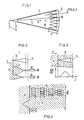
- Fig. 1 shows the essential parts of a device for EMI testing of electronic devices. It comprises a TEM waveguide with an outer conductor 1, an asymmetrical inner conductor 4, a feed wedge 2 and an HF absorber 5.
- HF radio frequency
- the tip of the TEM waveguide widens in a pyramid shape.
- the HF absorber 5 is located at the widened end of the TEM waveguide and has the shape of a spherical cap. It is provided with HF tip absorbers 6 and adapted to the desired wave field that propagates in the TEM waveguide. I.e. it absorbs the field-bound part of the energy of the TEM wave.
- the inner conductor 1 is plate-shaped and is provided with a line termination 7 at the wide end of the TEM waveguide 1.
- This line termination 7 is designed according to the invention so that the conductor-bound part of the energy of the TEM wave is absorbed. No interference can occur due to this line termination and at the same time interference modes that have arisen for other reasons are dampened. In the following the essential points are discussed, which must be considered in order to obtain the desired effects.
- the line termination 7 must be arranged geometrically so that it lies in a surface determined by the inner conductor 4. It thus represents a flat continuation of the inner conductor 4 in the direction of the wave field. (In FIG. 1, an arrow labeled z indicates the direction of the wave field end.) A current flowing in the inner conductor 4 is therefore discharged without kinks. Because the current propagation in the wave direction is not disturbed, there are no undesirable modes.
- the line termination 7 must be designed as an ohmic resistor, which brings about a gradual serial damping of the inner conductor 4. This will be explained with reference to Figures 2 and 3.
- Fig. 2 shows how the inner conductor 4 is completed in the prior art.
- a plan view of the surface of the inner conductor 4 is shown in FIGS. 2 and 3.
- the inner conductor 4 has a tooth-shaped contour in this end region and ends where the HF tip absorbers 6 abut one another.
- the tooth tips are passed through the coherent part of the RF absorber 5 with a wire and terminated behind them with an ohmic resistor R.
- FIG. 3 shows how the line termination 7 according to the invention closes the inner conductor 4.
- the RF absorber 5 and an RF peak absorber 6 are indicated.
- the line termination 7 covers the entire end area T. It also leads through the connected part of the HF absorber 5. It is flat and has a resistance profile dR / dz in the direction of propagation of the wave field, which corresponds to that of the RF absorber 5 additionally compensated for the capacitance on the line termination 7 locally. At every point, the TEM wave "sees" the locally adjusted wave resistance.
- the resistance profile dR / dz increases from a small value at the inner conductor / cable termination transition to a maximum and then drops again to a small value towards the end of the end region.
- the line termination also has a resistance profile which is adapted to the current distribution transverse to the direction of propagation of the TEM wave.
- the resistance profile is transverse to the direction of the wave field, i.e. descending towards the sides from the middle of the line termination. Viewed quantitatively, the resistance profile will therefore have the smallest values at the edges of the line termination.
- the line termination 7 is designed in such a way that a capacitance which is additionally caused on the inner conductor 4 by the RF absorber 5 and the RF peak absorber 6 is locally compensated.
- the line termination 7 according to the invention can preferably be implemented in such a way that a carrier plate, for example a plywood panel, is provided with a resistance layer, for example graphite covering with a suitable location-dependent thickness.
- a metallic, tooth-shaped transition region can be provided on the carrier plate so that the current is conducted from the inner conductor 4 to the resistance covering as free of interference as possible.
- a fiber-reinforced plastic plate is suitable as a carrier plate. Depending on the material, it is covered with a suitable resistance layer or used as resistance itself.
- the invention is not limited to the exemplary embodiments described.
- it is also suitable for open resp. semi-open TEM waveguide, in which the outer conductor is open on one or more sides.
- the invention creates a broadband, reflection-free line termination, which can be used with great advantage wherever high performance has to be destroyed.
Description
Die Erfindung betrifft einen reflexionsfreien Abschluss eines TEM-Wellenleiters, bei welchem eine TEM-Welle durch einen Innenleiter und einen Aussenleiter geführt wird und an einem Ende des TEM-Wellenleiters von einem HF-Absorber zur Absorption der feldgebundenen Energie und einem ohmschen Leitungsabschluss zur Absorption der leitergebundenen Energie der TEM-Welle absorbiert wird.The invention relates to a reflection-free termination of a TEM waveguide, in which a TEM wave is guided through an inner conductor and an outer conductor and at one end of the TEM waveguide by an RF absorber for absorbing the field-bound energy and an ohmic line termination for absorbing the conductor-bound energy of the TEM wave is absorbed.
Aus der Patentanmeldung EP-A1-0246544 ist eine Vorrichtung zur EMI-Prüfung von elektronischen Geräten bekannt. Bei der EMI-Prüfung (EMI = Electrmagnetic Interference) von elektronischen Geräten weist sie gegenüber anderen Messeinrichtungen grosse Vorteile auf. Insbesondere schafft sie eine definierte Feldverteilung über einen weiten Frequenzbereich und kann auch zur breitbandigen Emissionsmessung eingesetzt werden.A device for EMI testing of electronic devices is known from patent application EP-A1-0246544. In the EMI test (EMI = Electromagnetic Interference) of electronic devices, it has great advantages over other measuring devices. In particular, it creates a defined field distribution over a wide frequency range and can also be used for broadband emission measurement.
Allerdings hat es sich gezeigt, dass unerwünschte, örtliche und frequenzabhängige Inhomogenitäten des Wellenfeldes auftreten. Dies hat damit zu tun, dass der Leitungsabschluss nicht hinreichend reflexionsfrei ist.However, it has been shown that undesirable, local and frequency-dependent inhomogeneities of the wave field occur. This has to do with the fact that the line termination is not sufficiently reflection-free.
Ein Leitungsabschluss für TEM-Wellenleiter ist z.B. aus der Offenlegungsschrift DE-3130487A1 bekannt. Insbesondere wird dort der Innenleiter mit Abschlusswiderständen versehen, welche auf Aequipotentiallinien, also quer zur Ausbreitungsrichtung des Wellenfeldes, liegen. Messungen mit solchen Anordnungen haben aber gezeigt, dass diese für Frequenzen oberhalb 100 MHz nicht brauchbar sind.A line termination for TEM waveguides is e.g. known from published patent application DE-3130487A1. In particular, the inner conductor there is provided with terminating resistances which lie on equipotential lines, that is to say transversely to the direction of propagation of the wave field. Measurements with such arrangements have shown, however, that they cannot be used for frequencies above 100 MHz.
Aufgabe der Erfindung ist es, einen reflexionsfreien Abschluss eines TEM-Wellenleiters der eingangs genannten Art zu schaffen.The object of the invention is to provide a reflection-free termination of a TEM waveguide of the type mentioned.
Erfindungsgemäss besteht die Lösung darin, dass bei einem solchen Leitungsabschluss für TEM-Wellenleiter
- a) der Leitungsabschluss in einer durch den Innenleiter bestimmten und in Wellenrichtung liegenden Fläche liegt,
- b) der Leitungsabschluss als ein ohmscher Widerstand ausgebildet ist, welcher eine graduelle, serielle Bedämpfung des Innenleiters bewirkt und
- c) einen durch die HF-Absorber auf dem Leitungsabschluss zusätzlich hervorgerufenen Kapazitätsbelag lokal kompensiert.
- a) the line termination lies in a surface determined by the inner conductor and lying in the direction of the wave,
- b) the line termination is designed as an ohmic resistor, which brings about a gradual, serial damping of the inner conductor, and
- c) locally compensates for an additional capacitance caused by the RF absorbers on the line termination.
Die Absorption der feldgebundenen Energie erfolgt in einer parallel zum ohmschen Abschluss angeordneten Absorberfläche.The field-bound energy is absorbed in an absorber surface arranged parallel to the ohmic termination.
Vorzugsweise weist der Leitungsabschluss gleichzeitig ein an die Stromverteilung quer zur Ausbreitungsrichtung der TEM-Welle angepasstes Widerstandsprofil auf.At the same time, the line termination preferably has a resistance profile which is adapted to the current distribution transverse to the direction of propagation of the TEM wave.
Besonders vorteilhaft ist es, den erfindungsgemässen Leitungsabschluss bei einer Vorrichtung zur EMI-Prüfung elektronischer Geräte einzusetzen, wobei die Vorrichtung einen sich pyramidenfärmig aufweitenden TEM-Wellenleiter umfasst, welcher durch eine feldangepasste, kugelkalottenförmigen HF-Absorber mit HF-Spitzenabsorbern abgeschlossen ist.It is particularly advantageous to use the line termination according to the invention in a device for EMI testing of electronic devices, the device comprising a pyramid-widening TEM waveguide, which is terminated by a field-adapted, spherical cap-shaped HF absorber with HF tip absorbers.
Dadurch wird es möglich, die elektronischen Geräte nicht nur auf Einstrahlung zuverlässig zu testen, sondern auch deren Emission genau zu messen.This makes it possible not only to test the electronic devices reliably for radiation, but also to measure their emissions precisely.
Weitere vorteilhafte Ausführungsformen der Erfindung ergeben sich aus den abhängigen Patentansprüchen.Further advantageous embodiments of the invention result from the dependent patent claims.
Nachfolgend soll die Erfindung anhand von Ausführungsbeispielen und im Zusammenhang mit der Zeichnung näher erläutert werden. Es zeigen:
- Fig. 1
- eine Vorrichtung zur EMI-Prüfung elektronischer Geräte;
- Fig. 2
- einen Leitungsabschluss gemäss dem Stand der Technik;
- Fig. 3
- einen Leitungsabschluss gemäss der Erfindung; und
- Fig. 4
- einen Leitungsabschluss in der Form eines diskreten Widerstandsnetzes.
The invention will be explained in more detail below on the basis of exemplary embodiments and in connection with the drawing. Show it:
- Fig. 1
- a device for EMI testing of electronic devices;
- Fig. 2
- a line qualification according to the state of the art;
- Fig. 3
- a line termination according to the invention; and
- Fig. 4
- a line termination in the form of a discrete resistance network.
Fig. 1 zeigt die wesentlichen Teile einer Vorrichtung zur EMI-Prüfung elektronischer Geräte. Sie umfasst einen TEM-Wellenleiter mit einem Aussenleiter 1, einem asymmetrischen Innenleiter 4, einen Speisekeil 2 und einen HF-Absorber 5. Ein Koaxialkabel 3 führt z.B. eine impuls- oder sinusförmige Hochfrequenz (HF) dem Speisekeil 2 zu, der eine TEM-Welle (TEM = transversal elektromagnetisch) erzeugt und in den TEM-Wellenleiter einkoppelt.Fig. 1 shows the essential parts of a device for EMI testing of electronic devices. It comprises a TEM waveguide with an
Der TEM-Wellenleiter weitet sich von einer Spitze her pyramidenförmig auf. Der HF-Absorber 5 befindet sich am aufgeweiteten Ende des TEM-Wellenleiters und ist kugelkalottenförmig. Er ist mit HF-Spitzenabsorbern 6 versehen und an das gewünschte, sich im TEM-Wellenleiter ausbreitende Wellenfeld angepasst. D.h. er absorbiert den feldgebundenen Teil der Energie der TEM-Welle.The tip of the TEM waveguide widens in a pyramid shape. The
Der TEM-Wellenleiter ist als solcher ausführlich in der Schweizer Patentanmeldung CH-2026/86-9 beschrieben, deren Inhalt hiermit in der vorliegenden Anmeldung eingeschlossen wird.As such, the TEM waveguide is described in detail in Swiss patent application CH-2026 / 86-9, the content of which is hereby included in the present application.
Der Innenleiter 1 ist plattenförmig und ist am breiten Ende des TEM-Wellenleiters 1 mit einem Leitungsabschluss 7 versehen. Dieser Leitungsabschluss 7 ist gemäss der Erfindung so ausgeführt, dass der leitergebundene Teil der Energie der TEM-Welle absorbiert wird. Durch diesen Leitungsabschluss können keine Störungen entstehen und gleichzeitig werden Störmoden, die aus anderen Gründen entstanden sind, bedämpft. Im folgenden werden die wesentlichen Punkte diskutiert, die zu beachten sind, um die gewünschten Effekte zu erhalten.The
Erstens muss der Leitungsabschluss 7 in geometrischer Hinsicht so angeordnet sein, dass er in einer durch den Innenleiter 4 bestimmten Fläche liegt. Er stellt also eine ebene Weiterführung des Innenleiters 4 in Richtung des Wellenfeldes dar. (In Fig. 1 zeigt ein mit z bezeichneter Pfeil die Richtung des Wellenfelddes an.) Ein im Innenleiter 4 fliessender Strom wird also knickfrei abgeführt. Dadurch dass die Stromausbreitung in Wellenrichtung nicht gestört wird, entstehen keine unerwünschten Moden.First, the
Zweitens muss der Leitungsabschluss 7 als ein ohmscher Widerstand ausgebildet sein, welcher eine graduelle serielle Bedämpfung des Innenleiters 4 bewirkt. Dies soll anhand der Figuren 2 und 3 erläutert werden.Second, the
Fig. 2 zeigt, wie der Innenleiter 4 beim Stand der Technik abgeschlossen wird. (in den Figuren 2 und 3 wird eine Draufsicht auf die Fläche des Innenleiters 4 gezeigt.) In einem Endbereich T, welcher durch die Dicke des HF-Absorbers 5 gegeben ist, wird das erzeugte Wellenfeld abgedämpft. Der Innenleiter 4 ist in diesem Endbereich zahnförmig konturiert und endet dort, wo die HF-spitzenabsorber 6 aneinanderstossen. Die Zahnspitzen sind mit einem Draht durch den zusammenhängenden Teil des HF-Absorbers 5 hindurchgeführt und dahinter mit einem ohmschen Widerstand R abgeschlossen.Fig. 2 shows how the
Fig. 3 zeigt wie der erfindungsgemässe Leitungsabschluss 7 den Innenleiter 4 abschliesst. Wie in Fig. 2 sind der HF-Absorber 5 und ein HF-Spitzenabsorber 6 angedeutet. Der Leitungsabschluss 7 deckt den ganzen Endbereich T ab. Er führt also auch durch den zusammenhängenden Teil des HF-Absorbers 5 hindurch. Er ist flächenhaft ausgebildet und besitzt in Ausbreitungsrichtung des Wellenfeldes ein Widerstandsprofil dR/dz, welches den durch den HF-Absorber 5 auf dem Leitungsabschluss 7 zusätzlich hervorgerufenen Kapazitätsbelag lokal kompensiert. An jeder Stelle "sieht" die TEM-Welle also den lokal angepassten Wellenwiderstand.3 shows how the
Im allgemeinen Fall steigt das Widerstandsprofil dR/dz von einem kleinen Wert beim Uebergang Innenleiter/Leitungsabschluss an auf ein Maximum und fällt dann gegen Ende des Endbereichs wieder auf einen kleinen Wert ab.In the general case, the resistance profile dR / dz increases from a small value at the inner conductor / cable termination transition to a maximum and then drops again to a small value towards the end of the end region.
Gemäss einer bevorzugten Ausführungsform der Erfindung weist der Leitungsabschluss gleichzeitig ein an die Stromverteilung quer zur Ausbreitungsrichtung der TEM-Welle angepasstes Widerstandsprofil auf. Auf diese Weise wird vermieden, dass die grossen Stromkomponenten am seitlichen Rand den Innenleiters nicht quer zur Ausbreitungsrichtung der TEM-Welle gestreut werden. Endsprechend ist das Widerstandsprofil quer zur Richtung des Wellenfeldes, d.h. von der Mitte des Leitungsabschlusses gegen die Seiten hin abfallend. Quantitativ betrachtet, wird das Widerstandsprofil also an den Kanten des Leitungsabschlusses die kleinsten Werte haben.According to a preferred embodiment of the invention, the line termination also has a resistance profile which is adapted to the current distribution transverse to the direction of propagation of the TEM wave. In this way it is avoided that the large current components on the side edge of the inner conductor are not scattered transversely to the direction of propagation of the TEM wave. Accordingly, the resistance profile is transverse to the direction of the wave field, i.e. descending towards the sides from the middle of the line termination. Viewed quantitatively, the resistance profile will therefore have the smallest values at the edges of the line termination.
Der Leitungsabschluss 7 ist schliesslich so ausgebildet, dass ein durch dene HF-Absorber 5 und die HF-Spitzenabsorber 6 auf dem Innenleiter 4 zusätzlich hervorgerufener Kapazitätsbelag lokal kompensiert wird.Finally, the
Der erfindungsgemässe Leitungsabschluss 7 lässt sich vorzugsweise so realisieren, dass eine Trägerplatte, z.B. eine Sperrholzplatte, mit einer Widerstandsschicht, z.B. Graphitbelag mit geeigneter ortsabhängiger Dicke, versehen wird. Damit der Strom möglichst störungsfrei vom Innenleiter 4 auf den Widerstandsbelag geführt wird, kann auf der Trägerplatte ein metallischer, zahnförmiger Uebergangsbereich vorgesehen sein.The
Fig. 4 zeigt eine weitere Ausführungsform. Bei dieser ist die ohmsche serielle Bedämpfung des Leitungsabschlusses durch ein Netzwerk von diskreten Widerständen realisiert.4 shows a further embodiment. With this, the ohmic serial attenuation of the line termination is realized by a network of discrete resistors.
Als Trägerplatte eignet sich eine faserverstärkte Kunststoffplatte. Je nach Material wird diese mit einer geeigneten Widerstandsschicht bedeckt oder gleich selbst als Widerstand benutzt.A fiber-reinforced plastic plate is suitable as a carrier plate. Depending on the material, it is covered with a suitable resistance layer or used as resistance itself.
Die Erfindung beschränkt sich jedoch nicht auf die beschriebenen Ausführungsbeispiele. Insbesondere eignet sie sich auch für offene resp. halboffene TEM-Wellenleiter, bei welchen also der Aussenleiter auf ein oder mehreren Seiten offen ist.However, the invention is not limited to the exemplary embodiments described. In particular, it is also suitable for open resp. semi-open TEM waveguide, in which the outer conductor is open on one or more sides.
Im folgenden werden weitere Eigenschaften und Vorteile der Erfindung stichwortartig aufgezählt:
- 1.
- Die Erfindung schafft eine deutlche Qualitätssteigerung in bezug auf die Feldhomogenität im gesamten Testvolumen und Frequenzbereich.
- 2.
- Es ist damit möglich, deutlich grössere Prüfkammern hoher Qualität zu bauen (z.B. für Anlagen und Fahrzeuge).
- 3.
- Die Herstellungskosten des Abschlussbereichs von Breitbandzellen werden gesenkt.
- 4.
- Die Kühlung des flächenhaft verteilten Abschlusswiderstandes ist gegenüber den diskreten Widerständen beim Stand der Technik besser und einfacher. Entsprechend kann die Prüfkammer für höhere Betriebsfeldstärken eingesetzt werden. Ebenso ist dadurch eine grössere Bauhöhe möglich.
- 5.
- Die Hochspannungsfestigkeit wird grösser.
- 6.
- Aufgrund der hohen Feldqualität ist eine präzise Korrelation zu normgerechten Freifeld-Emissionswerten möglich.
- 7.
- Die Erfindung kann auch zum Abschliessen offener Wellenleiteranordnungen eingesetzt werden.
- 8.
- Schliesslich lassen sich gemäss der Erfindung breitbandige, hochleistungs- und hochspannungsfeste Abschlusslasten (sogenannte Dummy-loads) aufbauen.
In the following, further properties and advantages of the invention are listed in key words:
- 1.
- The invention creates a significant increase in quality in terms of field homogeneity in the entire test volume and frequency range.
- 2nd
- It is therefore possible to build significantly larger, high-quality test chambers (e.g. for systems and vehicles).
- 3rd
- The cost of manufacturing the broadband cell termination area will be reduced.
- 4th
- The cooling of the area-wide terminating resistor is better and easier compared to the discrete resistors in the prior art. Accordingly, the test chamber can be used for higher operating field strengths. A larger overall height is also possible.
- 5.
- The high voltage resistance is increasing.
- 6.
- Due to the high field quality, a precise correlation to standard-compliant free field emission values is possible.
- 7.
- The invention can also be used to close open waveguide arrangements.
- 8th.
- Finally, broadband, high-performance and high-voltage-resistant termination loads (so-called dummy loads) can be built up according to the invention.
Abschliessend kann gesagt werden, dass mit der Erfindung ein breitbandiger, reflexionsfreier Leitungsabschluss geschaffen wird, welcher sich überall dort mit grossem Vorteil einsetzen lässt, wo eine hohe Leistung vernichtet werden muss.In conclusion, it can be said that the invention creates a broadband, reflection-free line termination, which can be used with great advantage wherever high performance has to be destroyed.
Claims (10)
Applications Claiming Priority (2)
| Application Number | Priority Date | Filing Date | Title |
|---|---|---|---|
| CH385388 | 1988-10-14 | ||
| CH3853/88 | 1988-10-14 |
Publications (2)
| Publication Number | Publication Date |
|---|---|
| EP0363831A1 EP0363831A1 (en) | 1990-04-18 |
| EP0363831B1 true EP0363831B1 (en) | 1991-12-27 |
Family
ID=4264883
Family Applications (1)
| Application Number | Title | Priority Date | Filing Date |
|---|---|---|---|
| EP89118544A Expired - Lifetime EP0363831B1 (en) | 1988-10-14 | 1989-10-06 | Reflectionless terminal of a tem wave guide |
Country Status (7)
| Country | Link |
|---|---|
| US (1) | US5055806A (en) |
| EP (1) | EP0363831B1 (en) |
| JP (1) | JPH088443B2 (en) |
| CN (1) | CN1012864B (en) |
| CA (1) | CA1323911C (en) |
| DE (1) | DE58900630D1 (en) |
| HK (1) | HK46493A (en) |
Cited By (3)
| Publication number | Priority date | Publication date | Assignee | Title |
|---|---|---|---|---|
| DE4215954A1 (en) * | 1992-02-04 | 1993-08-05 | Rheinhold & Mahla Ag | Electromagnetic wave absorber in closed and screened spaces - has pyramidal frame and filling constituted by plastic foam impregnated with carbon, metal oxide or mixt. |
| DE4418664C1 (en) * | 1994-05-27 | 1995-11-02 | Abb Management Ag | TEM waveguide arrangement |
| DE19501329C1 (en) * | 1995-01-18 | 1996-07-11 | Eupen Kabelwerk | Device for EMI testing of electronic devices |
Families Citing this family (4)
| Publication number | Priority date | Publication date | Assignee | Title |
|---|---|---|---|---|
| DE69101058T2 (en) * | 1991-06-11 | 1994-05-05 | Amplisilence Srl | Device for measuring electromagnetic interference. |
| DE19601348C1 (en) * | 1996-01-17 | 1997-03-13 | Knorr Bremse Electronic Gmbh | TEM waveguide for electromagnetic interference characteristics testing |
| US7042305B2 (en) * | 2002-12-20 | 2006-05-09 | Com Dev Ltd. | Transmission line termination |
| DE102010020022A1 (en) * | 2010-05-10 | 2011-11-10 | Valeo Schalter Und Sensoren Gmbh | Driver assistance device for a vehicle, vehicle and method for operating a radar device |
Family Cites Families (10)
| Publication number | Priority date | Publication date | Assignee | Title |
|---|---|---|---|---|
| US3354412A (en) * | 1965-11-01 | 1967-11-21 | Emc Technology Inc | Stripline termination device having a resistor that is shorter than one quarter wavelength |
| JPS48113336U (en) * | 1972-04-01 | 1973-12-25 | ||
| DE2634812C2 (en) * | 1976-08-03 | 1983-05-05 | Spinner-GmbH Elektrotechnische Fabrik, 8000 München | HF power terminating resistor |
| US4260962A (en) * | 1979-08-06 | 1981-04-07 | Motorola, Inc. | RF Termination for coaxial transmission lines |
| FR2486720A1 (en) * | 1980-07-11 | 1982-01-15 | Thomson Csf | DEVICE FOR TERMINATING A TRANSMISSION LINE, IN HYPERFREQUENCY, AT MINIMUM STATIONARY WAVE RATES |
| DE3130487A1 (en) * | 1981-07-23 | 1983-02-10 | Licentia Patent-Verwaltungs-Gmbh, 6000 Frankfurt | Low-reflection, shielded, metallic simulation chamber for electromagnetic radiation |
| JPS5864102U (en) * | 1981-10-22 | 1983-04-30 | 高木 勝義 | Coaxial type non-reflection terminator |
| IL70865A (en) * | 1984-02-03 | 1987-10-30 | Israel State | Transverse electromagnetic cells adapted for electromagnetic pulse testing |
| DE3503181A1 (en) * | 1985-01-31 | 1986-08-14 | C. Plath Gmbh Nautisch-Elektronische Technik, 2000 Hamburg | Terminating impedance for EMP simulators |
| CH670174A5 (en) * | 1986-05-20 | 1989-05-12 | Bbc Brown Boveri & Cie |
-
1989
- 1989-09-19 CA CA000611864A patent/CA1323911C/en not_active Expired - Fee Related
- 1989-09-20 US US07/409,789 patent/US5055806A/en not_active Expired - Fee Related
- 1989-10-06 DE DE8989118544T patent/DE58900630D1/en not_active Expired - Fee Related
- 1989-10-06 EP EP89118544A patent/EP0363831B1/en not_active Expired - Lifetime
- 1989-10-09 JP JP1263808A patent/JPH088443B2/en not_active Expired - Lifetime
- 1989-10-14 CN CN89108007A patent/CN1012864B/en not_active Expired
-
1993
- 1993-05-13 HK HK464/93A patent/HK46493A/en not_active IP Right Cessation
Cited By (4)
| Publication number | Priority date | Publication date | Assignee | Title |
|---|---|---|---|---|
| DE4215954A1 (en) * | 1992-02-04 | 1993-08-05 | Rheinhold & Mahla Ag | Electromagnetic wave absorber in closed and screened spaces - has pyramidal frame and filling constituted by plastic foam impregnated with carbon, metal oxide or mixt. |
| DE4418664C1 (en) * | 1994-05-27 | 1995-11-02 | Abb Management Ag | TEM waveguide arrangement |
| US5565822A (en) * | 1994-05-27 | 1996-10-15 | Abb Management Ag | TEM waveguide arrangement |
| DE19501329C1 (en) * | 1995-01-18 | 1996-07-11 | Eupen Kabelwerk | Device for EMI testing of electronic devices |
Also Published As
| Publication number | Publication date |
|---|---|
| HK46493A (en) | 1993-05-21 |
| CN1012864B (en) | 1991-06-12 |
| JPH02149102A (en) | 1990-06-07 |
| DE58900630D1 (en) | 1992-02-06 |
| CA1323911C (en) | 1993-11-02 |
| EP0363831A1 (en) | 1990-04-18 |
| CN1041850A (en) | 1990-05-02 |
| US5055806A (en) | 1991-10-08 |
| JPH088443B2 (en) | 1996-01-29 |
Similar Documents
| Publication | Publication Date | Title |
|---|---|---|
| EP0246544B1 (en) | Device for the emi testing of electronic equipments | |
| EP0363831B1 (en) | Reflectionless terminal of a tem wave guide | |
| EP0369273A1 (en) | Method for comparing the quality of HF absorbers | |
| DE4418664C1 (en) | TEM waveguide arrangement | |
| DE2525845C3 (en) | Broadband low-reflection delay line and method for making it | |
| DE3130487A1 (en) | Low-reflection, shielded, metallic simulation chamber for electromagnetic radiation | |
| DE2710506C3 (en) | Broadband directional line | |
| DE2134147A1 (en) | Waveguide | |
| EP0310762B1 (en) | Shielded cell for the generation of electromagnetic waves of the tem type | |
| DE19501329C1 (en) | Device for EMI testing of electronic devices | |
| DE3605430A1 (en) | Device for reducing radar reflection | |
| DE3644205C2 (en) | ||
| DE3842196C2 (en) | Shielded cell for the generation of electromagnetic waves of the transverse electrical type | |
| DD275923A1 (en) | HOLLOWING SPOTLIGHT FOR MICROWAVE HUMIDITY MEASUREMENT | |
| DE2030567A1 (en) | Arrangement for generating damping in a waveguide line | |
| DE1498751A1 (en) | Method and device for testing dielectric material containing foreign material | |
| DE2328451C2 (en) | Arrangement to reduce interference waves in multi-wave waveguides | |
| DE4423544A1 (en) | Device for simulating a strong electromagnetic field in empty space | |
| DE1954260A1 (en) | Microwave test, control or measurement apparatus | |
| DE4305703A1 (en) | Device for testing EMI (electromagnetic interference) | |
| DE2924491A1 (en) | ELECTRONIC UHF DEVICE | |
| WO1998053333A1 (en) | Method and device for generating and receiving electromagnetic fields for test and measurement purposes | |
| DE1033286B (en) | Terminating resistor for waveguide | |
| DE2418780A1 (en) | FLAT CABLE | |
| DE2111291A1 (en) | Arrangement for the absorption of harmonics in waveguides |
Legal Events
| Date | Code | Title | Description |
|---|---|---|---|
| PUAI | Public reference made under article 153(3) epc to a published international application that has entered the european phase |
Free format text: ORIGINAL CODE: 0009012 |
|
| AK | Designated contracting states |
Kind code of ref document: A1 Designated state(s): CH DE FR GB LI SE |
|
| 17P | Request for examination filed |
Effective date: 19901004 |
|
| 17Q | First examination report despatched |
Effective date: 19910123 |
|
| GRAA | (expected) grant |
Free format text: ORIGINAL CODE: 0009210 |
|
| AK | Designated contracting states |
Kind code of ref document: B1 Designated state(s): CH DE FR GB LI SE |
|
| REF | Corresponds to: |
Ref document number: 58900630 Country of ref document: DE Date of ref document: 19920206 |
|
| ET | Fr: translation filed | ||
| GBT | Gb: translation of ep patent filed (gb section 77(6)(a)/1977) | ||
| PLBE | No opposition filed within time limit |
Free format text: ORIGINAL CODE: 0009261 |
|
| STAA | Information on the status of an ep patent application or granted ep patent |
Free format text: STATUS: NO OPPOSITION FILED WITHIN TIME LIMIT |
|
| 26N | No opposition filed | ||
| EAL | Se: european patent in force in sweden |
Ref document number: 89118544.9 |
|
| PGFP | Annual fee paid to national office [announced via postgrant information from national office to epo] |
Ref country code: GB Payment date: 19990913 Year of fee payment: 11 |
|
| PGFP | Annual fee paid to national office [announced via postgrant information from national office to epo] |
Ref country code: CH Payment date: 19990915 Year of fee payment: 11 |
|
| PGFP | Annual fee paid to national office [announced via postgrant information from national office to epo] |
Ref country code: SE Payment date: 19990920 Year of fee payment: 11 Ref country code: FR Payment date: 19990920 Year of fee payment: 11 |
|
| PGFP | Annual fee paid to national office [announced via postgrant information from national office to epo] |
Ref country code: DE Payment date: 19990927 Year of fee payment: 11 |
|
| PG25 | Lapsed in a contracting state [announced via postgrant information from national office to epo] |
Ref country code: GB Free format text: LAPSE BECAUSE OF NON-PAYMENT OF DUE FEES Effective date: 20001006 |
|
| PG25 | Lapsed in a contracting state [announced via postgrant information from national office to epo] |
Ref country code: SE Free format text: THE PATENT HAS BEEN ANNULLED BY A DECISION OF A NATIONAL AUTHORITY Effective date: 20001030 |
|
| PG25 | Lapsed in a contracting state [announced via postgrant information from national office to epo] |
Ref country code: LI Free format text: LAPSE BECAUSE OF NON-PAYMENT OF DUE FEES Effective date: 20001031 Ref country code: CH Free format text: LAPSE BECAUSE OF NON-PAYMENT OF DUE FEES Effective date: 20001031 |
|
| GBPC | Gb: european patent ceased through non-payment of renewal fee |
Effective date: 20001006 |
|
| REG | Reference to a national code |
Ref country code: CH Ref legal event code: PL |
|
| EUG | Se: european patent has lapsed |
Ref document number: 89118544.9 |
|
| PG25 | Lapsed in a contracting state [announced via postgrant information from national office to epo] |
Ref country code: FR Free format text: LAPSE BECAUSE OF NON-PAYMENT OF DUE FEES Effective date: 20010629 |
|
| PG25 | Lapsed in a contracting state [announced via postgrant information from national office to epo] |
Ref country code: DE Free format text: LAPSE BECAUSE OF NON-PAYMENT OF DUE FEES Effective date: 20010703 |
|
| REG | Reference to a national code |
Ref country code: FR Ref legal event code: ST |