EP0360117B1 - Circuit for driving a capacitive load - Google Patents
Circuit for driving a capacitive load Download PDFInfo
- Publication number
- EP0360117B1 EP0360117B1 EP89116766A EP89116766A EP0360117B1 EP 0360117 B1 EP0360117 B1 EP 0360117B1 EP 89116766 A EP89116766 A EP 89116766A EP 89116766 A EP89116766 A EP 89116766A EP 0360117 B1 EP0360117 B1 EP 0360117B1
- Authority
- EP
- European Patent Office
- Prior art keywords
- power source
- switching element
- terminal
- driving circuit
- source terminal
- Prior art date
- Legal status (The legal status is an assumption and is not a legal conclusion. Google has not performed a legal analysis and makes no representation as to the accuracy of the status listed.)
- Expired - Lifetime
Links
Images


Classifications
-
- H—ELECTRICITY
- H03—ELECTRONIC CIRCUITRY
- H03K—PULSE TECHNIQUE
- H03K17/00—Electronic switching or gating, i.e. not by contact-making and –breaking
- H03K17/51—Electronic switching or gating, i.e. not by contact-making and –breaking characterised by the components used
- H03K17/56—Electronic switching or gating, i.e. not by contact-making and –breaking characterised by the components used by the use, as active elements, of semiconductor devices
- H03K17/72—Electronic switching or gating, i.e. not by contact-making and –breaking characterised by the components used by the use, as active elements, of semiconductor devices having more than two PN junctions; having more than three electrodes; having more than one electrode connected to the same conductivity region
- H03K17/735—Switching arrangements with several input- or output-terminals, e.g. multiplexers, distributors
-
- H—ELECTRICITY
- H03—ELECTRONIC CIRCUITRY
- H03K—PULSE TECHNIQUE
- H03K17/00—Electronic switching or gating, i.e. not by contact-making and –breaking
- H03K17/51—Electronic switching or gating, i.e. not by contact-making and –breaking characterised by the components used
- H03K17/56—Electronic switching or gating, i.e. not by contact-making and –breaking characterised by the components used by the use, as active elements, of semiconductor devices
- H03K17/567—Circuits characterised by the use of more than one type of semiconductor device, e.g. BIMOS, composite devices such as IGBT
-
- H—ELECTRICITY
- H03—ELECTRONIC CIRCUITRY
- H03K—PULSE TECHNIQUE
- H03K17/00—Electronic switching or gating, i.e. not by contact-making and –breaking
- H03K17/51—Electronic switching or gating, i.e. not by contact-making and –breaking characterised by the components used
- H03K17/56—Electronic switching or gating, i.e. not by contact-making and –breaking characterised by the components used by the use, as active elements, of semiconductor devices
- H03K17/72—Electronic switching or gating, i.e. not by contact-making and –breaking characterised by the components used by the use, as active elements, of semiconductor devices having more than two PN junctions; having more than three electrodes; having more than one electrode connected to the same conductivity region
- H03K17/73—Electronic switching or gating, i.e. not by contact-making and –breaking characterised by the components used by the use, as active elements, of semiconductor devices having more than two PN junctions; having more than three electrodes; having more than one electrode connected to the same conductivity region for dc voltages or currents
Definitions
- the present invention relates to a driving circuit, and in particular to a driving circuit suitable for a high voltage drive of a capacitive load such as an EL display device.
- a driving circuit according to the preamble of the independent claim 1 is known from document DER ELEKTRONIKER, no. 7, 1983, pages 38-40, H. M. SCHAR "removingsverParkr mit Power FETs".
- a capacitive load such as an EL panel, a piezo-electric element, etc. is driven in general with a high voltage and a high withstand voltage is required for the driving circuit therefor. Further the driving circuit for the capacitive load should be provided in general with a source side switch for charging the load and a sink side switch for discharging the load, which has been once charged.
- the driving circuit for a capacitive matrix load such as an EL panel, etc. it is desired to integrate a number of output channels and at the integration it is an important problem to reduce the electric power consumption in the driving circuit.
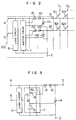
- An example of the driving circuit, in which a thyristor is used, is disclosed in JP-A-60-208119, with an intention of reducing the electric power consumption and increasing the load current driving power. This is shown in Fig. 6.
- a thyristor 8 whose anode and cathode are connected with a power source terminal 201 and an output terminal 3, respectively; a diode 9, whose cathode and anode are connected with the cathode-gate of the thyristor 8 and the cathode thereof respectively; an NPN transistor 11, whose collector and emitter are connected with the anode-gate of the thyristor 8 and a power source terminal 202 through a resistor 12, respectively; and an NPN transistor 10, whose collector and emitter are connected with the cathode-gate of the thyristor 8 and the power source terminal 202, respectively, which constitute an output section.
- the bases of the NPN transistors 10 and 11 are connected with the drains of PMOS transistors 72 and 71, respectively, within a buffer circuit 207 driving the output section described above, responding to signals coming from a logic circuit 206. Further the sources of the PMOS transistors 71 and 72 are connected with a low voltage power source terminal 204.
- the logic circuit 206 controls the buffer circuit 207, responding to the input signal through an input terminal 205 and it can be constructed by a shift register and a latch circuit, etc., in the case where the output section is constructed by integrating a number of channels.
- the drive of a capacitive load connected with the output terminal 3 will be explained below.
- the power source terminal 201 is biased by a positive high voltage V HP ground potential GND.
- the thyristor 8 may be switched-on by turning the NPN transistor 10 to the OFF state.
- the ON drive of the thyristor 8 is effected by drawing-out the gate driving current through the anode-gate of the thyristor 8 by turning-on the PMOS transistor 71 within the buffer circuit 207 to turn-on the NPN transistor 11. This gate driving current is brought about through the power source terminal 201 biased by the high voltage V HP .
- the thyristor 8 is turned to the OFF state by turning-on the NPN transistor 10.
- the NPN transistor 10 is turned-on by turning-on the PMOS transistor 72 within the buffer circuit 207 to supply the base current through the low voltage power source terminal 204. Since in the circuit indicated in Fig. 6 the discharging current from the capacitive load 13 flows through a diode 9 to the NPN transistor 10, the circuit between the cathode-gate and the cathode of the thyristor 8 is reverse-biased and further the cathode-gate of the thyristor 8 is biased towards the GND side by the NPN transistor 10. In this way it is possible to prevent erroneous operations of the thyristor 8.
- the EL panel there are disposed scan side electrodes, to which a high voltage is applied sequentially and selectively, and data side electrodes, to which a relatively low voltage is applied in synchronism therewith, responding to lightening and non-lightening data, which are crossed with each other, an EL layer being formed between the two kinds of electrodes.
- a part put between a scan side electrode and a data side electrode constitutes a pixel, which is equivalent to a capacitive load.
- the light emission starting voltage is as high as about 200 (V) as disclosed in JP-A-60-97394. Since the EL panel has the polarization effect, it can be driven by an AC voltage.
- Fig. 7 shows an example, in which a number of channels of the driving circuits indicated in Fig. 6 are integrated and applied to the drive of the scan side electrodes in an EL panel as described above.
- thyristors 81, 82, ..., NPN transistors 101, 102, ..., 111, 112, ..., resistors 121, 122, ..., etc. corresponding to the thyristor 8 are disposed for every channel, power source terminals 201 and 202 being used in common.
- An output terminal 31, 32, ... for each of the channels corresponds to one line of the scan side electrodes.
- each of C1, C2, etc. corresponds to one line of the data side electrodes and each of the capacitive loads 311, 312, etc. connected between the two kinds of electrodes corresponds to one pixel.
- the capacitive loads 311, 312, etc. are called pixels 311, 312, etc.
- the power source lines therefor i.e. power source terminals 201, 202, 204, etc. in Fig. 7, are floating and control signals are inputted through photo-couplers, etc. Further the potential at the low voltage power source terminal 204 is kept always at about 5 (V) with respect to the potential at the power source terminal 202.
- the power source terminal 201 is biased by the positive high voltage V HP and the power source terminal 202 by 0 (V) and that the data side electrode C1 is biased by 0 (V) and C2 by a voltage V D .
- V HP > V T and V HP - V D ⁇ V T are supposed to be valid.
- the positive high voltage V HP is sent to the scan side electrode 31 by turning-on only the thyristor 81.
- the voltage between the two terminals of the pixel 311 is V HP . Since this voltage exceeds the light emission starting voltage V T , the pixel 311 emits light.
- the pixel 312 since the voltage between the two terminals of the pixel 312 is V HP - V D , and since this voltage does not reach the light emission starting voltage V T , the pixel 312 does not emit light. In this way it is possible to decide emission and non-emission of light by the pixels on the selected scan side electrode (in the case described above scan side electrode 31) by using a relatively low voltage V D applied to the data side electrode.
- the pixel After charging of the pixel and emission (or non-emission) of light have been effected by the positive high voltage V HP , the pixel is discharged to prepare for the succeeding driving timing.
- the discharge of the pixels on the scan side electrode 31 can be effected by turning-on the NPN transistor 101.
- the drive of the scan side electrode 31 is terminated and the succeeding scan side electrode 32 is selected and driven.
- the procedure returns to the selection of the first scan side electrode 31.
- a voltage having a polarity opposite to that used at the last time because of the polarization effect of the EL pixel, it is necessary to apply at this time a voltage having a polarity opposite to that used at the last time.
- the power source terminal 202 is biased by a negative high voltage V HN and the power source terminal 201 by 0 (V) so that only the NPN transistor 101 is turned-on to send the negative high voltage V HN to the scan side electrode 31.
- V HN is supposed to satisfy relationships expressed by
- the thyristor 81 After charging of the pixel and emission (or non-emission) of light by this negative high voltage V HN , the thyristor 81 are turned-on to discharge the pixels on the scan side electrode 31 and the procedure proceeds to the selection of the succeeding scan side electrode 32.
- the ON driving current for the thyristor 8 i.e. the gate driving current
- the gate driving current flows from the power source terminal 201 through the NPN transistor 11 to the power source terminal 202.
- the power source terminal 201 is at a potential higher than that at the power source terminal 202, this gives rise to a problem that electric power consumption due to the gate driving current is great.
- this causes complication of the logic circuit, which in turn gives rise to increase in the chip area.
- the source side or the sink side switching element should have the current limiting function.
- the NPN transistor used on the sink side carries out this function.
- the object of the present invention is to provide a driving circuit capable of solving the problem described above and suitable for driving a capacitive load and more concretely speaking, capable of reducing electric power consumption without complicating the circuit and eliminating the holding current of a thyristor, when it is used.
- the positive high voltage V HP When the positive high voltage V HP is sent to the output terminal, the positive high voltage V HP is applied to the first power source terminal and the second power source terminal is held in the floating state so as to turn-on the source side switching element. Since a potential difference of about 5 (V) is always necessary between the first power source terminal and the second power source terminal, taking the voltage drop in the control section into account, the potential at the second power source terminal is lower than the positive high potential V HP at the first power source terminal by about 5 (V).
- the ON driving current for the source side switching element such as a thyristor can be obtained by making current flow from the first power source terminal to the second power source terminal. In this way it is possible to reduce remarkably the electric power consumption.
- the negative high voltage V HN When the negative high voltage V HN is sent to the output terminal, the negative high voltage V HN is applied to the second power source terminal and the first power source terminal is held in the floating state so as to turn-on the sink side switching element. Since the ON driving current for the sink side switching element can be supplied from the first power source terminal just as by the prior art method, the electric power consumption is small.
- either one of the source side and the sink side switching element can be driven by a low voltage power source. Therefore, in the case where a transistor is used as the switching element, since the driving current, i.e. the base current therefor, can be set so as to be great, it is possible to increase the load current driving power of the switching element. Further, since when the high voltage is applied to either one of the first power source terminal and the second power source terminal, the other is in the floating state, the whole driving circuit is raised or lowered to the potential of the applied high voltage.
- the driving circuit is constructed by integrating a number of channels, even if the output terminals of adjacent channels are short-circuited at the exterior, no short-circuit current of the high voltage power source flows in the driving circuit, but only the loads connected with the short-circuited output terminals are driven simultaneously. For this reason neither the source side nor the sink side switching element should have any particular current limiting function and therefore it is possible to increase easily the current driving power both at the source side and at the sink side by using thyristors for both the switching elements.
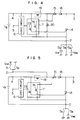
- a thyristor 15 as the source side switching element, in which the anode in connected with a power source terminal 4 and the cathode is connected with the anode of a diode 16, the diode 16, whose cathode is connected with the output terminal 3; and a thyristor 14 as the sink side switching element, in which the anode is connected with the output terminal 3 and the cathode is connected with the other power source terminal 2, these element constituting an output section.
- the cathode-gate of the thyristor 14 is connected with the drain of a PMOS transistor 73 within a buffer circuit 7 and the source of the PMOS transistor 73 is connected with the power source terminal 4.
- the anode-gate of the thyristor 15 is connected with the drain of an NMOS transistor 74 with the buffer circuit 7 and the source of the NMOS transistor is connected with the power source terminal 2. Further there is disposed a logic circuit 6 for controlling the buffer circuit 7 and the output section, responding to the input signal through the input terminal 5. Still further there are disposed a diode 17, in which the anode is connected with the input terminal 5 and the cathode is connected with the power source terminal 4, and another diode 18, in which the anode is connected with the power source terminal 2 and the cathode is connected with the input terminal 5. A capacitive load 13 is connected with the output terminal 3. A low voltage power source V B connected between the power source terminals 2 and 4.
- the low voltage power source V B is a floating power source insulated by means of a transformer, etc. and holds the output terminal 4 at a potential, which is always higher than that at the power source 2 by about 5 V.
- the power source terminal 4 is connected with a positive high voltage power source V HP through an external switching element S1, with the earth potential through a switching element S2; and with a negative high voltage power source V HN through an external switching element S3.
- the power source terminal 2 is connected with a positive high voltage power source V HP through an external switching element S4; with the earth potential through a switching element S5; and with a negative high voltage power source V HN through an external switching element S6.
- the control signal inputted through the input terminal 5 is inputted through an isolator such as a photo-coupler. Now the operation of the driving circuit will be explained below.
- the thyristor 15 is turned-on.
- the thyristor 15 can be turned-on by turning-on the NMOS transistor 74 within the buffer circuit 7 and by drawing-out the gate driving circuit from the anode-gate thereof. Since this gate driving current is supplied by the low voltage power source V B and flows between the power source terminals 4 and 2, the electric power consumption is small.
- the charging current to the capacitive load 13 flows through the path of power source terminal 4 - thyristor 15 - diode 16 - capacitive load 13 - GND.
- the thyristor 14 In the case where the capacitive load 13 charged by the positive high voltage V HP is discharged, in the state where the external switching elements S1, S2, S4, S3, and S6 are turned-off and the external switching element S5 is turned-on, the thyristor 14 is turned-on.
- the thyristor 14 can be turned-on by turning-on the PMOS transistor 73 within the buffer circuit 7 and by supplying the gate driving current to the cathode gate. Since this gate driving current is supplied also by the low voltage power source V B and flows between the power source terminals 4 and 2, the electric power consumption is small.
- the discharging current from the capacitive load 13 flows through the thyristor 14 to the power source terminal 2.
- the external switching elements S1, S2, S3, S5 and S4 are turned-off; the external switching element S6 is turned-on; and the negative high voltage V HN is applied to the power source terminal so that the thyristor 14 is turned-on.
- the charging current flows from the capacitive load 13 to the power source terminal 2 and the capacitive load 13 is charged by the negative high voltage V HN .
- the gate driving current of the thyristor 14 is supplied by the low voltage power source V B similarly to the above description and flows between the power source terminals 4 and 2.
- the external switching elements S1, S3, S4, S5 and S6 are turned-off; the external switching element S2 is turned-on so that the power source terminal 4 is biased at 0 (V); and the thyristor 15 is turned-on.
- the thyristor 15 can be turned-on by turning-on the PMOS transistor 74 so that the gate driving current flows from the power source terminal 4 to the power source terminal 2.
- the discharging current for the capacitive load 13 flows from the power source terminal 4 to the capacitive load 13 through the thyristor 15 and the diode 16.
- the capacitive load 13 it is possible also to charge and discharge the capacitive load 13 only through either one of the power source terminals 2 and 4.
- the load is charged and discharged only through the power source terminal 2
- the current can flow from the power source terminal 2 through the path of diode 18 - diode 17 - thyristor 15 - diode 16 - output terminal 3.
- the thyristor 14 may be turned-on.
- the positive and negative high voltage drive of the capacitive load 13 is possible and in addition it is possible to control both the source side switching element and the sink side switching element by means of a low voltage system of about 5 V, it is possible to reduce remarkably the electric power consumption for driving the high voltage switching elements and to obtain a driving circuit, which is advantageous for the integration.
- the thyristors 14 and 15 are used as the switching elements in order to increase the load driving current power, an identical operation can be carried out, even if the switching elements are constituted by PNP transistors or MOS transistors.
- a base current which is generally greater than the gate driving current for the thyristor, is required and also from the point of view of the load current driving power it is more advantageous to use the thyristors therefor.
- the thyristors are used therefor, although the holding current gives rise to a problem, according to the present embodiment, since an effect of reducing remarkably the electric power consumption due to the gate driving current can be obtained, this problem can be solved by continuing to make the gate current flow during a necessary period of time.
- the thyristors 14 and 15 and the diode 16 are high withstand voltage elements and the thyristor 14 has a high withstand voltage in both the directions, forward and backward.
- the diodes 18 and 17 are disposed generally as input gate protecting elements, which may be utilized therefor.
- the present embodiment is the most suitable for the EL panel scan side driving circuit driven while setting the power source line in the floating state.
- Fig. 2 illustrates an example, in which the driving circuit indicated in Fig. 1 as an embodiment of the present invention is applied to drive of the EL panel scan side electrodes.
- means for giving the power source terminals the potentials are omitted.
- C1, C2, ..., etc. represent data side electrodes and a point, where a scan side electrode and a data side electrode, which are disposed on the different sides of the EL layer, cross each other, corresponds to an EL pixel 311, 312. Further in the used state either one of the power source terminals is in the floating state the power source terminal 4 is held at a potential higher than the potential at the power source terminal 2 by about 5 (V).
- the polarity of the applied voltage is inverted every time to effect the light emission of the pixel.
- the positive high voltage V HP is applied to the power source terminal 4, the power source terminal 2 being in the floating state. If there is a current path from the power source terminal 2 towards the power source terminal 4 such as the diodes 18 and 17 indicated in Fig. 1, the voltage may be applied to either one of the power source terminals 2 and 4.
- the positive high voltage V HP is sent to the scan side electrode 31 by turning-on only the thyristor 151, in the state where the positive high voltage V HP is applied to the power source terminal 4. At this time the pixels 311, 312, ..., etc. on the scan side electrode 31 can be made emit light, depending on the potential state of the data side electrodes C1, C2, ..., etc.
- the power source terminal 4 is set in the floating state; the power source terminal 2 is biased by 0 (V); and the thyristor 141 is turned-on.
- the discharging current flows from the scan side electrode 31 to the power source terminal 2 through the thyristor 141.
- the procedure described above the selection of the scan side electrode 31 is terminated and it proceeds to the selection of the succeeding scan side electrode 32.
- the procedure returns again to the selection of the scan side electrodes 31, at this time, in order to invert the polarity of the voltage applied to the pixels, the negative high voltage V HN should be sent from the output terminal.
- the power source terminal 4 is set in the floating state
- the negative high voltage V HN is applied to the power source terminal 2; and only the thyristor is turned-on.
- the negative high voltage V HN is sent to the side electrode 31 by turning-on the thyristor 141 and the pixels 311, 312, ..., etc. on the scan side electrode 31 can be made emit light, depending on the potential state of the data side electrodes C1, C2, ..., etc.
- the power source terminal 2 is set in the floating state; the power source terminal 4 is biased by 0 (V), and the thyristor 151 is turned-on.
- the discharging current flows from the power source terminal 4 to the scan side electrode 31 through the thyristor 151 and the diode 161 and can discharge the pixels 311, 312, ..., etc. on the scan side electrode 31.
- the present embodiment it is possible to drive the scan electrodes in an EL panel.
- the scanning electrode is composed of generally more than several hundreds of lines and it is necessary for the driving circuit to integrate a number of channels. Since the present invention has the effect of reducing remarkably the electric power consumption, it is very advantageous for the integration. Further recently the EL panel has a tendence to become larger and larger. Since the load current increases therewith, the current driving power of the driving circuit gives rise to a problem. By using thyristors as described in the present embodiment, it is possible to fulfil the requirement stated above without increasing the electric power consumption and to obtain the driving circuit the most suitable for the scan electrode drive of the EL panel.
- Fig. 3 shows another embodiment of the present invention.
- a switching element 76 between the anode and the anode-gate of the thyristor 15 and another switching element 75 between the cathode and the cathode-gate of the thyristor 14.
- the means for giving the power source terminals 2 and 4 the potentials are identical to those described in the embodiment indicated in Fig. 1 and therefore they are omitted. Now the effect obtained by disposing the switching elements 75 and 76 will be explained.
- a resistor is inserted between the cathode-gate and the cathode or the anode-gate and the anode thereof. Further, for the transistor, a resistor is inserted between the base and the emitter. Although this resistor can prevent erroneous operations better with decreasing resistance, since the leak current flowing through this resistor increases correspondingly, which increases the gate driving current or the base current. Further the thyristor has a property of being erroneously lightened by the fact that the rise rate of the applied voltage, i.e. dv/dt, is great.
- a measure for preventing the erroneous operation of the thyristors is taken by bypassing the current flowing through the junction at the application of dv/dt by using the resistor. In this case also, it is possible to prevent better erroneous operations against dv/dt with the decreasing resistance.
- the embodiment indicated in Fig. 3 can prevent erroneous operations of the thyristors 14 and 15 without increasing the gate driving current by disposing the switching elements 75 and 76.
- the switching element 76 is turned-on. In this way, since the anode and the anode-gate of the thyristor 15 are short-circuited, it is possible to prevent erroneous operations of the thyristor 15.
- the cathode-gate and the cathode are short-circuited by turning-on the switching element 75 and it is possible to prevent erroneous operations.
- both the switching elements 75 and 76 can be driven between the power source terminals 4 and 2, it is not necessary to use high withstand voltage elements and therefore the driving circuit can be constructed by using e.g. low voltage MOS transistors, etc. For this reason it is never disadvantageous to form the switching elements in an integrated circuit.
- an effect can be obtained that it is possible to prevent easily erroneous operations of the driving circuit in addition to the effect obtained in the embodiment indicated in Fig. 1 and previously explained.
- the output terminal 3 can be connected with each of the scan electrodes in the EL display device.
- Fig. 4 shows still another embodiment of the present invention.
- the external switching element S4 is turned-on; the positive high voltage V HP is applied to the power source terminal 2; and the thyristor 15 is turned-on.
- the thyristor 15 can be turned-on owing to the fact that the gate driving current flows from the power source terminal 4 to the power source terminal 2 through the switching element 19 and the NMOS transistor 74 by turning-on the switching element 19 and the NMOS transistor 74.
- the power source terminal 4 is held always at a potential higher than that at the power source terminal 2 by about 5 (V) by means of the low voltage power source V B .
- the capacitive load When a capacitive load is connected with the output terminal 3 the capacitive load can be charged up by the positive high voltage V HP from the power source terminal 2 through the diode 20, the thyristor 15 and the diode 16.
- the charging of the load can be effected in the same way.
- the charging current flows through the switching element 19, a current capacity for the switching element 19 is required.
- the external switching element S5 is turned-on; the power source terminal 2 is biased by 0 (V); and the thyristor 14 is turned-on.
- the thyristor 14 is turned-on by turning-on the PMOS transistor 73 to supply the gate driving current from the power source terminal 4 thereto.
- both the thyristors 15 and 14 are in the ON state, which causes the short-circuit between the power source terminals 4 and 2.
- this problem is solved by disposing the switching element 19. That is, when the thyristor 14 side is going to be turned-on, the current path from the power source terminal 4 to the power source terminal 2 through the thyristors 15 and 14 is cut-off by turning-off the switching element 19 and in this way the short-circuit described above can be prevented. Since it is sufficient for the switching element 19 to make a current approximately equal to the gate driving current of the thyristor 15 flow therethrow and it can be composed of a low voltage element, it may be formed by a PMOS transistor, etc. Further, in the case where the circuit indicated in Fig. 4 including a number of channels is formed in an integrated circuit, the thyristor 15, etc. may be disposed by using the cathode side of the diode 20 as the common terminal.
- an effect can be obtained that it is possible to prevent easily erroneous operations of the driving circuit in addition to the effect obtained in the embodiment indicated in Fig. 1.
- Fig. 5 shows a different embodiment of the present invention.
- a power source terminal 21 is disposed between the switching element 19 and the thyristor 15 instead thereof.
- the power source terminal 2 is connected with the earth potential and the negative high voltage power source V HN through the external switching elements S5 and S6, respectively.
- the power source terminal 21 is connected with the positive high voltage power source V HP and the earth potential through external switching elements S1 and S2 respectively.
- the power source terminal 21 is set in the floating state; the power source terminal 2 is biased by 0 V or by the negative high voltage V HN ; and the thyristor 14 side may be turned-on similarly to that described previously.
- the driving circuits indicated in Fig. 4 and 5 can be applied also to the EL display device, as indicated in Fig. 2.
- both the control currents for the source side switching element feeding the load with current and the sink side switching element drawing-out current from the load can be fed and controlled from the low voltage power source, it is possible to obtain an advantageous circuit for driving a capacitive load, capable of reducing remarkably the electric power consumption and being formed in an integrated circuit. Further, when this driving circuit is applied to the drive of an EL display device it is possible to obtain an EL display device having a small electric power consumption and a high current driving power.
Landscapes
- Control Of Indicators Other Than Cathode Ray Tubes (AREA)
- Control Of El Displays (AREA)
Description
- The present invention relates to a driving circuit, and in particular to a driving circuit suitable for a high voltage drive of a capacitive load such as an EL display device.
- A driving circuit according to the preamble of the independent claim 1 is known from document DER ELEKTRONIKER, no. 7, 1983, pages 38-40, H. M. SCHAR "Leistungsverstärker mit Power FETs".
- A capacitive load such as an EL panel, a piezo-electric element, etc. is driven in general with a high voltage and a high withstand voltage is required for the driving circuit therefor. Further the driving circuit for the capacitive load should be provided in general with a source side switch for charging the load and a sink side switch for discharging the load, which has been once charged.
- For the driving circuit for a capacitive matrix load such as an EL panel, etc. it is desired to integrate a number of output channels and at the integration it is an important problem to reduce the electric power consumption in the driving circuit. An example of the driving circuit, in which a thyristor is used, is disclosed in JP-A-60-208119, with an intention of reducing the electric power consumption and increasing the load current driving power. This is shown in Fig. 6.
- In Fig. 6 there are disposed a
thyristor 8, whose anode and cathode are connected with apower source terminal 201 and anoutput terminal 3, respectively; a diode 9, whose cathode and anode are connected with the cathode-gate of thethyristor 8 and the cathode thereof respectively; an NPN transistor 11, whose collector and emitter are connected with the anode-gate of thethyristor 8 and apower source terminal 202 through aresistor 12, respectively; and anNPN transistor 10, whose collector and emitter are connected with the cathode-gate of thethyristor 8 and thepower source terminal 202, respectively, which constitute an output section. The bases of theNPN transistors 10 and 11 are connected with the drains ofPMOS transistors buffer circuit 207 driving the output section described above, responding to signals coming from alogic circuit 206. Further the sources of thePMOS transistors power source terminal 204. Thelogic circuit 206 controls thebuffer circuit 207, responding to the input signal through aninput terminal 205 and it can be constructed by a shift register and a latch circuit, etc., in the case where the output section is constructed by integrating a number of channels. The drive of a capacitive load connected with theoutput terminal 3 will be explained below. - Now it is supposed that the
power source terminal 201 is biased by a positive high voltage VHP ground potential GND. In the case where thecapacitive load 13 is charged by the positive high voltage VHP, thethyristor 8 may be switched-on by turning theNPN transistor 10 to the OFF state. The ON drive of thethyristor 8 is effected by drawing-out the gate driving current through the anode-gate of thethyristor 8 by turning-on thePMOS transistor 71 within thebuffer circuit 207 to turn-on the NPN transistor 11. This gate driving current is brought about through thepower source terminal 201 biased by the high voltage VHP. - Next, in the case where the
capacitive load 13, which has been once charged by the high voltage VHP, is discharged thethyristor 8 is turned to the OFF state by turning-on theNPN transistor 10. TheNPN transistor 10 is turned-on by turning-on thePMOS transistor 72 within thebuffer circuit 207 to supply the base current through the low voltagepower source terminal 204. Since in the circuit indicated in Fig. 6 the discharging current from thecapacitive load 13 flows through a diode 9 to theNPN transistor 10, the circuit between the cathode-gate and the cathode of thethyristor 8 is reverse-biased and further the cathode-gate of thethyristor 8 is biased towards the GND side by theNPN transistor 10. In this way it is possible to prevent erroneous operations of thethyristor 8. - A case where the driving circuit indicated in Fig. 6 is applied to the drive of the EL panel scan side electrodes will be explained below.
- In the EL panel there are disposed scan side electrodes, to which a high voltage is applied sequentially and selectively, and data side electrodes, to which a relatively low voltage is applied in synchronism therewith, responding to lightening and non-lightening data, which are crossed with each other, an EL layer being formed between the two kinds of electrodes. A part put between a scan side electrode and a data side electrode constitutes a pixel, which is equivalent to a capacitive load. The light emission starting voltage is as high as about 200 (V) as disclosed in JP-A-60-97394. Since the EL panel has the polarization effect, it can be driven by an AC voltage. That is, when an EL element is discharged to emit light after having been once charged with a certain voltage polarity, polarization is produced in the direction, where the voltage polarity applied previously is canceled. Therefore, when it is again charged by applying a voltage of same polarity thereto and made emit light, the brightness of the emitted light is reduced. Consequently, in the case where an EL element, which has been once made emit light, should be made again emit light, it is necessary to apply a voltage having a polarity, which is opposite to preceding one, thereto. As examples describing such a method for driving an EL panel, there are known literatures, e.g. "Bidirectional Push-Pull Symmetrical Driving Method For A TF-EL Display (in Japanese)" Sharp Technical Report, Vol. 38, 1987, etc.
- Fig. 7 shows an example, in which a number of channels of the driving circuits indicated in Fig. 6 are integrated and applied to the drive of the scan side electrodes in an EL panel as described above.
- In Fig. 7,
thyristors NPN transistors resistors 121, 122, ..., etc. corresponding to thethyristor 8, theNPN transistor 10, 11 and theresistor 12 indicated in Fig. 6 are disposed for every channel,power source terminals output terminal capacitive loads capacitive loads pixels - Since the circuit for driving the scan side electrodes applies both positive and negative polarity high voltage signals to the data side electrodes, as described also in the example of literature stated above, the power source lines therefor, i.e.
power source terminals power source terminal 204 is kept always at about 5 (V) with respect to the potential at thepower source terminal 202. - At first the case where charging of the pixel and light emission are effected by applying a positive high voltage VHP to the
scan side electrode 31 will be described. - Now it is supposed that the
power source terminal 201 is biased by the positive high voltage VHP and thepower source terminal 202 by 0 (V) and that the data side electrode C1 is biased by 0 (V) and C2 by a voltage VD. Denoting the light emission starting voltage of the EL pixel by VT, relationships expressed by VHP > VT and VHP - VD < VT are supposed to be valid. In this state the positive high voltage VHP is sent to thescan side electrode 31 by turning-on only thethyristor 81. At this time the voltage between the two terminals of thepixel 311 is VHP. Since this voltage exceeds the light emission starting voltage VT, thepixel 311 emits light. On the other hand, since the voltage between the two terminals of thepixel 312 is VHP - VD, and since this voltage does not reach the light emission starting voltage VT, thepixel 312 does not emit light. In this way it is possible to decide emission and non-emission of light by the pixels on the selected scan side electrode (in the case described above scan side electrode 31) by using a relatively low voltage VD applied to the data side electrode. - After charging of the pixel and emission (or non-emission) of light have been effected by the positive high voltage VHP, the pixel is discharged to prepare for the succeeding driving timing. The discharge of the pixels on the
scan side electrode 31 can be effected by turning-on theNPN transistor 101. By the procedure described above the drive of thescan side electrode 31 is terminated and the succeedingscan side electrode 32 is selected and driven. When it is terminated in this way to select and drive all the scan side electrodes, the procedure returns to the selection of the firstscan side electrode 31. However, because of the polarization effect of the EL pixel, it is necessary to apply at this time a voltage having a polarity opposite to that used at the last time. Therefore, at this time, thepower source terminal 202 is biased by a negative high voltage VHN and thepower source terminal 201 by 0 (V) so that only theNPN transistor 101 is turned-on to send the negative high voltage VHN to thescan side electrode 31. Here VHN is supposed to satisfy relationships expressed by |VHN| < VT and |VHN| + VD > VT. - Now, if it is supposed that the data side electrode C1 is biased by 0 (V) and C2 by the voltage VD, since the voltage between the two terminals of the
pixel 311 is |VHN|, the voltage does not reach the light emission starting voltage VT and therefore no light is emitted. On the other hand, for thepixel 312, since the voltage between the two terminals thereof is |VHV| + VD, the voltage applied thereto exceeds the light emission starting voltage VT and light is emitted. - After charging of the pixel and emission (or non-emission) of light by this negative high voltage VHN, the
thyristor 81 are turned-on to discharge the pixels on thescan side electrode 31 and the procedure proceeds to the selection of the succeedingscan side electrode 32. - In the example of literature stated above the method, by which the polarity of the applied voltage is inverted for every scanning electrode, is used. In any case, viewed from a certain scanning electrode, the polarity of the voltage is inverted for every time to select and drive the pixel. For this reason the voltages applied to the
power source terminal - In the prior art circuit the ON driving current for the
thyristor 8, i.e. the gate driving current, flows from thepower source terminal 201 through the NPN transistor 11 to thepower source terminal 202. At this time, since thepower source terminal 201 is at a potential higher than that at thepower source terminal 202, this gives rise to a problem that electric power consumption due to the gate driving current is great. Regarding this point it is possible also to intend to reduce effectively the gate driving current of thethyristor 8 to decrease the electric power consumption by disposing a one-shot circuit within thelogic circuit 206 and by pulse-driving aPMOS transistor 71 and an NPN transistor 11. However this causes complication of the logic circuit, which in turn gives rise to increase in the chip area. Further, in the case of this pulse-driving, after thethyristor 8 has been once turned-on, since there exists no more gate current, when the current flowing through thethyristor 8, i.e. pixel charging current, etc., decreases below the holding current of thethyristor 8, thethyristor 8 is turned-off, which gives rise also to a problem that the charging voltage of the pixel is lowered. In addition, in the case where a number of channels are integrated as indicated in Fig. 7, by the construction of the prior art circuit, since a high potential difference is produced between thepower source terminals power source terminal 202 between different channels. That is, this can take place e.g. in the case where thescan side electrode 31 is selected, to which the high voltage VHP is applied and the otherscan side electrodes 32, ... are at 0V, so that theNPN transistors 102, ..., etc. are turned-on. In order to limit the short-circuit current stated above and to prevent the destruction of the integrated circuit, the source side or the sink side switching element should have the current limiting function. In the examples indicated in Figs. 6 and 7, the NPN transistor used on the sink side carries out this function. - As explained above, in the prior art circuit, in some cases the load driving current power should be limited. This gives rise to a problem, when it is applied to an EL display device, where required current driving power increases with increasing size of the panel.
- The object of the present invention is to provide a driving circuit capable of solving the problem described above and suitable for driving a capacitive load and more concretely speaking, capable of reducing electric power consumption without complicating the circuit and eliminating the holding current of a thyristor, when it is used.
- The above object is achieved by the driving circuit specified in the independent claim 1.
- When the positive high voltage VHP is sent to the output terminal, the positive high voltage VHP is applied to the first power source terminal and the second power source terminal is held in the floating state so as to turn-on the source side switching element. Since a potential difference of about 5 (V) is always necessary between the first power source terminal and the second power source terminal, taking the voltage drop in the control section into account, the potential at the second power source terminal is lower than the positive high potential VHP at the first power source terminal by about 5 (V). The ON driving current for the source side switching element such as a thyristor can be obtained by making current flow from the first power source terminal to the second power source terminal. In this way it is possible to reduce remarkably the electric power consumption. For this reason the problem of the electric power consumption can be solved without using any means for pulse driving, etc. described above. Furthermore it is possible to remove the problem of the holding current, in the case where a thyristor is used, by continuing to make the ON driving current flow during a necessary period.
- When the negative high voltage VHN is sent to the output terminal, the negative high voltage VHN is applied to the second power source terminal and the first power source terminal is held in the floating state so as to turn-on the sink side switching element. Since the ON driving current for the sink side switching element can be supplied from the first power source terminal just as by the prior art method, the electric power consumption is small.
- As described above, either one of the source side and the sink side switching element can be driven by a low voltage power source. Therefore, in the case where a transistor is used as the switching element, since the driving current, i.e. the base current therefor, can be set so as to be great, it is possible to increase the load current driving power of the switching element. Further, since when the high voltage is applied to either one of the first power source terminal and the second power source terminal, the other is in the floating state, the whole driving circuit is raised or lowered to the potential of the applied high voltage. In the case where the driving circuit is constructed by integrating a number of channels, even if the output terminals of adjacent channels are short-circuited at the exterior, no short-circuit current of the high voltage power source flows in the driving circuit, but only the loads connected with the short-circuited output terminals are driven simultaneously. For this reason neither the source side nor the sink side switching element should have any particular current limiting function and therefore it is possible to increase easily the current driving power both at the source side and at the sink side by using thyristors for both the switching elements.
-
- Fig. 1 is a schematic circuit diagram showing an embodiment of the driving circuit according to the present invention;
- Fig. 2 is a schematic circuit diagram of an EL display element using the driving circuit indicated in Fig. 1;
- Fig. 3 is a schematic circuit diagram showing another embodiment of the driving circuit according to the present invention;
- Fig. 4 is a schematic circuit diagram showing still another embodiment of the driving circuit according to the present invention;
- Fig. 5 is a schematic circuit diagram showing a different embodiment of the driving circuit according to the present invention;
- Fig. 6 is a schematic circuit diagram of a prior art driving circuit; and
- Fig. 7 is a schematic circuit diagram of an EL display device using the prior art driving circuit indicated in Fig. 6.
- Hereinbelow the present invention will be explained, referring to the drawings indicating the preferred embodiments.
- In Fig. 1, there are disposed a
thyristor 15 as the source side switching element, in which the anode in connected with apower source terminal 4 and the cathode is connected with the anode of adiode 16, thediode 16, whose cathode is connected with theoutput terminal 3; and athyristor 14 as the sink side switching element, in which the anode is connected with theoutput terminal 3 and the cathode is connected with the otherpower source terminal 2, these element constituting an output section. The cathode-gate of thethyristor 14 is connected with the drain of aPMOS transistor 73 within abuffer circuit 7 and the source of thePMOS transistor 73 is connected with thepower source terminal 4. The anode-gate of thethyristor 15 is connected with the drain of anNMOS transistor 74 with thebuffer circuit 7 and the source of the NMOS transistor is connected with thepower source terminal 2. Further there is disposed alogic circuit 6 for controlling thebuffer circuit 7 and the output section, responding to the input signal through theinput terminal 5. Still further there are disposed adiode 17, in which the anode is connected with theinput terminal 5 and the cathode is connected with thepower source terminal 4, and anotherdiode 18, in which the anode is connected with thepower source terminal 2 and the cathode is connected with theinput terminal 5. Acapacitive load 13 is connected with theoutput terminal 3. A low voltage power source VB connected between thepower source terminals output terminal 4 at a potential, which is always higher than that at thepower source 2 by about 5 V. Thepower source terminal 4 is connected with a positive high voltage power source VHP through an external switching element S₁, with the earth potential through a switching element S₂; and with a negative high voltage power source VHN through an external switching element S₃. On the other hand thepower source terminal 2 is connected with a positive high voltage power source VHP through an external switching element S₄; with the earth potential through a switching element S₅; and with a negative high voltage power source VHN through an external switching element S₆. Furthermore, the control signal inputted through theinput terminal 5 is inputted through an isolator such as a photo-coupler. Now the operation of the driving circuit will be explained below. - At first, in the case where the positive high voltage VHP is sent to the
output terminal 3, in the state where the external switching element S₁ is turned-on and the other external switching elements S₂, S₃, S₄, S₅ and S₆ are turned-off, thethyristor 15 is turned-on. Thethyristor 15 can be turned-on by turning-on theNMOS transistor 74 within thebuffer circuit 7 and by drawing-out the gate driving circuit from the anode-gate thereof. Since this gate driving current is supplied by the low voltage power source VB and flows between thepower source terminals capacitive load 13 flows through the path of power source terminal 4 - thyristor 15 - diode 16 - capacitive load 13 - GND. - In the case where the
capacitive load 13 charged by the positive high voltage VHP is discharged, in the state where the external switching elements S₁, S₂, S₄, S₃, and S₆ are turned-off and the external switching element S₅ is turned-on, thethyristor 14 is turned-on. Thethyristor 14 can be turned-on by turning-on thePMOS transistor 73 within thebuffer circuit 7 and by supplying the gate driving current to the cathode gate. Since this gate driving current is supplied also by the low voltage power source VB and flows between thepower source terminals capacitive load 13 flows through thethyristor 14 to thepower source terminal 2. - Next, in the case where the
capacitive load 13 is charged by the negative high voltage VHN, the external switching elements S₁, S₂, S₃, S₅ and S₄ are turned-off; the external switching element S₆ is turned-on; and the negative high voltage VHN is applied to the power source terminal so that thethyristor 14 is turned-on. When thethyristor 14 is turned-on, the charging current flows from thecapacitive load 13 to thepower source terminal 2 and thecapacitive load 13 is charged by the negative high voltage VHN. At this time the gate driving current of thethyristor 14 is supplied by the low voltage power source VB similarly to the above description and flows between thepower source terminals - In the case where the
capacitive load 13 charged by the negative high voltage VHN is discharged, the external switching elements S₁, S₃, S₄, S₅ and S₆ are turned-off; the external switching element S₂ is turned-on so that thepower source terminal 4 is biased at 0 (V); and thethyristor 15 is turned-on. Just as described in the above, thethyristor 15 can be turned-on by turning-on thePMOS transistor 74 so that the gate driving current flows from thepower source terminal 4 to thepower source terminal 2. By turning-on thethyristor 15 the discharging current for thecapacitive load 13 flows from thepower source terminal 4 to thecapacitive load 13 through thethyristor 15 and thediode 16. - Further, in the present embodiment, it is possible also to charge and discharge the
capacitive load 13 only through either one of thepower source terminals power source terminal 2, when current is supplied to thecapacitive load 13, i.e. at the charging there of by the positive high voltage VHP or at the discharge after having charged it by the negative high voltage, the current can flow from thepower source terminal 2 through the path of diode 18 - diode 17 - thyristor 15 - diode 16 -output terminal 3. On the other hand, in the case where current is drawn out from thecapacitive load 13, just as explained in the above embodiment, thethyristor 14 may be turned-on. - In the case where only the
power source terminal 4 is used, it is possible to charge and discharge thecapacitive load 13 similarly by using the path of thediodes - As described above, in the case where a terminal is used in common for applying the high voltage either one of the groups of the external switching elements S₁, S₂, S₃ and S₄, S₅, S₆ in Fig. 1 can be removed.
- Further, according to the present embodiment, since the positive and negative high voltage drive of the
capacitive load 13 is possible and in addition it is possible to control both the source side switching element and the sink side switching element by means of a low voltage system of about 5 V, it is possible to reduce remarkably the electric power consumption for driving the high voltage switching elements and to obtain a driving circuit, which is advantageous for the integration. In Fig. 1, although thethyristors power source terminals thyristors diode 16 are high withstand voltage elements and thethyristor 14 has a high withstand voltage in both the directions, forward and backward. Further, in the case where thelogic circuit 6 is constructed by CMOS transistors, thediodes - As explained above, since it is possible to drive the capacitive load by using both the positive and the negative high voltage owing to the fact that either one of the
power source terminals - Fig. 2 illustrates an example, in which the driving circuit indicated in Fig. 1 as an embodiment of the present invention is applied to drive of the EL panel scan side electrodes. In this figure, means for giving the power source terminals the potentials are omitted.
- In Fig. 2 a number of the driving circuits indicated in Fig. 1, which is equal to the number of channels, are disposed and the
output terminal EL pixel power source terminal 4 is held at a potential higher than the potential at thepower source terminal 2 by about 5 (V). - Since the EL display panel has the polarization effect as described above, the polarity of the applied voltage is inverted every time to effect the light emission of the pixel. In Fig. 2, in the case where the
scan side electrode 31 is selected and charged by the positive high voltage VHP to make the pixel emit light, the positive high voltage VHP is applied to thepower source terminal 4, thepower source terminal 2 being in the floating state. If there is a current path from thepower source terminal 2 towards thepower source terminal 4 such as thediodes power source terminals scan side electrode 31 by turning-on only thethyristor 151, in the state where the positive high voltage VHP is applied to thepower source terminal 4. At this time thepixels scan side electrode 31 can be made emit light, depending on the potential state of the data side electrodes C₁, C₂, ..., etc. - Next, in the case where the
pixels scan side electrode 31 are discharged, thepower source terminal 4 is set in the floating state; thepower source terminal 2 is biased by 0 (V); and thethyristor 141 is turned-on. The discharging current flows from thescan side electrode 31 to thepower source terminal 2 through thethyristor 141. - By the procedure described above the selection of the
scan side electrode 31 is terminated and it proceeds to the selection of the succeedingscan side electrode 32. After all the scan side electrodes have been successively selected, the procedure returns again to the selection of thescan side electrodes 31, at this time, in order to invert the polarity of the voltage applied to the pixels, the negative high voltage VHN should be sent from the output terminal. In this case thepower source terminal 4 is set in the floating state, the negative high voltage VHN is applied to thepower source terminal 2; and only the thyristor is turned-on. The negative high voltage VHN is sent to theside electrode 31 by turning-on thethyristor 141 and thepixels scan side electrode 31 can be made emit light, depending on the potential state of the data side electrodes C₁, C₂, ..., etc. - Next, in the case where the
pixels power source terminal 2 is set in the floating state; thepower source terminal 4 is biased by 0 (V), and thethyristor 151 is turned-on. The discharging current flows from thepower source terminal 4 to thescan side electrode 31 through thethyristor 151 and thediode 161 and can discharge thepixels scan side electrode 31. - As explained above, according to the present embodiment, it is possible to drive the scan electrodes in an EL panel. The scanning electrode is composed of generally more than several hundreds of lines and it is necessary for the driving circuit to integrate a number of channels. Since the present invention has the effect of reducing remarkably the electric power consumption, it is very advantageous for the integration. Further recently the EL panel has a tendence to become larger and larger. Since the load current increases therewith, the current driving power of the driving circuit gives rise to a problem. By using thyristors as described in the present embodiment, it is possible to fulfil the requirement stated above without increasing the electric power consumption and to obtain the driving circuit the most suitable for the scan electrode drive of the EL panel.
- Fig. 3 shows another embodiment of the present invention.
- In Fig. 3, in addition to the embodiment indicated in Fig. 1, there are disposed a switching element 76 between the anode and the anode-gate of the
thyristor 15 and another switchingelement 75 between the cathode and the cathode-gate of thethyristor 14. Concerning the ON drive of thethyristors PMOS transistor 73 or theNMOS transistor 74 just as described in the embodiment indicated in Fig. 1, while setting theswitching elements 75 and 76 in the OFF state. In the present embodiment the means for giving thepower source terminals elements 75 and 76 will be explained. - In general, in order to secure the reliability concerning the withstand voltage of the thyristor, a resistor is inserted between the cathode-gate and the cathode or the anode-gate and the anode thereof. Further, for the transistor, a resistor is inserted between the base and the emitter. Although this resistor can prevent erroneous operations better with decreasing resistance, since the leak current flowing through this resistor increases correspondingly, which increases the gate driving current or the base current. Further the thyristor has a property of being erroneously lightened by the fact that the rise rate of the applied voltage, i.e. dv/dt, is great. Also in order to prevent this phenomenon, a measure for preventing the erroneous operation of the thyristors is taken by bypassing the current flowing through the junction at the application of dv/dt by using the resistor. In this case also, it is possible to prevent better erroneous operations against dv/dt with the decreasing resistance.
- The embodiment indicated in Fig. 3 can prevent erroneous operations of the
thyristors elements 75 and 76. For example, in the case where the positive high voltage VHP is applied to thepower source terminal 4 and thethyristor 15 is held in the OFF state, the switching element 76 is turned-on. In this way, since the anode and the anode-gate of thethyristor 15 are short-circuited, it is possible to prevent erroneous operations of thethyristor 15. Further, in the case where the negative high voltage VHN is applied to thepower source terminal 2 and thethyristor 14 is held in the OFF state, the cathode-gate and the cathode are short-circuited by turning-on the switchingelement 75 and it is possible to prevent erroneous operations. - Since both the
switching elements 75 and 76 can be driven between thepower source terminals - According to the present embodiment an effect can be obtained that it is possible to prevent easily erroneous operations of the driving circuit in addition to the effect obtained in the embodiment indicated in Fig. 1 and previously explained.
- Also in this embodiment, as indicated in Fig. 2, the
output terminal 3 can be connected with each of the scan electrodes in the EL display device. - Fig. 4 shows still another embodiment of the present invention.
- In Fig. 4, in addition to the embodiment indicated in Fig. 1, there are disposed a switching
element 19 between thepower source terminal 4 and the anode of thethyristor 15 and a diode 20, in which the cathode is connected with the anode of thethyristor 15 and the anode with thepower source terminal 2. It differs from the embodiment indicated in Fig. 1 in that there exist means for giving the power source terminals the potentials only on thepower source terminal 2 side. Hereinbelow the operation thereof will be explained. - At first, in the case where the positive high voltage VHP sent to the
output terminal 3, the external switching element S₄ is turned-on; the positive high voltage VHP is applied to thepower source terminal 2; and thethyristor 15 is turned-on. Thethyristor 15 can be turned-on owing to the fact that the gate driving current flows from thepower source terminal 4 to thepower source terminal 2 through the switchingelement 19 and theNMOS transistor 74 by turning-on the switchingelement 19 and theNMOS transistor 74. Further, just as described previously, thepower source terminal 4 is held always at a potential higher than that at thepower source terminal 2 by about 5 (V) by means of the low voltage power source VB. When a capacitive load is connected with theoutput terminal 3 the capacitive load can be charged up by the positive high voltage VHP from thepower source terminal 2 through the diode 20, thethyristor 15 and thediode 16. In the case where there exists no diode 20, if the positive high voltage VHP is applied to thepower source terminal 4 while holding thepower source terminal 2 in the floating state, or if there exists a path (diode path) from thepower source terminal 2 towards thepower source terminal 4, as indicated in Fig. 1, the charging of the load can be effected in the same way. However, in this case, since the charging current flows through the switchingelement 19, a current capacity for the switchingelement 19 is required. In the case where the load charged by the positive high voltage VHP is discharged, the external switching element S₅ is turned-on; thepower source terminal 2 is biased by 0 (V); and thethyristor 14 is turned-on. Thethyristor 14 is turned-on by turning-on thePMOS transistor 73 to supply the gate driving current from thepower source terminal 4 thereto. At this time, if thethyristor 15 is still in the ON state, both thethyristors power source terminals - In the present embodiment this problem is solved by disposing the switching
element 19. That is, when thethyristor 14 side is going to be turned-on, the current path from thepower source terminal 4 to thepower source terminal 2 through thethyristors element 19 and in this way the short-circuit described above can be prevented. Since it is sufficient for the switchingelement 19 to make a current approximately equal to the gate driving current of thethyristor 15 flow therethrow and it can be composed of a low voltage element, it may be formed by a PMOS transistor, etc. Further, in the case where the circuit indicated in Fig. 4 including a number of channels is formed in an integrated circuit, thethyristor 15, etc. may be disposed by using the cathode side of the diode 20 as the common terminal. - According to the present embodiment an effect can be obtained that it is possible to prevent easily erroneous operations of the driving circuit in addition to the effect obtained in the embodiment indicated in Fig. 1.
- Fig. 5 shows a different embodiment of the present invention.
- In Fig. 5, the diode 20 in Fig. 4 is removed and a
power source terminal 21 is disposed between the switchingelement 19 and thethyristor 15 instead thereof. Thepower source terminal 2 is connected with the earth potential and the negative high voltage power source VHN through the external switching elements S₅ and S₆, respectively. On the other hand thepower source terminal 21 is connected with the positive high voltage power source VHP and the earth potential through external switching elements S₁ and S₂ respectively. - In Fig. 5, in the case where the positive high voltage VHP is sent to the
output terminal 3, the external switching element S₅ and S₆ is turned-off so that thepower source terminal 2 is in the floating state and the external switching element S₁ is turned-on so that the positive high voltage VHP is applied to thepower source terminal 21. In this state thethyristor thyristor 15 is turned-on. Thethyristor 15 is turned-on owing to the fact that the driving current flows from thepower source terminal 4 to thepower source terminal 2 through the switchingelement 19 and theNMOS transistor 74 by turning-on both the switchingelement 19 and theNMOS transistor 74 similarly to that described previously. - In the case where the capacitive load connected with the
output terminal 3 and charged by the positive high voltage VHP is discharged or in the case where the capacitive load is charged by the negative high voltage VHN, thepower source terminal 21 is set in the floating state; thepower source terminal 2 is biased by 0 V or by the negative high voltage VHN; and thethyristor 14 side may be turned-on similarly to that described previously. - According to the present embodiment, an effect similar to that obtained in the embodiment indicated in Fig. 4 described previously can be obtained by disposing the switching
element 19. - The driving circuits indicated in Fig. 4 and 5 can be applied also to the EL display device, as indicated in Fig. 2.
- According to the present invention, since both the control currents for the source side switching element feeding the load with current and the sink side switching element drawing-out current from the load can be fed and controlled from the low voltage power source, it is possible to obtain an advantageous circuit for driving a capacitive load, capable of reducing remarkably the electric power consumption and being formed in an integrated circuit. Further, when this driving circuit is applied to the drive of an EL display device it is possible to obtain an EL display device having a small electric power consumption and a high current driving power.
Claims (17)
- A driving circuit comprising:
a first power source terminal (4);
a second power source terminal (2);
an output terminal (3), with which a capacitive load (13) is connected;
a source side switching element (15) connected between said first power source terminal and said output terminal and supplying current to said load;
a sink side switching element (14) connected between said second power source terminal and said output terminal and drawing-out current from said load; and
a positive high voltage power source (VHP);
a negative high voltage power source (VHN);
a low voltage power source (VB) connected between the first and second power source terminals (4, 2), a voltage of the low voltage power source being lower than that of both of said positive and negative high voltage power sources;
a control section (6) connected between said first power source terminal and said second power source terminal and ON-OFF controlling said source side switching element and said sink side switching element;
characterized in that
said control section is powered by said low voltage power source and that when one of said first and second power source terminal (4; 2) is connected with either one of said positive high voltage power source, said negative high voltage power source or the earth potential, the other (2; 4) is not connected to any of said positive high voltage power source, said negative high voltage power source or the earth potential. - A driving circuit according to claim 1, wherein a diode (16) is connected in series with said source side switching element (15), the conduction direction of said diode being the same as that of said source side switching element.
- A driving circuit according to claim 1,
characterized in that
the source side switching element (15) has
a first principal terminal by which it is connected with said first power source terminal (4),
a second principal terminal by which it is connected with said output terminal (3) through a PN junction element,
a gate terminal by which it is connected with said second power source terminal (2) through a first switching element (74);
the sink side switching element (14) has
a first principal terminal by which it is connected with said output terminal (3),
a second principal terminal by which it is connected with said second power source terminal (2),
a gate terminal by which it is connected with said first power source terminal (4) through a second switching element (73). - A driving circuit according to claim 3,
characterized in that
the gate terminal of the source side switching element (15) is connected with the second power source terminal (2) through said first switching element (74) and with the first principal terminal of the source side switching element through a third switching element (76);
the gate terminal of the sink side switching element (14) is connected with said first power source terminal (4) through said second switching element (73) and with said second power source terminal (2) through a fourth switching element (75). - A driving circuit according to claim 3 or 4,
characterized in that
the first principal terminal of the source side switching element (15) is connected with said first power source terminal (4) through a switching element (19), and
a third power source terminal (21) is disposed between said switching element (19) and said first principal terminal of said source side switching element (15). - A driving circuit according to one of claims 1 to 5,
characterized by
current bypassing means (17, 18; 20) for bypassing current from said first power source terminal (2) towards said first principal terminal of said source side switching element. - A driving circuit according to one of claims 1 to 6, wherein said source side switching element (15) is a thyristor.
- A driving circuit according to one of claims 1 to 6, wherein said sink side switching element (14) is a thyristor.
- A driving circuit according to one of claims 1 to 6, wherein said source side switching element (15) is a PNP transistor.
- A driving circuit according to one of claims 1 to 6, wherein said source side switching element (15) is an MOS transistor.
- A driving circuit according to one of claims 1 to 6, wherein said sink side switching element (14) is an MOS transistor.
- A driving circuit according to one of claims 3 to 6, wherein said first switching element (74) is an MOS transistor.
- A driving circuit according to one of claims 3 to 6, wherein said second switching element (73) is an MOS transistor.
- A driving circuit according to one of claims 4 to 6, wherein said first, second, third and fourth switching elements (74, 73, 76, 75) are MOS transistors.
- A driving circuit according to one of claims 3 to 6, wherein said PN junction element (16) is a diode.
- A driving circuit according to claim 6, wherein said current bypassing means (17, 18) is a diode.
- A driving circuit according to one of the preceding claims, wherein said capacitive load (13) is an EL display panel.
Applications Claiming Priority (2)
| Application Number | Priority Date | Filing Date | Title |
|---|---|---|---|
| JP233433/88 | 1988-09-20 | ||
| JP63233433A JP2664219B2 (en) | 1988-09-20 | 1988-09-20 | Drive circuit |
Publications (3)
| Publication Number | Publication Date |
|---|---|
| EP0360117A2 EP0360117A2 (en) | 1990-03-28 |
| EP0360117A3 EP0360117A3 (en) | 1991-05-08 |
| EP0360117B1 true EP0360117B1 (en) | 1995-08-09 |
Family
ID=16954963
Family Applications (1)
| Application Number | Title | Priority Date | Filing Date |
|---|---|---|---|
| EP89116766A Expired - Lifetime EP0360117B1 (en) | 1988-09-20 | 1989-09-11 | Circuit for driving a capacitive load |
Country Status (5)
| Country | Link |
|---|---|
| US (1) | US5148049A (en) |
| EP (1) | EP0360117B1 (en) |
| JP (1) | JP2664219B2 (en) |
| DE (1) | DE68923748T2 (en) |
| FI (1) | FI98036C (en) |
Families Citing this family (8)
| Publication number | Priority date | Publication date | Assignee | Title |
|---|---|---|---|---|
| JP2953226B2 (en) * | 1992-12-11 | 1999-09-27 | 株式会社デンソー | Reference voltage generation circuit |
| US5852358A (en) * | 1996-12-11 | 1998-12-22 | The Texas A&M University System | Capactive power circuit |
| WO1998026504A1 (en) * | 1996-12-11 | 1998-06-18 | The Texas A & M University System | Capacitive power circuit |
| JP3006534B2 (en) * | 1997-03-31 | 2000-02-07 | 日本電気株式会社 | Semiconductor device |
| JP4359959B2 (en) * | 1999-04-13 | 2009-11-11 | 株式会社デンソー | Capacitive load drive |
| US6376934B1 (en) | 1999-08-18 | 2002-04-23 | Sipex Corporation | Voltage waveform generator |
| FR2803140B1 (en) | 1999-12-24 | 2002-05-31 | St Microelectronics Sa | ANALOGUE VOLTAGE PULSE GENERATOR |
| FR2889345A1 (en) * | 2005-04-04 | 2007-02-02 | Thomson Licensing Sa | MAINTENANCE DEVICE FOR PLASMA PANEL |
Family Cites Families (15)
| Publication number | Priority date | Publication date | Assignee | Title |
|---|---|---|---|---|
| IT1218316B (en) * | 1982-03-17 | 1990-04-12 | Ates Componenti Elettron | COMMUTING CIRCUIT IN COMMUTATION OF INDUCTIVE LOADS, MONOLICALLY INTEGRABLE, INCLUDING A FINAL STAGE IN PUSH-PULL |
| DE3230741A1 (en) * | 1982-08-18 | 1984-02-23 | Siemens AG, 1000 Berlin und 8000 München | SEMICONDUCTOR SWITCH WITH A DISABLE THYRISTOR |
| EP0140349B1 (en) * | 1983-10-28 | 1992-01-02 | Hitachi, Ltd. | Semiconductor switching device |
| US4581542A (en) * | 1983-11-14 | 1986-04-08 | General Electric Company | Driver circuits for emitter switch gate turn-off SCR devices |
| JPS60125015A (en) * | 1983-12-12 | 1985-07-04 | Hitachi Ltd | Inverter circuit |
| JPS60208119A (en) * | 1984-03-30 | 1985-10-19 | Hitachi Ltd | Semiconductor switch |
| US4598213A (en) * | 1984-09-24 | 1986-07-01 | Motorola, Inc. | Bipolar transient driver |
| JP2571766B2 (en) * | 1986-04-30 | 1997-01-16 | 富士通株式会社 | Matrix display panel |
| JPH0795225B2 (en) * | 1986-09-11 | 1995-10-11 | 富士通株式会社 | Matrix display panel drive circuit |
| US4926065A (en) * | 1987-11-17 | 1990-05-15 | Applied Micro Circuits Corporation | Method and apparatus for coupling an ECL output signal using a clamped capacitive bootstrap circuit |
| US4810903A (en) * | 1987-12-14 | 1989-03-07 | Motorola, Inc. | BICMOS driver circuit including submicron on chip voltage source |
| JPH06100889B2 (en) * | 1987-12-21 | 1994-12-12 | 株式会社日立製作所 | Drive circuit |
| US4877980A (en) * | 1988-03-10 | 1989-10-31 | Advanced Micro Devices, Inc. | Time variant drive circuit for high speed bus driver to limit oscillations or ringing on a bus |
| US4874970A (en) * | 1988-05-11 | 1989-10-17 | Applied Micro Circuits Corporation | ECL output with Darlington or common collector-common emitter drive |
| FR2635930B1 (en) * | 1988-08-31 | 1990-11-23 | Sgs Thomson Microelectronics | MONOLITHIC TWO-WAY SWITCH WITH POWER MOS TRANSISTORS |
-
1988
- 1988-09-20 JP JP63233433A patent/JP2664219B2/en not_active Expired - Lifetime
-
1989
- 1989-09-11 DE DE68923748T patent/DE68923748T2/en not_active Expired - Lifetime
- 1989-09-11 US US07/405,230 patent/US5148049A/en not_active Expired - Lifetime
- 1989-09-11 EP EP89116766A patent/EP0360117B1/en not_active Expired - Lifetime
- 1989-09-20 FI FI894456A patent/FI98036C/en active IP Right Grant
Non-Patent Citations (2)
| Title |
|---|
| DER ELEKTRONIKER, no. 7, 1983, pages 38-40, H.M. SCHAR: "Leistungsverstärker mit Power FETs" * |
| E.A. ZUIDERVEEN "Handbuch der digitalen Schaltungen", 1981, FRANZIS, Munich, pages 182, 183 * |
Also Published As
| Publication number | Publication date |
|---|---|
| JPH0282293A (en) | 1990-03-22 |
| US5148049A (en) | 1992-09-15 |
| EP0360117A3 (en) | 1991-05-08 |
| EP0360117A2 (en) | 1990-03-28 |
| DE68923748T2 (en) | 1996-01-18 |
| FI894456A0 (en) | 1989-09-20 |
| FI98036C (en) | 1997-03-25 |
| DE68923748D1 (en) | 1995-09-14 |
| FI894456A (en) | 1990-03-21 |
| JP2664219B2 (en) | 1997-10-15 |
| FI98036B (en) | 1996-12-13 |
Similar Documents
| Publication | Publication Date | Title |
|---|---|---|
| EP0442688A2 (en) | Switching circuit | |
| US7586467B2 (en) | Load drive circuit, integrated circuit, and plasma display | |
| US7605495B2 (en) | Dual supply circuit | |
| EP0562776B1 (en) | Driver circuit for sinking current to two supply voltages | |
| US20090135110A1 (en) | Display apparatus and integrated circuit | |
| EP0360117B1 (en) | Circuit for driving a capacitive load | |
| CN110930936B (en) | Current-driven digital pixel arrangement for micro-light emitting device array | |
| GB2234126A (en) | Circuit protection device | |
| US4471237A (en) | Output protection circuit for preventing a reverse current | |
| US4967100A (en) | Capacitive load driving apparatus | |
| US6894685B2 (en) | Driving method for luminous elements | |
| EP0287525B1 (en) | Transitory current recirculation through a power switching transistor driving an inductive load | |
| US6982688B2 (en) | Driving apparatus for capacitive light emitting element display panel | |
| CN111564144B (en) | Power supply switching control circuit and display device | |
| JP2804259B2 (en) | Drive device for capacitive loads | |
| JP4406969B2 (en) | EL display device | |
| JP4080380B2 (en) | Capacitive load drive | |
| EP0220791A1 (en) | Switching device | |
| JP2539526B2 (en) | Drive circuit | |
| US5616971A (en) | Power switching circuit | |
| JP2703567B2 (en) | Drive circuit and EL display device | |
| JP2703669B2 (en) | Capacitive load drive circuit | |
| JPH1026952A (en) | Capacitive load drive circuit and display device | |
| JP3039092B2 (en) | Short circuit protection circuit | |
| JPH088479B2 (en) | Drive circuit and display device using the drive circuit |
Legal Events
| Date | Code | Title | Description |
|---|---|---|---|
| PUAI | Public reference made under article 153(3) epc to a published international application that has entered the european phase |
Free format text: ORIGINAL CODE: 0009012 |
|
| AK | Designated contracting states |
Kind code of ref document: A2 Designated state(s): DE GB |
|
| 17P | Request for examination filed |
Effective date: 19901122 |
|
| PUAL | Search report despatched |
Free format text: ORIGINAL CODE: 0009013 |
|
| AK | Designated contracting states |
Kind code of ref document: A3 Designated state(s): DE GB |
|
| 17Q | First examination report despatched |
Effective date: 19930809 |
|
| GRAA | (expected) grant |
Free format text: ORIGINAL CODE: 0009210 |
|
| AK | Designated contracting states |
Kind code of ref document: B1 Designated state(s): DE GB |
|
| REF | Corresponds to: |
Ref document number: 68923748 Country of ref document: DE Date of ref document: 19950914 |
|
| PLBE | No opposition filed within time limit |
Free format text: ORIGINAL CODE: 0009261 |
|
| STAA | Information on the status of an ep patent application or granted ep patent |
Free format text: STATUS: NO OPPOSITION FILED WITHIN TIME LIMIT |
|
| 26N | No opposition filed | ||
| REG | Reference to a national code |
Ref country code: GB Ref legal event code: IF02 |
|
| PGFP | Annual fee paid to national office [announced via postgrant information from national office to epo] |
Ref country code: GB Payment date: 20080820 Year of fee payment: 20 |
|
| PGFP | Annual fee paid to national office [announced via postgrant information from national office to epo] |
Ref country code: DE Payment date: 20080908 Year of fee payment: 20 |
|
| REG | Reference to a national code |
Ref country code: GB Ref legal event code: PE20 Expiry date: 20090910 |
|
| PG25 | Lapsed in a contracting state [announced via postgrant information from national office to epo] |
Ref country code: GB Free format text: LAPSE BECAUSE OF EXPIRATION OF PROTECTION Effective date: 20090910 |