EP0358511A2 - Device for detecting positional relationship between two objects - Google Patents
Device for detecting positional relationship between two objects Download PDFInfo
- Publication number
- EP0358511A2 EP0358511A2 EP89309094A EP89309094A EP0358511A2 EP 0358511 A2 EP0358511 A2 EP 0358511A2 EP 89309094 A EP89309094 A EP 89309094A EP 89309094 A EP89309094 A EP 89309094A EP 0358511 A2 EP0358511 A2 EP 0358511A2
- Authority
- EP
- European Patent Office
- Prior art keywords
- wafer
- mask
- spacing
- objects
- light
- Prior art date
- Legal status (The legal status is an assumption and is not a legal conclusion. Google has not performed a legal analysis and makes no representation as to the accuracy of the status listed.)
- Granted
Links
Images


Classifications
-
- G—PHYSICS
- G03—PHOTOGRAPHY; CINEMATOGRAPHY; ANALOGOUS TECHNIQUES USING WAVES OTHER THAN OPTICAL WAVES; ELECTROGRAPHY; HOLOGRAPHY
- G03F—PHOTOMECHANICAL PRODUCTION OF TEXTURED OR PATTERNED SURFACES, e.g. FOR PRINTING, FOR PROCESSING OF SEMICONDUCTOR DEVICES; MATERIALS THEREFOR; ORIGINALS THEREFOR; APPARATUS SPECIALLY ADAPTED THEREFOR
- G03F9/00—Registration or positioning of originals, masks, frames, photographic sheets or textured or patterned surfaces, e.g. automatically
- G03F9/70—Registration or positioning of originals, masks, frames, photographic sheets or textured or patterned surfaces, e.g. automatically for microlithography
- G03F9/7073—Alignment marks and their environment
- G03F9/7076—Mark details, e.g. phase grating mark, temporary mark
-
- G—PHYSICS
- G03—PHOTOGRAPHY; CINEMATOGRAPHY; ANALOGOUS TECHNIQUES USING WAVES OTHER THAN OPTICAL WAVES; ELECTROGRAPHY; HOLOGRAPHY
- G03F—PHOTOMECHANICAL PRODUCTION OF TEXTURED OR PATTERNED SURFACES, e.g. FOR PRINTING, FOR PROCESSING OF SEMICONDUCTOR DEVICES; MATERIALS THEREFOR; ORIGINALS THEREFOR; APPARATUS SPECIALLY ADAPTED THEREFOR
- G03F9/00—Registration or positioning of originals, masks, frames, photographic sheets or textured or patterned surfaces, e.g. automatically
- G03F9/70—Registration or positioning of originals, masks, frames, photographic sheets or textured or patterned surfaces, e.g. automatically for microlithography
- G03F9/7003—Alignment type or strategy, e.g. leveling, global alignment
- G03F9/7023—Aligning or positioning in direction perpendicular to substrate surface
Definitions
- This invention relates generally to an alignment system for correctly positioning an object. More particularly, the invention is concerned with method and apparatus suitably usable, for example, in a semiconductor microcircuit device manufacturing exposure apparatus for lithographically transferring a fine electronic circuit pattern formed on the surface of a first object (original) such as a mask or reticle (hereinafter simply "mask") onto the surface of a second object (workpiece) such as a wafer, for measuring an interval between the mask and the wafer and controlling the same to a desired value, and also for detecting any positional deviation of the mask and the wafer for relatively positioning or aligning the mask and the wafer.
- a semiconductor microcircuit device manufacturing exposure apparatus for lithographically transferring a fine electronic circuit pattern formed on the surface of a first object (original) such as a mask or reticle (hereinafter simply "mask") onto the surface of a second object (workpiece) such as a wafer, for measuring an interval between the mask and the wafer and controlling the same to a desired value, and also
- the relative alignment of a mask and a wafer is one important factor in respect to ensuring improved performance.
- alignment systems employed in recent exposure apparatuses submicron alignment accuracies or more strict accuracies are required in consideration of the demand for higher degree of integration of semiconductor devices.
- alignment patterns are provided on a mask and a wafer and, by utilizing positional information obtainable from these patterns, the mask and wafer are aligned.
- the manner of executing the alignment as an example there is a method wherein the amount of relative deviation of these alignment patterns is detected on the basis of image processing.
- Another method is proposed in U.S. Patent Nos. 4,037,969 and 4,514,858 and Japanese Laid-Open Patent Application, Laid-Open No. Sho 56-157033, wherein so-called zone plates are used as alignment patterns upon which light is projected and wherein the positions of light spots formed on a predetermined plane by lights from the illuminated zone plates are detected.
- an alignment method utilizing a zone plate is relatively insensitive to any defect of an alignment pattern and therefore assures relatively high alignment accuracies, as compared with an alignment method simply using a traditional alignment pattern.
- Figure 1 is a schematic view of a known type alignment system utilizing zone plates.
- a parallel light emanating from a light source 72 passes through a half mirror 74 and is focussed at a point 78 by a condensing lens 76. Thereafter, the light illuminates a mask alignment pattern 68a on a mask 68 and an alignment pattern 60a on a wafer 60 which is placed on a support table 62.
- Each of these alignment patterns 68a and 60a is provided by a reflection type zone plate and functions to form a spot of focused light on a plane perpendicular to an optical axis which contains the point 78. The amount of relative deviation of the positions of these light spots formed on that plane is detected, by directing the focused beams to a detection plane 82 by means of the condensing lens 76 and another lens 80.
- a control circuit 84 actuates a driving circuit 64 to relatively align the mask 68 and the wafer 60.
- Figure 2 illustrates an imaging relationship of lights from the mask alignment pattern 68a and the wafer alignment pattern 60a shown in Figure 1.
- a portion of the light divergently advancing from the point 78 is reflectively diffracted by the mask alignment pattern 68a and forms a spot 78a of focused light at or adjacent to the point 78, the spot representing the mask position.
- Another portion of the light passes through the mask 68 in the form of a zero-th order transmission light and is projected upon the wafer alignment pattern 60a on the wafer 60 surface with its wavefront being unchanged.
- the incident light is reflectively diffracted by the wafer alignment pattern 60a and then passes again through the mask 68 in the form of a zero-th order transmission light, and finally is focused in the neighborhood of the point 78 to form a spot 78b of focused light, representing the wafer position.
- the mask 68 functions merely as a transparent member.
- the position of the spot 78b formed by the wafer alignment pattern 60a in the described manner represents a deviation Os', in the plane perpendicular to the optical axis containing the point 78, of an amount corresponding to the amount of deviation ⁇ of the wafer 60 with respect to the mask 68 in a direction along the mask or wafer surface (in a lateral direction in this case).
- Figure 3 is a schematic view of an interval measuring device of the type as proposed in Japanese Laid-Open Patent Application Sho 61-111402.
- a mask (first object) M and a wafer (second object) W are disposed opposed to each other, and by means of a lens L1, light is focused at a point Ps between the mask M and the wafer W.
- a portion of the light is reflected by the mask M surface and another portion is reflected by the wafer W surface, these lights are projected and focused through a lens L2 at points Pw and P M on the surface of a screen S.
- the interval between the mask M and the wafer W is detected by detecting the spacing between the spots Pw and P M of focused lights upon the screen S surface.
- Figure 4 is a schematic illustration of optical paths in a first embodiment of the present invention
- Figure 5 is a perspective view showing a major part of an apparatus according to this embodiment.
- First object 2 is a mask, for example, and a second object 3 is a wafer, for example, which are disposed opposed to each other with a spacing gm.
- Physical optical elements 6 1 , 6 2 and 6 3 each is provided in a portion of the mask 2, while physical optic elements 7 1 , 7 2 and 7 3 each is provided in a portion of the wafer 3.
- Each of these physical optic elements 6 1 - 6 3 and 7 1 - 7 3 is formed by a Fresnel zone plate or a diffraction grating, for example.
- the mask 2 and the wafer 3 are illustrated as being provided only by these physical optic elements 6 1 - 6 3 and 7 1 - 7 3 .
- Light receiving means 4 and 5 are placed each at a position spaced by Lo from the mask 2. It is seen that Figure 4 shows the state of reflective diffraction light from the wafer 3, being illustrated in Figure 5, and for convenience in explanation, the wafer 3 is illustrated as being a transmission type diffracting element (equivalent to a reflection type one) as viewed from the direction parallel to the mask 2 surface.
- Each of the light receiving means 4 and 5 comprises a line sensor, an area sensor or a position sensing diode (PSD), for example, and is adapted to detect the position of the center of gravity of each inputted light 8 1 , 8 2 or 8 3 as well as the spot configuration thereof.
- the term "center of gravity of light” means such a point that, when in the cross-section of the light a position vector of each point in the section is multiplied by the light intensity of that point and the thus obtained products are integrated over the entire section, the integrated value has a "zero vector".
- the position of such a point at which the light intensity distribution has a peak may be detected and used.
- Central processing unit (CPU) 9 uses the signals from the light receiving means 4 and 5 to detect, for example, the position of the center of gravity of each light 8 1 , 8 2 or 8 3 incident on the light receiving means 4 surface or the shape of the light spots formed thereon, to thereby determine by calculation the spacing gm between the mask 2 and the wafer 3 as well as any lateral deviation in the X-Y plane (i.e. alignment error) of the mask and the wafer, in the manner which will be described later.
- Wafer stage 100 carries thereon the wafer 3 and is adapted to move the same in each of X, Y and Z directions.
- Stage driver 101 is operable in response to an instruction signal based on the calculation made in the CPU 9, to actuate the wafer stage 100 for adjustment of the lateral position of the mask and the wafer as well as for setting the spacing therebetween.
- the situation illustrated in Figure 5 is that, in regard to any positional deviation (alignment error) of the mask 2 and the wafer 3 in a direction contained in the X-Y plane (lateral direction), the deviation in one-dimensional direction (for example, one direction contained in that plane, namely, X direction in this example) is to be detected.
- the mask-and-wafer deviation can not be determined unless three components ⁇ x, Ay and ⁇ (two-dimensional and rotational deviation) are detected.
- optical systems each having such a structure as shown in Figure 5 may be provided at four corners of a rectangular area of a size of 15 mm, for example, in which a semiconductor circuit pattern should be printed.
- This arrangement allows detection of positional deviation in a plane, at four sites. From the data at least at three of them, the three parameters ⁇ x, Ay and ⁇ can be detected. The manner of detection is well-known in the art and, therefore, description thereof will be omitted here.
- the light receiving means 4 and 5 (and the CPU 9, if necessary) are made movable relatively to the mask 2 or the wafer 3.
- FIG. 4 shows details of diffraction of rays in Figure 5, as viewed in a direction (Y direction) perpendicular to the lengthwise direction of the light receiving means 4 or 5, and illustrates the Fresnel zone plate 7 1 , 7 2 and 7 3 of the wafer 3 each being as a transmissive diffraction element which is equivalent to a reflectively diffracting type one.
- the distance between spots 8 1 and 8 2 bears the information concerning any deviation in the plane (alignment error) between the mask and the wafer
- the distance between spots 8 2 and 8 3 bears the information concerning the surface spacing gm.
- the Fresnel zone plates 6 1 - 6 3 on the mask 2 surface have their focal point positions at points Fi, F 2 and F 3 , respectively.
- the zone plate 6 1 is so patterned that it has a diffraction function, which may be equivalent to that of a convex lens, for producing a convergent first order diffraction light
- each of the zone plates 6 2 and 6 3 is so patterned that it has a diffraction function, which may be equivalent to that of a concave lens, for producing a divergent first order diffraction light.
- the Fresnel zone plates 7 1 - 7 3 on the wafer 3 are so patterned that the incident first order diffraction lights are reflectively diffracted by the zone plates 7 1 - 7 3 and are focussed on the detecting means 4 and 5, spaced from the wafer by Lo + gm, to form spots 8 1 , 8 2 and 8 3 of lights.
- the reflectively diffracted light from the wafer 3 goes through the mask 2 to the detecting means 4 or 5, as shown in Figure 5. However, when it passes the mask 2, it simply passes therethrough without being diffracted, as in the form of what can be called a "zero-th order direct transmission light" which is non-diffracted.
- f M1 denotes the distance between the point F 1 and the mask 2 (the focal lengths of the FZP 6 1 as a convex lens)
- f M2 denotes the distance between the point F 2 and the mask 2 (the focal length of the FZP 6 2 as a concave lens)
- f M3 denotes the distance between the point F 3 and the mask 2 (the focal length of the FZP 6 3 as a concave lens).
- f M2 f M3 denotes the distance between the point F 3 and the mask 2 (the focal length of the FZP 6 3 as a concave lens).
- the spots of lights diffracted by the patterns (zone plates) 6 1 - 6 3 of the mask 2 and the patterns (zone plates) 7 1 - 7 3 of the wafer 3 are formed at positions 8 1 , 8 2 and 8 3 , respectively, which are deviated from respective optical axes 10 1 , 10 2 and 10 3 of the corresponding zone plates through distances gi, g 2 and gs.
- the patterns 7 1 - 7 3 of the wafer are designed so as to produce first order diffraction lights by which the points Fi and 8 1 ; the points F 2 and 8 2 ; and the points F3 and 8 3 are in an optically conjugate relationship.
- equations (2) and (3) are substantially the same, and with a deviation between the mask and the wafer in the plane, the spacing (distance) between the spots 8 2 and 8 3 on the sensor surface is substantially unchanged. If, for example, the wafer 3 shifts upwardly by ⁇ in Figure 4, the deviation between optical axes in each pair changes to "A 2 -8" or " ⁇ 3+ ⁇ ". From equations (2) and (3), the changes Ag 2 and Ag 3 in the spacing g 2 and g 3 can be expressed by: Since, f M2 ⁇ f M3 , Ag 2 + ⁇ g3 ⁇ 0 .
- the spacing between the spots 8 2 and 8 3 on the sensor surface is unchanged and, if the spacing between the optical axes 10 2 and 10 3 in the X direction is denoted by 1 2 , then it is l 2 -(g 2 +g 3 ). Therefore, any positional deviation between the mask and the wafer in the X-Y plane (i.e., alignment error) does not result in a change in the spacing between two spots 8 2 and 8 3 on the sensor 4.
- the surface spacing changes by 10 microns, from 71.5 microns to 61.5 microns
- the spacing gm between the mask and the wafer increases by Az
- the spacing g 2 , from the optical axis 10 2 , of the spot 8 2 resulting from the combination of patterns illustrated at part (B), namely, the combination of patterns 6 2 and 7 2 is such as follows:
- g i and g 2 are such as follows:
- the spacing between the spots 8 1 and 8 2 on the sensors 4 and 5 changes.
- the spacing between the spots 8 1 and 8 2 changes by 1000 microns.
- the gap between the mask and the wafer changes by 5 microns, from 71.5 microns to 66.5 microns, the change in the spacing between the spots 8 1 and 8 2 is only 0.16 micron, which is smaller than the resolution 2 micron and can be disregarded without causing inconveniences.
- 2 -(g 2 +g 3 )" between the spots 8 2 and 8 3 at the time of correct mask-to-wafer gap can be determined in accordance with design values. However, they may be detected by trial printing.
- each of the Fresnel zone plate 6 1 - 6 3 and 7 1 - 7 3 shown in Figure 5 has a lens function in respect to both the X direction and the Y direction, any relative displacement between the mask 2 and the wafer 3 in the Y direction causes displacement of the spots 8 1 , 8 2 and 8 3 in the widthwise direction of the line sensor 4 or 5, by an amount corresponding to the amount of relative displacement.
- each of the line sensors 4 and 5 has a sufficient width to ensure that, even with the possible largest deviation of the mask 2 and the wafer 3 in the Y direction, any one of the spots 8 1 , 8 2 and 8 3 does not go out of the sensor.
- each of the Fresnel zone plate 6 1 - 6 3 and 7 1 - 7 3 may comprise a lens having a power only in the lengthwise direction (X direction) of the line sensor 4 or 6, such as, for example, an FZP having a diffraction function like that of a cylindrical lens.
- the spots 8 1 , 8 2 and 8 3 on the sensors 4 and 5 do not shift in the widthwise direction of the sensor.
- any deviation between planes each containing the focal point of the corresponding FZP and a line parallel to the focal line of that FZP and passing through the center of the pattern is taken as ⁇ .
- the combination of FZP patterns illustrated in Figures 4 and 5 is provided on the mask and wafer, and by using part (A) and (B) any lateral positional deviation can be detected while, on the other hand, by using parts (B) and (C), the spacing can be measured.
- the spacing detection has substantially no dependence upon the lateral positional deviation and, on the other hand, the detection of lateral positional deviation has substantially no dependence on the spacing.
- both the alignment detection and the surface spacing detection can be made at high precision. Further, if there occurs wafer tilt (inclination of wafer), since the detection of any positional deviation in the X-Y plane and the detection of the surface spacing are based on the information regarding the spacing of two spots, the spacing of these spots does not change by the wafer tilt. Therefore, the wafer tilt does not result in a detection error.
- the light projecting system for the inputted light 1 or the alignment and gap detecting system, holding the sensors 4 and 5
- a small amount for example, 10 - 20 microns
- there does not occur an error because any positional deviation in the X-Y plane (lateral positional deviation) is detected on the basis of the spacing between the spots 8 1 and 8 2 and the surface spacing between the mask and the wafer is detected on the basis of the spacing between the spots 8 2 and 8 3 .
- Figure 6 illustrates, as an example, the relationship between (i) pattern areas for the patterns of the mask and the wafer, when the mask and the wafer are aligned with each other, and (ii) those lines which contain the optical axes of the patterns and which are in parallel to the Y axis (in this example, the lines 6 1 a, 6 2 a, 6aa, 7 1 a, 7 2 a and 7 3 a).
- the pattern areas of the mask and the wafer are superposed in respect to the Z direction. However, in Figure 6, they are illustrated as being relatively shifted in the Y direction, for convenience in illustration.
- Figure 7 illustrates examples of the manner of formation of signal spot lights 8 1 , 8 2 and 8 3 on the photodetecting means 4 and 5 at the time of the setting of the spacing, in an occasion where there is no lateral positional deviation between the mask and the wafer.
- the spacing between the spots 8 1 and 8 3 and the spacing between spots 8 3 and 8 2 are detected.
- Figure 7 illustrates examples wherein light spots are formed on two line sensors, as a matter of course the arrangement may be such that light spots 8 1 - 8 3 are formed and arrayed on one line sensor.
- Figure 8 shows, as an example, FZP patterns usable in the first embodiment, as well as the relationship of the pattern areas.
- the detecting direction lies in the lateral direction as viewed in the drawing, i.e., X direction.
- Figure 9 illustrates another embodiment.
- the diffraction function of each FZP is such that: an FZP 12 1 on the mask has a diverging function and an FZP 13 1 on the wafer has a converging function.
- an FZP 12 2 on the mask has a converging function and an FZP 13 2 on the wafer has a diverging function.
- an FZP 12 3 on the mask has a converging function and an FZP 13 3 on the wafer has a diverging function.
- part (A) corresponds to a combination of concave and convex lenses
- part (B) corresponds to a combination of convex and concave lenses
- part (C) corresponds to a combination of convex and concave lenses.
- the optical axes 15 1 , 15 2 and 15 3 of the patterns of the Fresnel zone plates on the wafer are set to be shifted relatively to and in parallel to the optical axes 14 1 , 14 2 and 14 3 of the Fresnel zone plates of the mask, by ⁇ 1*,O 2 * and ⁇ 3 * in the illustrated direction.
- Figure 10 shows another embodiment wherein each of Fresnel zone plates 17 1 , 17 2 and 17 3 of a mask has a refracting function in respect to the X direction, in addition to the light converging (or diverging) function.
- the spacing between (i) a spot 21 1 formed on a photodetector 5 by the combination of patterns of the FZP 17 1 and an FZP 18 1 and (ii) a spot 21 2 formed on a photodetector 4 by a combination of patterns of the FZP 17 2 and an FZP 18 2 is used for the detection of any positional deviation (lateral positional deviation) between the mask and the wafer in the X-Y plane.
- the spacing between spots 21 3 and 21 2 formed on the photodetector 4 by the combination of patterns of the FZP 17 3 and an FZP 18 3 is used for the detection of the surface spacing between the mask and the wafer.
- the patterns 17i -17 3 of the mask are designed so that their focal point positions Fi, F 2 and F 3 are made eccentric as illustrated in Figure 10 by ⁇ 1 , ⁇ 2 and ⁇ 3 with respect to the optical axes 19 1 , 19 2 and 19 3 of these patterns.
- the respective focal lengths are denoted by f M1, f M2 and f M3 .
- Reference numerals 20 1 , 20 2 and 20 3 and denote the optical axes of the zone plates 18 1 , 18 2 and 18 3 , respectively.
- the spots of lights from the FZP patterns of the mask and the wafer are formed on the sensors 4 and 5, at distances g 1 , g 2 and g 3 from the optical axes 19 1 , 19 2 and 193 of the mask patterns 17 1 , 17 2 and 17 3 , respectively, in the directions and at positions as illustrated in Figure 10.
- g 1 , g 2 and g 3 from the optical axes 19 1 , 19 2 and 193 of the mask patterns 17 1 , 17 2 and 17 3 , respectively, in the directions and at positions as illustrated in Figure 10.
- three sets of FZP patterns are provided on a mask and a wafer, and one of these sets is used both for the detection of lateral positional deviation and for measurement of the surface spacing.
- Each of the other two sets is used only for the detection of the lateral positional deviation or for the measurement of the surface spacing.
- a set of Fresnel zone plates of the mask and the wafer as illustrated in part (B) are used both for the detection of lateral positional deviation and for detection of the surface spacing.
- the set of mask and wafer Fresnel zone plates shown in part (A) are used for detection of the lateral position, whereas a combination of the mask and wafer Fresnel zone plates shown in part (C) are used for the detection of the surface spacing.
- reference numeral 22 1 , 22 2 and 22 3 denote FZP pattern areas on a mask 2
- reference numerals 23 1 , 23 2 and 23 3 denote FZP pattern areas on a wafer.
- the portions 22 1 and 23 1 are used in a pair, the portions 22 2 and 23 2 are used in another pair, and the portions 22 3 and 23 3 are used in a further pair.
- the mask-to-wafer alignment can be detected on the basis of the spacing between a light spot formed by the combination 22 1 and 23 1 and a light spot formed by the combination 22 2 and 23 2 , on the sensor surface.
- the surface spacing between the mask and the wafer can be detected on the basis of the spacing between a light spot formed by the combination 22 2 and 23 2 and a light spot formed by the combination 22 3 and 23 3 , on the sensor surface.
- Those lines denoted at 22 1 a, 22 2 a, 22 3 a, 23 1 a, 23 2 a and 23aa, parallel to the Y axis and containing the respective principal axes of respective FZP pattern areas, are in such positional relationship as illustrated.
- Figures 12, 13 and 14 show another embodiment, wherein Figure 12 is a perspective view and Figure 13 is a representation of the device as viewed in a direction (Y direction) perpendicular to the lengthwise direction of lines of sensors 4 and 5, the reflectively diffracted light from a wafer being illustrated as an equivalent, transmissibly diffracted light.
- Figure 14 shows the relationship of FZP pattern areas on a mask and a wafer, with the optical axes of the zone plates.
- numerals 24 1 , 24 2 , 24 3 and 25 3 denote Fresnel zone plates provided on the mask
- numerals 25 1 and 25 2 denote Fresnel zone plates provided on the wafer.
- Numerals 24 1 a, 24 2 a, 24 3 a, 25 1 a, 25 2 a and 25 3 a denote those lines parallel to the Y-axis and containing the optical axis of these zone plates, respectively. Any alignment error between the mask and the wafer can be detected by detecting the spacing between a light spot 28 1 , formed by a combination of the patterns 24 1 and 25 1 , and a light spot 28 2 formed by a combination of Fresnel zone plates 24 2 and 25 2 , as illustrated in Figure 13.
- the surface spacing between the mask and the wafer can be detected by detecting the relationship between a light spot 28 2 , formed by a combination of the fresnel zone plates 24 2 and 25 2 , and a light spot 28 3 formed by a combination of the Fresnel zone plates 24 3 and 25 3 (each being provided on the mask).
- An important feature of the embodiment shown in Figures 12 and 13 resides in that, in part (C) of Figure 13, the pattern on the wafer may be omitted. Namely, the light from the FZP 24 3 is simply regularly reflected by the wafer 3 surface and, by means of the FZP patterns 24 3 and 25 3 provided on the mask, the light spot 28 3 to be used for detection of the mask-and-wafer surface spacing is produced.
- the patterns 25 1 and 25 2 on the wafer have their optical axes shifted by ⁇ 1 ' and ⁇ 2 ' from the axes of the patterns on the mask, in the directions as illustrated. Also, the axes of the patterns 24 3 and 25 3 on the mask are mutually deviated by A 3 ', while retaining the parallel relationship.
- the light spots 28 1 , 28 2 and 28 3 formed on the sensors 5 and 4 are at distances gi', g 2 ' and g 3 ' from the axes of the patterns 24 1 , 24 2 and 24 3 on the mask (in the directions as illustrated in Figure 13), the following relations are provided:
- the measurement of the surface spacing between a mask and a wafer can be made without a pattern on the wafer, by using zero-th order reflection light from the wafer.
- a straight grating 25 4 is provided in an area on the wafer 3, having no pattern, so that only a reflecting action is applied by the wafer to the light having been diffracted by the pattern area 24 3 of the mask, for enhancement of the efficiency of impingement of light to the area 25 3 on the mask.
- steppers step-and-repeat type exposure apparatuses
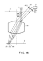
- an optical stepper or an excimer laser stepper that uses an excimer laser. Examples will now be explained with reference to Figures 16 and 17.
- each of the patterns 35 1 - 35 3 on the wafer and the patterns 32 1 -32 3 on the wafer is formed by a diffraction pattern, designed in accordance with the same concept as that of the Figure 4 embodiment disclosed in this Specification.
- the sensors 4 and 5 are disposed adjacent to the reticle 29, it is not always necessary that the reflective diffraction light from the wafer comes back to the reticle side. That is, a mirror or a half mirror may be disposed in the course of this light and, at a position between the wafer and the imaging lens 30, it is directed outwardly of the imaging optical system and then is received by the sensor.
- Figure 17 shows an example wherein the invention is applied to a mirror projection type stepper.
- Reticle 2 and wafer 3 are disposed in an optically conjugate (imaging) relationship, with respect to three groups of mirrors 39, 40 and 41.
- Numerals 43 1 , 43 2 and 43 3 denote FZP patterns provided on the reticle 2
- numerals 44 1 , 44 2 and 44 3 denote FZP patterns provided on the wafer 42.
- These patterns are structured in accordance with the same principle as of the Figure 4 embodiment.
- the principle of detection is the same as of the foregoing embodiment.
- Figure 18 illustrates a modified form of the Figure 4 embodiment.
- the combination of patterns 6 1 and 7 1 ; and 6 2 and 7 2 , illustrated at parts (A) and (B) of Figure 4 is used as it is and the alignment error is detected in the same principle as that of the Figure 4 embodiment.
- the spacing between the mask and the wafer in this example, it is detected on the basis of the position of a spot 8 2 on the sensor 4 surface. This will be explained in more detail.
- a reference position of the spot 8 2 (i.e., the position as assumed when the mask and the wafer have no relative positional deviation and also they are set at a correct spacing) is determined. This can be done on the basis of trial printing, for example. Since values Lo, f M2 and A can be predetermined from design values, the position of the optical axis of the FZP 6 2 , on the surface of the sensor 4, can be determined in accordance with equation (2').
- the alignment error is detected in accordance with the principle described hereinbefore and, subsequently, the detected alignment error is corrected to reduce the same to zero. Then, any deviation of the spot 8 2 at that time from the optical axis position is measured by using the sensor 4 to obtain g 2 and, thereafter, from equation (2') a current spacing gm is detected.
- Figure 19 illustrates another modified form of the Figure 4 embodiment.
- the combination of patterns 6 2 and 7 2 , 6 3 and 7 3 , illustrated at parts (B) and (C) of Figure 4 is used as it is, and the spacing between a mask and a wafer is detected in the same principle as of the Figure 4 embodiment.
- the detection of any alignment error between the mask and the wafer it is made on the basis of the position of a spot 8 2 on the sensor 4 surface. This will be explained in greater detail.
- the reference position as well as the correct spacing gm are detected. Then, in the actual position detecting operation, a current spacing is measured in accordance with the principle described hereinbefore, and subsequently, any error is corrected to establish the correct spacing. Any deviation of the spot 8 2 at that time from its reference position is measured to obtain Ag 2 and, from equation (2") the alignment error 8 is detected.
- Figure 20 is a perspective view of a major part of a ninth embodiment of the present invention.
- Figures 21 and 22 are shematic representations of the major part of the device, as viewed in a direction which is perpendicular to the alignment detecting direction and which is parallel to first and second objects, the optical paths being illustrated in an unfolded state.
- Figures 21 and 22 are different, in respect to the spacing between the first and second objects.
- denoted at 1 is a light supplied from a light source such as, for example, an He-Ne laser or a semiconductor laser.
- Denoted at 2 is a first object which is a mask, for example, and denoted at 3 is a second object which is a wafer, for example.
- the mask 2 and the wafer 3 are disposed opposed to each other with a spacing g AF ( Figures 20 and 21) or a spacing g AA ( Figure 22) maintained therebetween.
- Numerals 106 1 , 106 2 and 106 3 denote first, second and third physical optic elements each being provided in a portion of a mask 2.
- Numerals 107 1 , 107 2 and 107 3 denote first, second and third physical optic elements each being provided in a portion of the water.
- Each of these physical optic elements 106 1 - 106 3 and 107 1 -107 3 is formed, for example, by a diffraction grating or a Fresnel zone plate (which hereinafter will be referred also to simply "FZP").
- Figure 23 shows examples of patterns for the physical optic elements 1061 -1063 and 107 1 - 107 3 to be provided on the mask 2 and the wafer 3.
- first and second light receiving means each comprising a line sensor or a position sensing diode (PSD), for example, and each being adapted to detect, for example, the position of center of gravity of each inputted light 108 1 ,108 2 or 108 3 .
- Signal processing circuit 9 is adapted to process the signals from the light receiving means 4 and 5 to detect, for example, the position of center of gravity of each light 108 1 , 108 2 or 108 3 incident on the light receiving means 4 or 5. Also, the signal processing circuit is adapted to determine, by calculation, any positional error ⁇ and the spacing do, between the mask 2 and the wafer 3.
- Diffraction lights of a predetermined order or orders, diffracted perpendicularly from the mask 2 are reflectively diffracted by the FZP patterns 107 1 ,107 2 and 107 on the wafer 3 surface.
- Those of the diffraction lights of a predetermined order or orders, reflectively diffracted by the FZP patterns 1071 -107 3 on the wafer 3, which pass the mask 2 without being affected thereby (i.e in the form of zero-th order transmission light) are received by the light receiving means 4 and 5.
- the positions of the gravity center of the inputted lights 108i, 1082 and 108 3 , incident on the surfaces of the light receiving means 4 and 5, are detected by these light receiving means 4 and 5.
- the signal processing circuit 9 calculates the amount of positional error between the mask 2 and the wafer 3 as well as the surface spacing between them.
- the present embodiment uses three detection systems, i.e., a detection system A comprising first physical optic elements 106 1 and 107 1 ; a detection system B comprising second physical optic elements 106 2 and 107 2 ; and a detection system C comprising the third physical optic elements 106 3 and 107 3 , provided on the mask 2 and the wafer 3.
- a detection system A comprising first physical optic elements 106 1 and 107 1
- a detection system B comprising second physical optic elements 106 2 and 107 2
- a detection system C comprising the third physical optic elements 106 3 and 107 3 , provided on the mask 2 and the wafer 3.
- the detection system A and the detection system B cooperate to provide a positional deviation detecting system.
- the detection system B is used in common, and the detection systems B and C cooperate to provide a surface spacing detecting system.
- each of the FZP patterns 106 1 , 107 2 and 107 3 has a converging, positive power, while each of the FZP patterns 106 2 , 106 3 and 107 1 has a diverging, negative power.
- the Fresnel zone plate is not limited to one having a refracting or diverging function only in respect to the alignment direction. Namely, in this embodiment, such a Fresnel zone plate as having two-dimensional refracting or diverging function is usable.
- the mask 2 and the wafer 3 are disposed close to each other (the surface spacing is 5 -100 microns, for example), as that the arrangement is suitably incorporated into what can be called an "X-ray stepper" wherein the exposure is made by using X-rays.
- an exposure area per one exposure using X-rays is of a size 10 to several tens millimeters square, and while intermittently shifting the wafer 3 position, exposures of twenty (20) to several tens shots are made.
- the spacing between a mask and a wafer at the time of relative movement of them, for each shot differs from the spacing between the mask and the wafer as measured just before the initiation of the exposure operation through a positional deviation detecting system (auto alignment system).
- the surface spacing illustrated in Figure 22 is one as assumed at the time of autoalignment, and it is of an order of 5 -100 microns as described hereinbefore. As compared therewith, the surface spacing illustrated in Figure 21 is one as assumed at the time of wafer movement, and it is large, of a value of 50 - 200 microns.
- the surface spacing at the time of wafer movement is set to be large. This is made so as to prevent contact of the wafer with the mask surface during movement of the former along the X-Y plane, due to any surface height irregularity to tilt (inclination) of the wafer.
- the spacing 9AF in Figure 21 is one for which the mask and the wafer are set for execution of the wafer movement (shot area movement) and, in this state, the actual spacing between the mask and the wafer is detected. This is called "autofocusing".
- the spacing g AA shown in Figure 22 is one for which the mask and the wafer are set for execution of detection of any positional deviation therebetween (autoalignment), the mask and the wafer being set to this spacing on the basis of the measurement of the surface spacing as the mask and the wafer are placed at the spacing g AF in Figure 21.
- the mask 2 and the wafer 3 have relative positional deviation of an amount 8 in respect to a vertical direction as viewed in the sheet of the drawing.
- the light spots 108 1 , 108 2 an 108 3 formed on the sensors 4 and 5 are at the positions of distances yi, y 2 and y 3 , respectively, from the optical axes (pattern axes) 111 1 , 111 2 and 111 3 of the FZP patterns 106 1 ,106 2 and 106 3 on the mask 2, respectively.
- Numerals 112 1 , 112 2 and 112 3 denote the axes of the FZP patterns 107 1 , 107 2 and 107 3 , respectively, on the wafer.
- the powers of the Fresnel zone plates 106 1 , 107 1 , 106 2 and 107 2 of the mask and the wafer are so set that, when the mask and the wafer is at the spacing g AA , spots 108 1 and 108 2 of smallest diameter are formed on the sensor 5. Also, the arrangement is such that, when the mask and the wafer is at the spacing g AF , a spot 108 3 of smallest diameter is formed on the sensor 104.
- a diffraction spot 108 1 ' provided by a detection system A comprising the combination of the FZP patterns 106 1 and 107 1 , has a smallest diameter
- a diffraction spot 108 2 ' provided by a detection system B comprising the combination of the FZP patterns 106 2 and 107 2
- a diffraction spot 108 3 ' provided by a detection system C comprising the combination of the FZP patterns 106 3 and 107 3
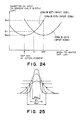
- each FZP on the mask or wafer has a pattern such as shown in Figure 23, for example, and each pattern on the wafer is provided in a scribe line. Due to the diffraction effect of each of the Fresnel zone plates 106 1 and 107 1 ; 106 2 and 107 2 ; and 106 3 and 107 3 , a change in the gap between the mask 102 and the wafer 103 causes a change in the diameter of each spot of the sensor 4 or 5 surface, since the imaging relationship is determined by the focal lengths of the Fresnel zone plates on the mask and the wafer. The manner of such change is illustrated in Figure 24, by way of example. Figure 24 shows this change, in terms of a half width of each light spot on the sensor 4 or 5.
- Figure 25 illustrates the relationship between a half width ⁇ AA and a change in the diameter of a diffraction spot provided by the detection system A, for example, comprising the combination of the FZP patterns 106 1 and 107 1 . Setting is made so that, when the spacing becomes equal to that for the autoalignment (see Figure 22, part (A)), the spot diameter becomes smallest. For a larger spacing g b or larger spacing g AF , the half width 0 1 or Q AF becomes gradually larger.
- the half width on the sensor 5 of a spot of light diffracted by the detection system B, comprising a combination of the FZP patterns 106 2 and 107 2 , as well as the half width on the sensor 4 of a spot of light diffracted by the detection system C, comprising a combination of the FZP patterns 106 3 and 107 3 , are set such as shown in Figure 24.
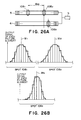
- the state of spots on the sensors 5 and 4 when the mask and the wafer are at the spacing g AF , as in Figure 21, is illustrated in Figure 26A.
- the spacing between the spots 108 1 and 108 2 in the alignment detecting direction e.g. the distance between the positions of gravity centers
- the size of each of the spots 108 2 and 108 3 e.g., a width that corresponds to a half of a peak value
- the diffraction by the combination of FZP patterns 106 2 and 107 2 is set so that the spot on the sensor surface becomes smallest when the spacing is equal to g AA .
- the displacement of the spot on the sensor is of an amount one-hundred (100) times larger than the positional deviation between the mask and the wafer.
- the diffraction by the detecting system C comprising the combination of FZP patterns 106 3 and 107 3 , is set so that the spot on the sensor surface becomes smallest when the spacing is equal to g AF .
- f M1 " 211.94 microns.
- f M2 " 155.62 microns.
- f M3 " 114.53 microns.
- the position deviation (alignment error) between the mask and the wafer is detectable.
- a deviation between the mask and the wafer of an amount 2 microns causes a change in the spacing between the light spots 108 1 ' and 108 2 ' on the sensor surface by 400 microns.
- the spacing between the mask and the wafer is measured, not by measuring the spacing between the spots 108 2 and 108 3 on the sensor surface, but by measuring the size of each of the spots 108 2 and 108 3 , in the manner described with reference to Figure 24.
- a spot has an intensity distribution, like an Airy pattern called in the field of lenses, in this example, it is considered that the spot has such as distribution of intensity like that.
- a functional form of polynominal is applied to some bits, around the maximum output bit, of a line sensor, a maximum value in a spatially continuous output distribution on the sensor surface is obtainable from actually measured values of the output of these bits.
- the maximum value is expressed by lmax, detection may be made to obtain a spatial value on the sensor that correspond to "lmax/2", from interruptedly changing outputs.
- the half width of the light spot 108 2 can be determined with a precision of an order of 1/10- 1/30 of the sensor bit size.
- the spot diameter is about 200 - 800 microns.
- the sensor bit size is about500 microns x 15 microns (pitch)
- the precision of detection of the half width of the spot can be 1 microns. Accordingly, by utilizing the characteristics that the spot half width changes such as shown in Figure 24, it is possible to detect the spacing between the mask and the wafer on the basis of detection of the half width of the spot 108 2 and the half width of the spot 108 3 . While the relationship between the mask-and-wafer spacing and these half widths can be predetermined in accordance with design values, such relationship may be detected by experiments.
- the detection system B which comprises a combination of Fresnel zone plates 106 2 and 107 2 , is used both for the autoalignment and for the autofocusing. This allows that, with a relatively small pattern area surface such as shown in Figure 23, the two functions of autoalignment and autofocusing are provided.
- the spots 108 1 ' and 108 2 ' provide the information related to the positional deviation between the mask and the wafer, even if, as an example, the wafer is inclined or the relative positional relationship of the alignment detecting system (sensors 4 and 5 and detection processing portion 9 in Figure 20) with the mask and the wafer changes slightly, the spots 108 1 ' and 108 2 ' on the sensor 5 changes by the same amount and the spacing itself between these spots is not affected by the wafer inclination or an error in the relative position of the detecting system with respect to the mask and the wafer. Therefore, stable detection is attained.
- the structure may be such that an aerial image of the light spot formed at the sensor 4 and 5 position is relayed by a lens system and the light therefrom may be projected to a line sensor or an area sensor.
- the alignment (autoalignment) of the mask and the wafer is executed by using those Fresnel zone plates on the mask and the wafer having lens functions like a convex-concave system and a concave-convex system, while the detection of the surface spacing between the mask and the wafer (autofocusing) is executed by using a concave-convex system and a concave-convex system.
- the power arrangement may be set as desired.
- the autofocusing may be made by using a concave-convex system and a convex-concave system.
- any combination is usable provided that the focal lengths of the mask patterns and wafer patterns are adjusted and set so that the size of each of the spots, corresponding to the spots 108 2 and 108 3 , changes with the spacing between the mask and the wafer.
- a two-dimensional area sensor may be used for the sensors 4 and 5 of the present embodiment. Further, the sensor arrangement may be made so that three light spots are projected to a single line sensor.
- Figures 27 and 28 are schematic views, respectively, of a major part of a tenth embodiment of the present invention. Like Figures 21 and 22, Figures 27 and 28 show the optical paths, in an unfolded view, as the spacing between a first object (mask) 2 and a second object (wafer) 3 are changed, and these Figures show the device as viewed in a direction perpendicular to the alignment detecting direction.
- the autoalignment is executed by using a concave-convex system (detection system A) and a convex-concave system (detection system B), and is made by detecting the change in the spacing, on the sensor surface, between two spots obtained from these two detection systems.
- the autofocusing is executed by using the convex-concave system (detection system B) and a convex-concave system (detection system C), and is made by detecting the size of each spot obtained from these two detection systems.
- numerals 118 1 , 118 2 , 118 3 and 118 4 each denotes an FZP.
- the example shown in Figure 29 is of proximity type wherein a mask and a wafer are disposed close to each other.
- numerals 119 1 , 119 2 , 119 3 and 119 4 each denotes a detection system for executing the autoalignment or the autofocusing.
- Numerals 121 1 , 121 2 , 121 3 and 121 4 s each denotes a light projected on a pattern.
- numerals 122 1 , 122 2 , 122 3 and 122 4 each denotes a signal light which is obtainable as a result of diffraction by a combination of corresponding Fresnel zone plates of the mask and the wafer.
- the signal light comprises plural spots.
- the detection system 119 1 has an ability of detecting one-dimensional lateral deviation in the X direction.
- the detection system 119 2 , the detection system 119 3 and the detection system 119 4 have respective abilities for detecting positional deviations in the Y direction, X direction and Y direction, respectively.
- the spacing between the mask and the wafer is detected at the four points near the Fresnel zone plates 118 1 , 118 2 , 118 3 and 118 4 .
- Figure 30 is a perspective view of a major part of an eleventh embodiment of the present invention.
- one of sets of diffraction patterns, from a mask and a wafer, each producing two spots for detection of the spacing between the mask and the wafer uses zero-th order regular reflection by the wafer. That is, the present embodiment is an example wherein the wafer surface may have no pattern.
- numerals 123 1 , 123 2 and 123 3 each denotes an FZP on the mask.
- Figure 31 illustrates detailes of diffraction, as viewed in a direction perpendicular to the alignment detecting direction ( Figure 30) and in parallel to the mask and the wafer, wherein the reflective diffraction by the wafer being illustrated as an equivalent, transmissive diffraction wave.
- a pattern of a FZP 124 3 is provided on the mask, and by detecting the spacing between (i) a spot obtainable by diffraction at a detection system A, comprising a combination of FZP patterns 123 1 and 124 1 , and (ii) a spot 127 2 obtainable by diffraction at a detection system B, comprising a combination of FZP patterns 123 2 and 124 2 , the mask-to-wafer deviation (alignment error) is detected.
- the surface spacing (gap) between the mask and the wafer is detected by detecting the size of a spot 127 2 , on a sensor 5 surface, obtainable by diffraction at the detection system B comprising the combination at FZP patterns 123 2 and 124 2 , and the size of the spot 127 3 , on a sensor 4 surface, obtainable by diffraction at a detection system C, comprising a combination of FZP patterns 123 3 and 124 3 .
- optical function of the remaining portion is the same as that of the ninth embodiment.
- the surface spacing between the Fresnel zone plates 123 3 and 124 3 is equal to 2 x g AF , and the focal lengths and the imaging relationship of the patterns of these zone plates are set in consideration of it.
- the spacing between (i) a spot 127 1 produced by the combination of FZP patterns 123 1 and 124 1 (combined power of a concave-convex system) and (ii) a spot 127 2 produced by a combination of FZP patterns 123 2 and 124 2 (combined power of a convex- concave system) is calculated. Then, from the detected spacing, the positional deviation (alignment error) between the mask and the wafer is detected.
- Each of the FZP patterns 123 1 - 123 3 and 124 1 - 124 3 has a lens function only in respect to the alignment detecting direction. However, it may have a lens function in respect to two-dimensional directions and, additionally, an area sensor may be used in place of the line sensors to detect the motion of each light spot.
- the setting is such that each of a spot produced by a combination of FZP patterns 123 1 and 124 1 and a spot produced by FZP patterns 123 2 and 124 2 , all being used for the autoalignment, becomes smallest when the spacing g AA is established; while a spot produced by FZP patterns 123 3 and 124 3 becomes smallest when the gap g AF is established.
- the detection system A may have a combined power of a convex-concave system or a concave-convex system, with a minimum spot being provided by a spacing g AA - a;
- the detection system B may have a combined power of a concave-convex system or a convex-concave system, with a minimum spot being provided by a spacing g AA + a;
- the detection system C may be any one of a convex-concave system and a concave-convex system
- the spacing it is possible to measure the spacing on the basis of the magnitude of defocus of each of the three spots (i.e. spot size) formed by the three pattern combinations of the detection systems A, B and C. Therefore, it is possible to detect the spacing between the mask and the wafer, at higher precision.
- the setting may be made so that the spot diameter of a sensor changes with the spacing between the mask and the wafer, in a manner as shown in Figure 33: wherein the detection system A may have a combined power of a convex-concave system or a concave-convex system, with a minimum spot being provided by a spacing near "2g AA - 2g AF "; and the detection system B may have a combined power of a concave-convex system or a convex-concave system, with a minimum spot being provided by a spacing g AF .
- any positional deviation (alignment error) between the mask and the wafer can be detected on the basis of the spacing between a spot on a sensor formed by the pattern combination of the detection system A and a spot on a sensor formed by the pattern combination of the detection system B.
- the spacing between the mask and the wafer can be detected on the basis of the size of the spot on the sensor formed by the pattern combination of the detection system A as well as the size of the spot on the sensor formed by the pattern combination of the detection system B.
- FIG. 34 An example is illustrated in Figure 34.
- a set of FZP patterns 128 1 and 129 1 ; a set of FZP patterns 128 2 and 129 2 ; and a set of FZP patterns 128 3 and 129 3 provide detection systems, respectively, producing respective spots.
- Figure 35 is a schematic view of one embodiment wherein the invention is applied to a stepper that uses ultraviolet light or an excimer laser.
- denoted at 150 is a pattern illuminating light.
- Numerals 135 1 , 135 2 and 135 3 denote patterns provided on a reticle 151 for alignment and autofocusing purpose.
- Numeral 130 denotes an imaging lens by which the reticle 151 and a wafer 131 are brought into an optically conjugate relationship.
- diffraction lights 136 1 , 136 2 and 136 3 from alignment patterns 132 1 , 132 2 and 132 3 on the wafer 131 go through the imaging lens 130 and are received by a sensor 137.
- the spacings of thus produced spots 133 1 , 133 2 and 133 3 as well as the spot size thereof are detected by a processing system 134.
- any positional deviation (alignment error) between the reticle and the wafer in a plane as well as any relative deviation therebetween in the direction of the optical axis of the imaging lens 130 can be detected.
- the imaging lens 130 shows chromatic aberration with respect to the used light 150
- the patterns of the Fresnel zone plates 135 1 , 135 2 and 135 3 and the patterns of the Fresnel zone plates 132 1 , 132 2 and 132 3 on the wafer are set in consideration of this.
- Figure 36 is a schematic view of one embodiment wherein the invention is applied to a reduction type stepper, using mirrors.
- a pattern 143 on a reticle 138 surface and a pattern 144 on a wafer 142 surface are used in the manner described with reference to the foregoing embodiments, to detect the spacing and size of spots 149 1 , 149 2 and 149 3 on a line sensor or area sensor 146 to detect any positional deviation between the reticle 138 and the wafer 142 as well as any relative deviation therebetween in the direction of an optical axis of the optical arrangement constituted by mirrors 139, 140 and 141.
- the senor may not be disposed at the illustrated plane but, in place thereof, a relay lens may be disposed at that position and the sensor may be placed in the imaging plane of the lens.
- Figure 37 shows a modified form of the Figure 20 embodiment.
- the combination of patterns 106 1 and 107 1 ; 106 2 and 107 2 shown in part (A) and (B) of Figure 2 is used as it is and the alignment error is detected essentially in the same principle as of the Figure 20 embodiment.
- the spacing between the mask and the wafer is detected only by using the diameter of a spot 108 2 , singly, on a sensor 4.
- the relationship between the mask-and-wafer spacing and the spot diameter on the sensor, based on the combination of patterns 106 2 and 107 2 is such as illustrated in Figure 24. By detecting this relationship in preparation, it is possible to detect the mask-and-wafer spacing from the spot diameter.
- Figure 38 shows another modified form of the Figure 20 embodiment.
- the combination of patterns 106 2 and 107 2 ; 106 3 and 107 3 illustrated in parts (B) and (C) of Figure 20 is used as it is and the mask-and-wafer spacing is detected essentially in the same principle as of the Figure 20 embodiment.
- the alignment error between the mask and the wafer in this example, it is detected on the basis of the position of a spot 108 2 on a sensor 4. This will be explained below.
- a reference position of the spot 108 2 i.e. the position thereof as assumed when the mask and the wafer have no relative positional deviation and they are set at a correct spacing g AA .
- This can be done by trial printing, for example.
- the spacing between the mask and the wafer is measured in accordance with the principle described hereinbefore, and, thereafter, any error in the spacing is corrected to set the mask and the wafer at the correct spacing.
- any deviation of the spot 108 2 at that time from its reference position is measured to obtain y 2 . Since values Lo and f M2 " are predetected, from equation (511f) it is possible to obtain deviation 8'.
- a plurality of physical optic elements are provided on the first and second objects in a manner that a part thereof are used in common and, additionally, diffraction lights of a predetermined order or orders, not lower than first or second order, from these physical optic elements are used.
Abstract
Description
- This invention relates generally to an alignment system for correctly positioning an object. More particularly, the invention is concerned with method and apparatus suitably usable, for example, in a semiconductor microcircuit device manufacturing exposure apparatus for lithographically transferring a fine electronic circuit pattern formed on the surface of a first object (original) such as a mask or reticle (hereinafter simply "mask") onto the surface of a second object (workpiece) such as a wafer, for measuring an interval between the mask and the wafer and controlling the same to a desired value, and also for detecting any positional deviation of the mask and the wafer for relatively positioning or aligning the mask and the wafer.
- In exposure apparatuses for use in the manufacture of semiconductor devices, the relative alignment of a mask and a wafer is one important factor in respect to ensuring improved performance. Particularly, as for alignment systems employed in recent exposure apparatuses, submicron alignment accuracies or more strict accuracies are required in consideration of the demand for higher degree of integration of semiconductor devices.
- In many types of alignment systems, features called "alignment patterns" are provided on a mask and a wafer and, by utilizing positional information obtainable from these patterns, the mask and wafer are aligned. As for the manner of executing the alignment, as an example there is a method wherein the amount of relative deviation of these alignment patterns is detected on the basis of image processing. Another method is proposed in U.S. Patent Nos. 4,037,969 and 4,514,858 and Japanese Laid-Open Patent Application, Laid-Open No. Sho 56-157033, wherein so-called zone plates are used as alignment patterns upon which light is projected and wherein the positions of light spots formed on a predetermined plane by lights from the illuminated zone plates are detected.
- Generally, an alignment method utilizing a zone plate is relatively insensitive to any defect of an alignment pattern and therefore assures relatively high alignment accuracies, as compared with an alignment method simply using a traditional alignment pattern.
- Figure 1 is a schematic view of a known type alignment system utilizing zone plates.
- In Figure 1, a parallel light emanating from a
light source 72 passes through ahalf mirror 74 and is focussed at apoint 78 by acondensing lens 76. Thereafter, the light illuminates amask alignment pattern 68a on amask 68 and analignment pattern 60a on awafer 60 which is placed on a support table 62. Each of thesealignment patterns point 78. The amount of relative deviation of the positions of these light spots formed on that plane is detected, by directing the focused beams to adetection plane 82 by means of thecondensing lens 76 and anotherlens 80. - In accordance with an output signal from the
detector 82, acontrol circuit 84 actuates adriving circuit 64 to relatively align themask 68 and thewafer 60. - Figure 2 illustrates an imaging relationship of lights from the
mask alignment pattern 68a and thewafer alignment pattern 60a shown in Figure 1. - In Figure 2, a portion of the light divergently advancing from the
point 78 is reflectively diffracted by themask alignment pattern 68a and forms aspot 78a of focused light at or adjacent to thepoint 78, the spot representing the mask position. Another portion of the light passes through themask 68 in the form of a zero-th order transmission light and is projected upon thewafer alignment pattern 60a on thewafer 60 surface with its wavefront being unchanged. The incident light is reflectively diffracted by thewafer alignment pattern 60a and then passes again through themask 68 in the form of a zero-th order transmission light, and finally is focused in the neighborhood of thepoint 78 to form aspot 78b of focused light, representing the wafer position. In the illustrated example, when the light diffracted by thewafer 60 forms a spot, themask 68 functions merely as a transparent member. - The position of the
spot 78b formed by thewafer alignment pattern 60a in the described manner represents a deviation Os', in the plane perpendicular to the optical axis containing thepoint 78, of an amount corresponding to the amount of deviation Δσ of thewafer 60 with respect to themask 68 in a direction along the mask or wafer surface (in a lateral direction in this case). - Figure 3 is a schematic view of an interval measuring device of the type as proposed in Japanese Laid-Open Patent Application Sho 61-111402. In this Figure, a mask (first object) M and a wafer (second object) W are disposed opposed to each other, and by means of a lens L1, light is focused at a point Ps between the mask M and the wafer W.
- Here, a portion of the light is reflected by the mask M surface and another portion is reflected by the wafer W surface, these lights are projected and focused through a lens L2 at points Pw and PM on the surface of a screen S. The interval between the mask M and the wafer W is detected by detecting the spacing between the spots Pw and PM of focused lights upon the screen S surface.
- However, the structures shown in Figures 1 and 3 are completely different and if it is desired to detect both any lateral relative positional deviation between two objects and the interval therebetween, it is necessary that a lateral relative positional deviation detecting device and an interval measuring device are provided separately. This makes the whole structure bulky and complicated.
- It is an object of the present invention to provide a method and apparatus for detecting positional relationship between two objects, by which any relative positional deviation between the objects as well as the interval therebetween can be detected simultaneously, if desired, with a simple and compact structure. These and other objects, features and advantages of the present invention will become more apparent upon a consideration of the following description of the preferred embodiments of the present invention taken in conjunction with the accompanying drawings.
-
- Figures 1 and 2 illustrate a known type alignment system.
- Figure 3 illustrates a known type interval measuring device.
- Figure 4 is a schematic representation, illustrating the principle of an apparatus according to a first embodiment of the present invention, wherein the optical paths are shown in an unfolded view.
- Figure 5 is a perspective view of a major part of the Figure 4 embodiment.
- Figure 6 is a schematic view, showing an example of a pattern area in the Figure 4 embodiment.
- Figure 7 is a schematic view, illustrating examples of distributed spots on sensors, in the Figure 4 embodiment.
- Figure 8 illustrates examples of patterns to be provided on a mask and a wafer, which are usable in the Figure 4 embodiment.
- Figure 9 is a schematic representation, illustrating the principle of an apparatus according to a second embodiment of the present invention, wherein the optical paths are shown in an unfolded view.
- Figure 10 is a schematic representation, illustrating the principle of an apparatus according to a third embodiment of the present invention, wherein the optical paths are shown in an unfolded view.
- Figure 11 is a schematic view, showing an example of pattern area in the Figure 10 embodiment.
- Figure 12 is a perspective view of a major part of an apparatus according to a fourth embodiment of the present invention.
- Figure 13 is a schematic representation, illustrating the principle of the apparatus of the Figure 12 embodiment, wherein the optical paths are shown in an unfolded view.
- Figure 14 is a schematic view showing an example of pattern area, in the Figure 12 embodiment.
- Figure 15 is a schematic view showing another example of pattern area in the Figure 12 embodiment.
- Figure 16 is a schematic view of an apparatus according to a fifth embodiment of the present invention.
- Figure 17 is a schematic view of an apparatus according to a sixth embodiment of the present invention.
- Figure 18 is a schematic representation, illustrating the principle of an apparatus according to a seventh embodiment of the present invention, wherein the optical paths are shown in an unfolded view.
- Figure 19 is a schematic representation, illustrating the principle of an apparatus according to an eighth embodiment of the present invention, wherein the optical paths are shown in an unfolded view.
- Figure 20 is a perspective view of a major part of an apparatus according to a ninth embodiment of the present invention.
- Figures 21 and 22 are schematic representations, respectively, illustrating the principle of the apparatus of the Figure 20 embodiment, wherein the optical paths are shown in unfold views, respectively.
- Figure 23 illustrates example of patterns to be provided on a mask and a wafer, in the Figure 20 embodiment.
- Figures 24 and 25 illustrate the relationship between the mask-to-wafer interval and the spot diameter, in the Figure 20 embodiment.
- Figures 26A and 26B are schematic representations, illustrating the principle of spot detection in accordance with the Figure 20 embodiment.
- Figures 27 and 28 are schematic representations, respectively, illustrating the principle of an apparatus according to a tenth embodiment of the present invention, wherein the optical paths are shown in unfolded views.
- Figure 29 is a perspective view of an apparatus which may be arranged in accordance with the ninth or tenth embodiment.
- Figure 30 is a perspective view of a major part of an apparatus according to an eleventh embodiment of the present invention.
- Figure 31 is a schematic representation, illustrating the principle of the apparatus of the Figure 30 embodiment, wherein the optical paths are shown in unfold views.
- Figure 32 illustrates the relationship between the mask-to-wafer spacing and the spot diameter, in the Figure 30 embodiment.
- Figure 33 illustrates the relationship between a mask-to-wafer spacing and a spot diameter, to be assumed in a twelfth embodiment of the present invention.
- Figure 34 illustrates an example of pattern area which is usable in each of the ninth, tenth and eleventh embodiments.
- Figure 35 is a schematic representation of an apparatus according to a thirteenth embodiment of the present invention.
- Figure 36 is a schematic view of an apparatus according to a fourteenth embodiment of the present invention.
- Figures 37 and 38 are schematic representations, respectively, illustrating modified forms of the ninth embodiment, wherein the optical paths are shown in unfolded views.
- Figure 4 is a schematic illustration of optical paths in a first embodiment of the present invention, and Figure 5 is a perspective view showing a major part of an apparatus according to this embodiment.
- In Figures 4 and 5, denoted at 1 is a light supplied from a light source 1 a such as, for example, a He-Ne laser, a semiconductor laser or a light emitting diode (LED).
First object 2 is a mask, for example, and asecond object 3 is a wafer, for example, which are disposed opposed to each other with a spacing gm. Physical optical elements 61, 62 and 63 each is provided in a portion of themask 2, while physicaloptic elements wafer 3. Each of these physical optic elements 61 - 63 and 71 - 73 is formed by a Fresnel zone plate or a diffraction grating, for example. In the drawings, for better understanding, themask 2 and thewafer 3 are illustrated as being provided only by these physical optic elements 61 - 63 and 71 - 73. Light receiving means 4 and 5 are placed each at a position spaced by Lo from themask 2. It is seen that Figure 4 shows the state of reflective diffraction light from thewafer 3, being illustrated in Figure 5, and for convenience in explanation, thewafer 3 is illustrated as being a transmission type diffracting element (equivalent to a reflection type one) as viewed from the direction parallel to themask 2 surface. Each of the light receiving means 4 and 5 comprises a line sensor, an area sensor or a position sensing diode (PSD), for example, and is adapted to detect the position of the center of gravity of each inputtedlight - Central processing unit (CPU) 9 uses the signals from the light receiving means 4 and 5 to detect, for example, the position of the center of gravity of each light 81, 82 or 83 incident on the light receiving means 4 surface or the shape of the light spots formed thereon, to thereby determine by calculation the spacing gm between the
mask 2 and thewafer 3 as well as any lateral deviation in the X-Y plane (i.e. alignment error) of the mask and the wafer, in the manner which will be described later.Wafer stage 100 carries thereon thewafer 3 and is adapted to move the same in each of X, Y and Z directions.Stage driver 101 is operable in response to an instruction signal based on the calculation made in theCPU 9, to actuate thewafer stage 100 for adjustment of the lateral position of the mask and the wafer as well as for setting the spacing therebetween. It will be understood that the situation illustrated in Figure 5 is that, in regard to any positional deviation (alignment error) of themask 2 and thewafer 3 in a direction contained in the X-Y plane (lateral direction), the deviation in one-dimensional direction (for example, one direction contained in that plane, namely, X direction in this example) is to be detected. Generally, the mask-and-wafer deviation can not be determined unless three components Δx, Ay and Δθ (two-dimensional and rotational deviation) are detected. So, four optical systems each having such a structure as shown in Figure 5 may be provided at four corners of a rectangular area of a size of 15 mm, for example, in which a semiconductor circuit pattern should be printed. This arrangement allows detection of positional deviation in a plane, at four sites. From the data at least at three of them, the three parameters Δx, Ay and Δθ can be detected. The manner of detection is well-known in the art and, therefore, description thereof will be omitted here. - The light receiving means 4 and 5 (and the
CPU 9, if necessary) are made movable relatively to themask 2 or thewafer 3. - In this embodiment, light 1 (whose wavelength = 8300 angstroms, for example) from a semiconductor laser 1 a is incident upon a Fresnel zone plate (hereinafter which will be referred to also simply as "FZP") on the
mask 2 surface, at an angle 0 with respect to a normal to the mask surface, in the form of a plane wave. Figure 4 shows details of diffraction of rays in Figure 5, as viewed in a direction (Y direction) perpendicular to the lengthwise direction of the light receiving means 4 or 5, and illustrates theFresnel zone plate wafer 3 each being as a transmissive diffraction element which is equivalent to a reflectively diffracting type one. The distance betweenspots 81 and 82 (the spacing between the centers of gravities of thesespots 81 and 82) bears the information concerning any deviation in the plane (alignment error) between the mask and the wafer, whereas the distance betweenspots 82 and 83 (the spacing between the centers of gravities of thesespots 82 and 83) bears the information concerning the surface spacing gm. - In Figure 4, the Fresnel zone plates 61 - 63 on the
mask 2 surface have their focal point positions at points Fi, F2 and F3, respectively. The zone plate 61 is so patterned that it has a diffraction function, which may be equivalent to that of a convex lens, for producing a convergent first order diffraction light, whereas each of the zone plates 62 and 63 is so patterned that it has a diffraction function, which may be equivalent to that of a concave lens, for producing a divergent first order diffraction light. These first order diffraction lights impinge on thewafer 3 surface. The Fresnel zone plates 71 - 73 on thewafer 3 are so patterned that the incident first order diffraction lights are reflectively diffracted by the zone plates 71 - 73 and are focussed on the detectingmeans spots wafer 3 goes through themask 2 to the detectingmeans mask 2, it simply passes therethrough without being diffracted, as in the form of what can be called a "zero-th order direct transmission light" which is non-diffracted. - The principle of measurement of a mask-and-wafer deviation in a plane (alignment error) as well as a surface spacing gm, by use of three sets of patterns provided by Fresnel zone plates on the
mask 2 and thewafer 3 as having basic power arrangement such as described, will now be explained in greater detail with reference to Figures 4 and 5. In Figure 4, the Fresnel zone plates 61 - 63 and 71 - 73 have respective optical axes 101 - 103 and 111 - 113 and, when the mask and the wafer are aligned correctly, the optical axes of the paired Fresnel zone plates have a mutual deviation Ai, A2 or A3 such as shown in Figure 4. In this example, Δ1Δ2 : Δ3, as will be described later. Further, fM1 denotes the distance between the point F1 and the mask 2 (the focal lengths of the FZP 61 as a convex lens), fM2 denotes the distance between the point F2 and the mask 2 (the focal length of the FZP 62 as a concave lens), and fM3 denotes the distance between the point F3 and the mask 2 (the focal length of the FZP 63 as a concave lens). In this particular example, fM2
 fM3, as will be described later.
- It is now assumed that, when there is no alignment error and the surface spacing gm is correct, the spots of lights diffracted by the patterns (zone plates) 61 - 63 of the
mask 2 and the patterns (zone plates) 71 - 73 of thewafer 3 are formed atpositions - Here, the following relations are provided:


- Next, the principle of measurement of the spacing between the
mask 2 and thewafer 3 will be explained, taking by way of example the pairs ofpatterns 62 and 72; 63 and 73, shown at parts (B) and (C) of Figure 4. - If in equations (2) and (3) fM ≒fM3 and 02 ≒ Δ3, then equations (2) and (3) are substantially the same, and with a deviation between the mask and the wafer in the plane, the spacing (distance) between the
spots wafer 3 shifts upwardly by Δδ in Figure 4, the deviation between optical axes in each pair changes to "A2-8" or "Δ3+δ". From equations (2) and (3), the changes Ag2 and Ag3 in the spacing g2 and g3 can be expressed by:

spots spots sensor 4. - As compared therewith, if the spacing gm between the mask and the wafer increases by an amount Az, as will be seen from equations (2) and (3) there occur changes Δg2' and Δg3' in the spacings g2 and g3, which can be expressed by:


spots sensor 4 surface, from the value "I2-(g2+g3)" assumed at the time of correct spacing. Namely, by using a combination of patterns as illustrated in parts (B) and (C) of Figure 4, it is possible to detect the surface spacing between the mask and the wafer, independently of any positional deviation between the mask and the wafer in the plane. - A particular example will now be explained. If, for example,
- fM2 = fM3 = 114.535 microns
- Lo = 18345.94 microns
- Δ2 A3 = 10 microns
- then,

- If, therefore, in this case the surface spacing changes by 10 microns, from 71.5 microns to 61.5 microns, then the spacing between the
spots sensor 4 with a resolution of 1 micron, the change in the surface spacing between themask 2 and thewafer 3 can be detected with a resolution of 10/111.34 = 0.09 micron. - Taking the pairs of
patterns 61 and 71; and 62 and 72 shown in parts (A) and (B) of Figure 4, the principle of measurement of a positional deviation between themask 2 and thewafer 3 in the X-Y plane (i.e. alignment error) will be explained. If the mask-and-wafer spacing gm changes and when Δ1 ≒Δ2 = Δ, from equations (1) and (2), it follows that:

- It will be understood from equations (1') and (2') as well as from parts (A) and (B) of Figure 4, if there is a positional deviation (alignment error) between the mask and the wafer, in equations (1') and (2') an
alignment error 8 is added to Δ, such that changes Δg1 and Δg2 in the spacings gi and g2 are: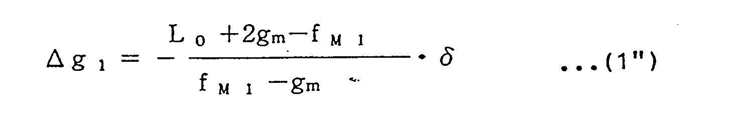


spots sensors zone plates 61 and 71; and 62 and 72, a slight change in the surface spacing gm between the mask and the wafer causes only a small amount of change in the spacing between thespots sensors 


spots - A particular example of this will be explained below. If,
- fM1 = 253.85 microns
- fM2 = 114.535 microns
- Δ1 = Δ2 = 10 microns
- Lo = 18345.94 microns
- On the other hand, the spacing g2, from the optical axis 102, of the
spot 82 resulting from the combination of patterns illustrated at part (B), namely, the combination ofpatterns 62 and 72, is such as follows:
- The relationship between g1+g2 and gm is such as follows:

- Further, when the surface spacing gm is maintained constant at a value 71.5 microns and if there occurs a
positional deviation 8 between the mask and the wafer, then gi and g2 are such as follows:
- Namely, if there occurs a
positional deviation 8 between the mask and the wafer in the X-Y plane, the spacing between thespots sensors spots sensors - As compared therewith, if the gap between the mask and the wafer changes by 5 microns, from 71.5 microns to 66.5 microns, the change in the spacing between the
spots resolution 2 micron and can be disregarded without causing inconveniences. The spacing "|1 + (g1 +g2)" between thesespots spots - Since each of the Fresnel zone plate 61 - 63 and 71 - 73 shown in Figure 5 has a lens function in respect to both the X direction and the Y direction, any relative displacement between the
mask 2 and thewafer 3 in the Y direction causes displacement of thespots line sensor line sensors mask 2 and thewafer 3 in the Y direction, any one of thespots line sensor 4 or 6, such as, for example, an FZP having a diffraction function like that of a cylindrical lens. In such case, if the mask and the wafer are relatively deviated in the Y direction which is perpendicular to the lateral deviation detecting direction (the lengthwise direction of the line sensor, i.e., X direction), thespots sensors - As described hereinbefore, the combination of FZP patterns illustrated in Figures 4 and 5 is provided on the mask and wafer, and by using part (A) and (B) any lateral positional deviation can be detected while, on the other hand, by using parts (B) and (C), the spacing can be measured. The spacing detection has substantially no dependence upon the lateral positional deviation and, on the other hand, the detection of lateral positional deviation has substantially no dependence on the spacing. Additionally, both the alignment detection and the surface spacing detection can be made at high precision. Further, if there occurs wafer tilt (inclination of wafer), since the detection of any positional deviation in the X-Y plane and the detection of the surface spacing are based on the information regarding the spacing of two spots, the spacing of these spots does not change by the wafer tilt. Therefore, the wafer tilt does not result in a detection error.
- Further, if the light projecting system (light source 1a in this example) for the inputted
light 1 or the alignment and gap detecting system, holding thesensors mask 2 and thewafer 3, there does not occur an error because any positional deviation in the X-Y plane (lateral positional deviation) is detected on the basis of the spacing between thespots spots - Figure 6 illustrates, as an example, the relationship between (i) pattern areas for the patterns of the mask and the wafer, when the mask and the wafer are aligned with each other, and (ii) those lines which contain the optical axes of the patterns and which are in parallel to the Y axis (in this example, the lines 61a, 62a, 6aa, 71a, 72a and 73a). Actually the pattern areas of the mask and the wafer are superposed in respect to the Z direction. However, in Figure 6, they are illustrated as being relatively shifted in the Y direction, for convenience in illustration.
- Figure 7, parts (A) and (B), illustrates examples of the manner of formation of
signal spot lights spots spots - Figure 9 illustrates another embodiment. In part (A) of Figure 9, the diffraction function of each FZP is such that: an FZP 121 on the mask has a diverging function and an FZP 131 on the wafer has a converging function. In part (B), an FZP 122 on the mask has a converging function and an FZP 132 on the wafer has a diverging function. In part (C), an FZP 123 on the mask has a converging function and an FZP 133 on the wafer has a diverging function. Considering these zone plates as lenses, part (A) corresponds to a combination of concave and convex lenses, part (B) corresponds to a combination of convex and concave lenses, and part (C) corresponds to a combination of convex and concave lenses. The optical axes 151, 152 and 153 of the patterns of the Fresnel zone plates on the wafer are set to be shifted relatively to and in parallel to the optical axes 141, 142 and 143 of the Fresnel zone plates of the mask, by Δ1*,O2* and Δ3 * in the illustrated direction.
- Where g1 *, g2 * and g3* denote the distances of spots 161, 162 and 163 formed on the
sensors 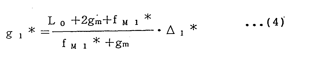


- Therefore, in a similar manner as in the embodiment described with reference to Figures 4 and 5, it is possible to detect any deviation between the mask and the wafer in the X-Y plane (i.e. lateral positional deviation) by detecting the spacing between the sots 161 and 162 by using detection systems shown in parts (A) and (B), while it is possible to measure the surface spacing gm between the mask and the wafer by detecting the spacing between the spots 162 and 163 by using the detection systems shown in parts (B) and (C).
- Figure 10 shows another embodiment wherein each of Fresnel zone plates 171, 172 and 173 of a mask has a refracting function in respect to the X direction, in addition to the light converging (or diverging) function. In this case, the spacing between (i) a spot 211 formed on a
photodetector 5 by the combination of patterns of the FZP 171 and an FZP 181 and (ii) a spot 212 formed on aphotodetector 4 by a combination of patterns of the FZP 172 and an FZP 182, is used for the detection of any positional deviation (lateral positional deviation) between the mask and the wafer in the X-Y plane. On the other hand, the spacing between spots 213 and 212 formed on thephotodetector 4 by the combination of patterns of the FZP 173 and an FZP 183, is used for the detection of the surface spacing between the mask and the wafer. In this case, as shown in Figure 10, the patterns 17i -173 of the mask are designed so that their focal point positions Fi, F2 and F3 are made eccentric as illustrated in Figure 10 by ε1,ε2 and ε3 with respect to the optical axes 191, 192 and 193 of these patterns. The respective focal lengths are denoted by f M1, f M2 and f M3. Reference numerals 201, 202 and 203 and denote the optical axes of the zone plates 181, 182 and 183, respectively. The spots of lights from the FZP patterns of the mask and the wafer are formed on thesensors optical axes 191, 192 and 193 of the mask patterns 171, 172 and 173, respectively, in the directions and at positions as illustrated in Figure 10. Here,


- Also in this case, by using the relations given by equations (7), (8) and (9), the lateral positional deviation (deviation in the X-Y plane) is detected on the basis of the combination of detection systems (A) and (B) while the surface spacing is measured on the basis of the combination of the detection systems (B) and (C), like the embodiments shown in Figures 4 and 9.
- In each of the embodiments described hereinbefore, three sets of FZP patterns are provided on a mask and a wafer, and one of these sets is used both for the detection of lateral positional deviation and for measurement of the surface spacing. Each of the other two sets is used only for the detection of the lateral positional deviation or for the measurement of the surface spacing. For example, in the embodiments shown in Figures 4, 9 and 10, a set of Fresnel zone plates of the mask and the wafer as illustrated in part (B) are used both for the detection of lateral positional deviation and for detection of the surface spacing. On the other hand, the set of mask and wafer Fresnel zone plates shown in part (A) are used for detection of the lateral position, whereas a combination of the mask and wafer Fresnel zone plates shown in part (C) are used for the detection of the surface spacing. In practical use, it is sufficient that at least one set of mask and wafer patterns are used in common for the detection of an alignment error and for detection of the surface spacing. Further, the disposition of pattern area on the mask is not limited to the example shown in Figure 6.
- For example, in regard to the division of the pattern area on the mask and the wafer, there are many possible varieties an example of which is illustrated in Figure 11. In the Figure 11 example, reference numeral 221, 222 and 223 denote FZP pattern areas on a
mask 2, while reference numerals 231, 232 and 233 denote FZP pattern areas on a wafer. The portions 221 and 231 are used in a pair, the portions 222 and 232 are used in another pair, and the portions 223 and 233 are used in a further pair. The mask-to-wafer alignment can be detected on the basis of the spacing between a light spot formed by the combination 221 and 231 and a light spot formed by the combination 222 and 232, on the sensor surface. On the other hand, the surface spacing between the mask and the wafer can be detected on the basis of the spacing between a light spot formed by the combination 222 and 232 and a light spot formed by the combination 223 and 233, on the sensor surface. Those lines denoted at 221a, 222a, 223a, 231a, 232a and 23aa, parallel to the Y axis and containing the respective principal axes of respective FZP pattern areas, are in such positional relationship as illustrated. - Figures 12, 13 and 14 show another embodiment, wherein Figure 12 is a perspective view and Figure 13 is a representation of the device as viewed in a direction (Y direction) perpendicular to the lengthwise direction of lines of
sensors wafer 3 surface and, by means of the FZP patterns 243 and 253 provided on the mask, the light spot 283 to be used for detection of the mask-and-wafer surface spacing is produced. - In Figure 13, the patterns 251 and 252 on the wafer have their optical axes shifted by Δ1' and Δ2' from the axes of the patterns on the mask, in the directions as illustrated. Also, the axes of the patterns 243 and 253 on the mask are mutually deviated by A3', while retaining the parallel relationship. Where the light spots 281, 282 and 283 formed on the
sensors 


- As determined by equations (10), (11) and (12) and for the reason the same as that having been described with reference to the embodiment shown in Figure 4, with the device shown in Figures 12 -14 it is possible to execute detection of lateral positional deviation and measurement of surface spacing, without being affected by any inclination of the wafer. As described with reference to the present embodiment, the measurement of the surface spacing between a mask and a wafer can be made without a pattern on the wafer, by using zero-th order reflection light from the wafer. However, it is a possible alternative that, as shown in Figure 15, a straight grating 254 is provided in an area on the
wafer 3, having no pattern, so that only a reflecting action is applied by the wafer to the light having been diffracted by the pattern area 243 of the mask, for enhancement of the efficiency of impingement of light to the area 253 on the mask. - The foregoing description has been made to examples wherein a mask and a wafer are disposed close to each other. However, the invention is applicable also to steppers (step-and-repeat type exposure apparatuses) such as an optical stepper or an excimer laser stepper that uses an excimer laser. Examples will now be explained with reference to Figures 16 and 17.
- In Figure 16, denoted at 1 is a light which illuminates FZP patterns 351, 352 and 353 provided on a
reticle 2, and denoted at 321, 322 and 323 are FZP patterns provided on a wafer.Numeral 30 denotes an imaging lens. The lights diffracted by the patterns (FZPs) 321,322 and 322 on the wafer are converged to form spots 331, 332 and 333 onsensors sensors imaging lens 30, it is directed outwardly of the imaging optical system and then is received by the sensor. - Figure 17 shows an example wherein the invention is applied to a mirror projection type stepper.
Reticle 2 andwafer 3 are disposed in an optically conjugate (imaging) relationship, with respect to three groups ofmirrors reticle 2, and numerals 441, 442 and 443 denote FZP patterns provided on thewafer 42. These patterns are structured in accordance with the same principle as of the Figure 4 embodiment. By measuring the spacings of spots 491, 492 and 493 formed on asensor 9, it is possible to detect any deviation in X-Y plane of the mask and the wafer (i.e. lateral positional deviation) and to detect the surface spacing between them. The principle of detection is the same as of the foregoing embodiment. - Figure 18 illustrates a modified form of the Figure 4 embodiment. In this example, the combination of
patterns 61 and 71; and 62 and 72, illustrated at parts (A) and (B) of Figure 4 is used as it is and the alignment error is detected in the same principle as that of the Figure 4 embodiment. As contrasted, with regard to the spacing between the mask and the wafer, in this example, it is detected on the basis of the position of aspot 82 on thesensor 4 surface. This will be explained in more detail. - First, as a mask is initially set in the apparatus, a reference position of the spot 82 (i.e., the position as assumed when the mask and the wafer have no relative positional deviation and also they are set at a correct spacing) is determined. This can be done on the basis of trial printing, for example. Since values Lo, fM2 and A can be predetermined from design values, the position of the optical axis of the FZP 62, on the surface of the
sensor 4, can be determined in accordance with equation (2'). In the actual spacing measuring operation, first the alignment error is detected in accordance with the principle described hereinbefore and, subsequently, the detected alignment error is corrected to reduce the same to zero. Then, any deviation of thespot 82 at that time from the optical axis position is measured by using thesensor 4 to obtain g2 and, thereafter, from equation (2') a current spacing gm is detected. - Figure 19 illustrates another modified form of the Figure 4 embodiment. In this example, the combination of
patterns spot 82 on thesensor 4 surface. This will be explained in greater detail. - As a mask is initially set in the apparatus, like the Figure 18 embodiment, the reference position as well as the correct spacing gm are detected. Then, in the actual position detecting operation, a current spacing is measured in accordance with the principle described hereinbefore, and subsequently, any error is corrected to establish the correct spacing. Any deviation of the
spot 82 at that time from its reference position is measured to obtain Ag2 and, from equation (2") thealignment error 8 is detected. - Figure 20 is a perspective view of a major part of a ninth embodiment of the present invention. Figures 21 and 22 are shematic representations of the major part of the device, as viewed in a direction which is perpendicular to the alignment detecting direction and which is parallel to first and second objects, the optical paths being illustrated in an unfolded state. Figures 21 and 22 are different, in respect to the spacing between the first and second objects.
- In Figure 20, denoted at 1 is a light supplied from a light source such as, for example, an He-Ne laser or a semiconductor laser. Denoted at 2 is a first object which is a mask, for example, and denoted at 3 is a second object which is a wafer, for example. The
mask 2 and thewafer 3 are disposed opposed to each other with a spacing gAF (Figures 20 and 21) or a spacing gAA (Figure 22) maintained therebetween. Numerals 1061, 1062 and 1063 denote first, second and third physical optic elements each being provided in a portion of amask 2. Numerals 1071, 1072 and 1073 denote first, second and third physical optic elements each being provided in a portion of the water. Each of these physical optic elements 1061 - 1063 and 1071 -1073 is formed, for example, by a diffraction grating or a Fresnel zone plate (which hereinafter will be referred also to simply "FZP"). - Figure 23 shows examples of patterns for the physical optic elements 1061 -1063 and 1071 - 1073 to be provided on the
mask 2 and thewafer 3. - Denoted at 4 and 5 are first and second light receiving means (sensors) each comprising a line sensor or a position sensing diode (PSD), for example, and each being adapted to detect, for example, the position of center of gravity of each inputted light 1081,1082 or 1083.
Signal processing circuit 9 is adapted to process the signals from the light receiving means 4 and 5 to detect, for example, the position of center of gravity of each light 1081, 1082 or 1083 incident on the light receiving means 4 or 5. Also, the signal processing circuit is adapted to determine, by calculation, any positional error δ and the spacing do, between themask 2 and thewafer 3. - In this embodiment, light I (whose wavelength λ = 830 nm, for example) from a semiconductor laser LD is incident on the first, second and third Fresnel zone plates 106i, 1062 and 1063 on the
mask 2, at an angle 6. Diffraction lights of a predetermined order or orders, diffracted perpendicularly from themask 2, are reflectively diffracted by the FZP patterns 1071,1072and 107 on thewafer 3 surface. Those of the diffraction lights of a predetermined order or orders, reflectively diffracted by the FZP patterns 1071 -1073 on thewafer 3, which pass themask 2 without being affected thereby (i.e in the form of zero-th order transmission light), are received by the light receiving means 4 and 5. Here, the positions of the gravity center of the inputtedlights 108i, 1082 and 1083, incident on the surfaces of the light receiving means 4 and 5, are detected by these light receiving means 4 and 5. By using output signals from the light receiving means 4 and 5, thesignal processing circuit 9 calculates the amount of positional error between themask 2 and thewafer 3 as well as the surface spacing between them. - The present embodiment uses three detection systems, i.e., a detection system A comprising first physical optic elements 1061 and 1071; a detection system B comprising second physical optic elements 1062 and 1072; and a detection system C comprising the third physical optic elements 1063 and 1073, provided on the
mask 2 and thewafer 3. Of these detection systems, the detection system A and the detection system B cooperate to provide a positional deviation detecting system. The detection system B is used in common, and the detection systems B and C cooperate to provide a surface spacing detecting system. - In regard to the light converging or diverging effect of the Fresnel zone plates shown in Figures 21 and 22, each of the FZP patterns 1061, 1072 and 1073 has a converging, positive power, while each of the FZP patterns 1062, 1063 and 1071 has a diverging, negative power. The Fresnel zone plate is not limited to one having a refracting or diverging function only in respect to the alignment direction. Namely, in this embodiment, such a Fresnel zone plate as having two-dimensional refracting or diverging function is usable.
- In the Figure 22 example, the
mask 2 and thewafer 3 are disposed close to each other (the surface spacing is 5 -100 microns, for example), as that the arrangement is suitably incorporated into what can be called an "X-ray stepper" wherein the exposure is made by using X-rays. - Usually, in an X-ray stepper, an exposure area per one exposure using X-rays is of a size 10 to several tens millimeters square, and while intermittently shifting the
wafer 3 position, exposures of twenty (20) to several tens shots are made. - For this reason, in many cases, the spacing between a mask and a wafer at the time of relative movement of them, for each shot, differs from the spacing between the mask and the wafer as measured just before the initiation of the exposure operation through a positional deviation detecting system (auto alignment system).
- The surface spacing illustrated in Figure 22 is one as assumed at the time of autoalignment, and it is of an order of 5 -100 microns as described hereinbefore. As compared therewith, the surface spacing illustrated in Figure 21 is one as assumed at the time of wafer movement, and it is large, of a value of 50 - 200 microns.
- As described, the surface spacing at the time of wafer movement is set to be large. This is made so as to prevent contact of the wafer with the mask surface during movement of the former along the X-Y plane, due to any surface height irregularity to tilt (inclination) of the wafer.
- The spacing 9AF in Figure 21 is one for which the mask and the wafer are set for execution of the wafer movement (shot area movement) and, in this state, the actual spacing between the mask and the wafer is detected. This is called "autofocusing". The spacing gAA shown in Figure 22 is one for which the mask and the wafer are set for execution of detection of any positional deviation therebetween (autoalignment), the mask and the wafer being set to this spacing on the basis of the measurement of the surface spacing as the mask and the wafer are placed at the spacing gAF in Figure 21.
- Next, description will be made of the position of incidence and the spot diameter of each inputted light 1081, 1082 or 1083 on the light receiving means 4 or 5.
- It is now assumed for convenience that in Figure 21 the
mask 2 and thewafer 3 have relative positional deviation of anamount 8 in respect to a vertical direction as viewed in the sheet of the drawing. Also, it is assumed that the light spots 1081, 1082 an 1083 formed on thesensors mask 2, respectively.Numerals - The powers of the Fresnel zone plates 1061, 1071, 1062 and 1072 of the mask and the wafer are so set that, when the mask and the wafer is at the spacing gAA, spots 1081 and 1082 of smallest diameter are formed on the
sensor 5. Also, the arrangement is such that, when the mask and the wafer is at the spacing gAF, a spot 1083 of smallest diameter is formed on the sensor 104. Accordingly, when the deviation between pattern optical axes of the mask and the wafer is equal to a distance δ' and the spacing between the mask and the wafer is equal to the spacing gAA, a diffraction spot 1081' provided by a detection system A, comprising the combination of the FZP patterns 1061 and 1071, has a smallest diameter; a diffraction spot 1082' provided by a detection system B, comprising the combination of the FZP patterns 1062 and 1072, has a smallest diameter; and a diffraction spot 1083' provided by a detection system C, comprising the combination of the FZP patterns 1063 and 1073, is expanded and has a large diameter, focusing at a point farther than thesensor 4. - In Figure 21, where fMi", fM2" and fM3" denote the focal lengths of the Fresnel zone plates 1061, 1062 and 1063, respectively, in regard to first order diffraction light, and Lo denotes the surface spacing between the
mask 2 and theline sensors 


- Also, in Figure 22, if the
mask 2 and thewafer 3 have relative positional deviation of an amount 8', the distances yi', y2' and y3' of the positions of the gravity centers of the light spots 1081', 1082' and 1083', respectively, can be written as follows:


- Here, each FZP on the mask or wafer has a pattern such as shown in Figure 23, for example, and each pattern on the wafer is provided in a scribe line. Due to the diffraction effect of each of the Fresnel zone plates 1061 and 1071; 1062 and 1072; and 1063 and 1073, a change in the gap between the
mask 102 and thewafer 103 causes a change in the diameter of each spot of thesensor sensor sensor 5 of a spot of light diffracted by the detection system B, comprising a combination of the FZP patterns 1062 and 1072, as well as the half width on thesensor 4 of a spot of light diffracted by the detection system C, comprising a combination of the FZP patterns 1063 and 1073, are set such as shown in Figure 24. - Here, the state of spots on the
sensors - It is now assumed that Lo = 18345.94 microns; gAF = 71.5 microns; gAA = 30 microns; the diffraction by the combination of FZP patterns 1061 and 1071 is effective to form a smallest spot on the sensor when the spacing is equal to gAA; and the displacement yi' of a spot on the sensor surface is of an amount one-hundred (100) times larger than the deviation 8' between the mask and the wafer.
- The diffraction by the combination of FZP patterns 1062 and 1072 is set so that the spot on the sensor surface becomes smallest when the spacing is equal to gAA. The displacement of the spot on the sensor is of an amount one-hundred (100) times larger than the positional deviation between the mask and the wafer.
- The diffraction by the detecting system C, comprising the combination of FZP patterns 1063 and 1073, is set so that the spot on the sensor surface becomes smallest when the spacing is equal to gAF. Here,


- If the
deviation 8 = 8' = 2 microns, the relationship between the spacing and the distances y1, y2, y3, y1', y2' and y3', is such as follows:
- From the change in the spacing between the spots 1081' and 1082', the position deviation (alignment error) between the mask and the wafer is detectable. As set forth in the numerical example, a deviation between the mask and the wafer of an
amount 2 microns causes a change in the spacing between the light spots 1081' and 1082' on the sensor surface by 400 microns. (Particular note should be paid to the values of the distances yi' and Y2'.) The spacing between the mask and the wafer is measured, not by measuring the spacing between the spots 1082 and 1083 on the sensor surface, but by measuring the size of each of the spots 1082 and 1083, in the manner described with reference to Figure 24. - Actually, as illustrated in Figure 26B, on the
line sensors 
- ii: the number of a smallest address of the bits providing the spot distribution; and
- if: the number of a largest address of the bits providing the spot distribution.
- The positions of the gravity centers of the spots 1081, 1082 and 1083, determined in this manner are illustrated at M1, M2 and M3 in Figure 26B, by way of example.
- Next, the calculation of the half width of the spot 1082 will be explained. Since usually a spot has an intensity distribution, like an Airy pattern called in the field of lenses, in this example, it is considered that the spot has such as distribution of intensity like that. For example, if a functional form of polynominal is applied to some bits, around the maximum output bit, of a line sensor, a maximum value in a spatially continuous output distribution on the sensor surface is obtainable from actually measured values of the output of these bits. When the maximum value is expressed by lmax, detection may be made to obtain a spatial value on the sensor that correspond to "lmax/2", from interruptedly changing outputs. Also, in such case, if the shape of the spot distribution is given by function approximation of polynominal and calculations are made to detect the value on the sensor that corresponds to "lmax/2", the half width of the light spot 1082 can be determined with a precision of an order of 1/10- 1/30 of the sensor bit size.
- As an example, in this embodiment, if the size of each of the FZP patterns 1061 -1063 and 1071 -1073 is about 50 microns x 90 microns, the spot diameter is about 200 - 800 microns. If the sensor bit size is about500 microns x 15 microns (pitch), the precision of detection of the half width of the spot can be 1 microns. Accordingly, by utilizing the characteristics that the spot half width changes such as shown in Figure 24, it is possible to detect the spacing between the mask and the wafer on the basis of detection of the half width of the spot 1082 and the half width of the spot 1083. While the relationship between the mask-and-wafer spacing and these half widths can be predetermined in accordance with design values, such relationship may be detected by experiments.
- In the present embodiment, as described hereinbefore, the detection system B which comprises a combination of Fresnel zone plates 1062 and 1072, is used both for the autoalignment and for the autofocusing. This allows that, with a relatively small pattern area surface such as shown in Figure 23, the two functions of autoalignment and autofocusing are provided. Further, in this embodiment, use is made of the fact that only the spacing between the spots 1081' and 1082' provides the information related to the positional deviation between the mask and the wafer, even if, as an example, the wafer is inclined or the relative positional relationship of the alignment detecting system (
sensors detection processing portion 9 in Figure 20) with the mask and the wafer changes slightly, the spots 1081' and 1082' on thesensor 5 changes by the same amount and the spacing itself between these spots is not affected by the wafer inclination or an error in the relative position of the detecting system with respect to the mask and the wafer. Therefore, stable detection is attained. - In the ninth embodiment shown in Figure 20, it is not always necessary that the
sensors sensor - In the ninth embodiment shown in Figure 20, the alignment (autoalignment) of the mask and the wafer is executed by using those Fresnel zone plates on the mask and the wafer having lens functions like a convex-concave system and a concave-convex system, while the detection of the surface spacing between the mask and the wafer (autofocusing) is executed by using a concave-convex system and a concave-convex system. However, the power arrangement may be set as desired.
- As an example, the autofocusing may be made by using a concave-convex system and a convex-concave system. Namely, in the present embodiment, any combination is usable provided that the focal lengths of the mask patterns and wafer patterns are adjusted and set so that the size of each of the spots, corresponding to the spots 1082 and 1083, changes with the spacing between the mask and the wafer.
- In place of the line sensors, a two-dimensional area sensor may be used for the
sensors - Figures 27 and 28 are schematic views, respectively, of a major part of a tenth embodiment of the present invention. Like Figures 21 and 22, Figures 27 and 28 show the optical paths, in an unfolded view, as the spacing between a first object (mask) 2 and a second object (wafer) 3 are changed, and these Figures show the device as viewed in a direction perpendicular to the alignment detecting direction.
- In the states shown in Figures 27 and 28, respectively, the alignment of the
mask 2 with thewafer 3 has been completed, such that no positional deviation is present therebetween. - In this embodiment, the autoalignment is executed by using a concave-convex system (detection system A) and a convex-concave system (detection system B), and is made by detecting the change in the spacing, on the sensor surface, between two spots obtained from these two detection systems. Also, the autofocusing is executed by using the convex-concave system (detection system B) and a convex-concave system (detection system C), and is made by detecting the size of each spot obtained from these two detection systems.
- In Figures 27 and 28, for the autoalignment, measurement is made to the spacing between a spot 1161' produced as a result of the diffraction at
Fresnel zone plates Fresnel zone plates spot 1162 produced as a result of the diffraction atFresnel zone plates Fresnel zone plates - In regard to the ninth and tenth embodiments, description has been made to examples wherein only one-dimensional detection is made for an alignment error (positional deviation). However, for actual alignment of a mask and a wafer in a plane, it is necessary to detect three parameters in the X, Y and 0 directions. If this is desired, as shown in Figure 29, patterns used in the foregoing embodiments (e.g. those shown in figure 23) may be provided outside a semiconductor circuit area 20 and at positions on a scribe line which is going to be used for the cutting, when it is on a wafer.
- In Figure 29, numerals 1181, 1182, 1183 and 1184 each denotes an FZP. The example shown in Figure 29 is of proximity type wherein a mask and a wafer are disposed close to each other. In this Figure, numerals 1191, 1192, 1193 and 1194 each denotes a detection system for executing the autoalignment or the autofocusing.
Numerals numerals - Where the detected values on the deviation as obtainable from these four detection systems are denoted by Δx1, Δy1, Ax2 and y2, it is sufficient for the detection of the positional deviation between the mask and the wafer to detect translational errors AX and AY and a rotational error Δθ. These errors can be easily determined from the four values (Δx1, Ax2, Δy1 and Δy2).
- Also, the spacing between the mask and the wafer is detected at the four points near the Fresnel zone plates 1181, 1182, 1183 and 1184.
- In accordance with the ninth and tenth embodiments as described hereinbefore, and detection of a three-dimensional positional error between a mask and a wafer as well as the positioning control for them based on the detection, can be done at high precision.
- Figure 30 is a perspective view of a major part of an eleventh embodiment of the present invention. In this embodiment, one of sets of diffraction patterns, from a mask and a wafer, each producing two spots for detection of the spacing between the mask and the wafer, uses zero-th order regular reflection by the wafer. That is, the present embodiment is an example wherein the wafer surface may have no pattern.
- In Figure 30,
numerals - In this embodiment, a pattern of a FZP 1243 is provided on the mask, and by detecting the spacing between (i) a spot obtainable by diffraction at a detection system A, comprising a combination of
FZP patterns 1231 and 1241, and (ii) a spot 1272 obtainable by diffraction at a detection system B, comprising a combination ofFZP patterns 1232 and 1242, the mask-to-wafer deviation (alignment error) is detected. On the other hand, the surface spacing (gap) between the mask and the wafer is detected by detecting the size of a spot 1272, on asensor 5 surface, obtainable by diffraction at the detection system B comprising the combination atFZP patterns 1232 and 1242, and the size of the spot 1273, on asensor 4 surface, obtainable by diffraction at a detection system C, comprising a combination ofFZP patterns 1233 and 1243. - The optical function of the remaining portion is the same as that of the ninth embodiment.
- By using the
Fresnel zone plates 1233 and 1243 provided on the mask, it is possible to reduce in size of the pattern area on the wafer. This is a significant feature of the present embodiment. - As illustrated in part (c) of Figure 31, the surface spacing between the
Fresnel zone plates 1233 and 1243 is equal to 2 x gAF, and the focal lengths and the imaging relationship of the patterns of these zone plates are set in consideration of it. - It is assumed in Figure 31 that the mask and the wafer have relative positional deviation of an amount A and, in that occasion, the centers of light spots (more exactly, chief rays of them) are at the positions of distances y 1, y and y 3, respectively, from the optical axes of the
FZP patterns 


- In accordance with the relations of equations (8), (9) and (10), the spacing between (i) a spot 1271 produced by the combination of
FZP patterns 1231 and 1241 (combined power of a concave-convex system) and (ii) a spot 1272 produced by a combination ofFZP patterns 1232 and 1242 (combined power of a convex- concave system) is calculated. Then, from the detected spacing, the positional deviation (alignment error) between the mask and the wafer is detected. - Each of the FZP patterns 1231 - 1233 and 1241 - 1243 has a lens function only in respect to the alignment detecting direction. However, it may have a lens function in respect to two-dimensional directions and, additionally, an area sensor may be used in place of the line sensors to detect the motion of each light spot. In regard to the change in the half width of each spot formed on a sensor surface by a combination of corresponding patterns, the setting is such that each of a spot produced by a combination of
FZP patterns 1231 and 1241 and a spot produced byFZP patterns 1232 and 1242, all being used for the autoalignment, becomes smallest when the spacing gAA is established; while a spot produced byFZP patterns 1233 and 1243 becomes smallest when the gap gAF is established. - In regard to the manner of change in the diameter of diffraction light spot on the
sensor - Here, depending on the value of the spacing, it is possible to measure the spacing on the basis of the magnitude of defocus of each of the three spots (i.e. spot size) formed by the three pattern combinations of the detection systems A, B and C. Therefore, it is possible to detect the spacing between the mask and the wafer, at higher precision.
- As an alternative, when a mask and a wafer are equipped with two sets of patterns which are used to provide detection systems A and B, the setting may be made so that the spot diameter of a sensor changes with the spacing between the mask and the wafer, in a manner as shown in Figure 33: wherein the detection system A may have a combined power of a convex-concave system or a concave-convex system, with a minimum spot being provided by a spacing near "2gAA - 2gAF"; and the detection system B may have a combined power of a concave-convex system or a convex-concave system, with a minimum spot being provided by a spacing gAF. Any positional deviation (alignment error) between the mask and the wafer can be detected on the basis of the spacing between a spot on a sensor formed by the pattern combination of the detection system A and a spot on a sensor formed by the pattern combination of the detection system B. On the other hand, the spacing between the mask and the wafer can be detected on the basis of the size of the spot on the sensor formed by the pattern combination of the detection system A as well as the size of the spot on the sensor formed by the pattern combination of the detection system B. As described, in this embodiment, it is possible to detect both of the positional deviation and the spacing, by using two lights.
- In regard to the setting of pattern areas on a mask and a wafer, in addition to the example shown in Figure 23, there are many possible variations of the manner of division thereof.
- An example is illustrated in Figure 34. In this Figure, a set of FZP patterns 1281 and 1291; a set of FZP patterns 1282 and 1292; and a set of FZP patterns 1283 and 1293 provide detection systems, respectively, producing respective spots.
- In respect to some embodiment above, description has been made to examples wherein a mask and a wafer are brought into alignment with each other while being maintained in a proximity relationship, such as in the case of an X-ray stepper. However, the invention is not limited to this, and it is applicable also to a stepper which uses a ultraviolet light or an excimer laser or a reduction imaging type exposure apparatus that uses mirrors, for example.
- Figure 35 is a schematic view of one embodiment wherein the invention is applied to a stepper that uses ultraviolet light or an excimer laser. In this Figure, denoted at 150 is a pattern illuminating light. Numerals 1351, 1352 and 1353 denote patterns provided on a
reticle 151 for alignment and autofocusing purpose.Numeral 130 denotes an imaging lens by which thereticle 151 and awafer 131 are brought into an optically conjugate relationship. In this embodiment, diffraction lights 1361, 1362 and 1363 fromalignment patterns wafer 131 go through theimaging lens 130 and are received by asensor 137. The spacings of thus producedspots processing system 134. By this, any positional deviation (alignment error) between the reticle and the wafer in a plane as well as any relative deviation therebetween in the direction of the optical axis of theimaging lens 130, can be detected. If, in this occasion, theimaging lens 130 shows chromatic aberration with respect to the usedlight 150, the patterns of the Fresnel zone plates 1351, 1352 and 1353 and the patterns of theFresnel zone plates - Figure 36 is a schematic view of one embodiment wherein the invention is applied to a reduction type stepper, using mirrors. In this example, a
pattern 143 on areticle 138 surface and apattern 144 on awafer 142 surface are used in the manner described with reference to the foregoing embodiments, to detect the spacing and size of spots 1491, 1492 and 1493 on a line sensor orarea sensor 146 to detect any positional deviation between thereticle 138 and thewafer 142 as well as any relative deviation therebetween in the direction of an optical axis of the optical arrangement constituted bymirrors - Also in the embodiments shown in Figures 35 and 36, the sensor may not be disposed at the illustrated plane but, in place thereof, a relay lens may be disposed at that position and the sensor may be placed in the imaging plane of the lens.
- Figure 37 shows a modified form of the Figure 20 embodiment. In this example, the combination of patterns 1061 and 1071; 1062 and 1072 shown in part (A) and (B) of Figure 2, is used as it is and the alignment error is detected essentially in the same principle as of the Figure 20 embodiment. On the other hand, the spacing between the mask and the wafer is detected only by using the diameter of a spot 1082, singly, on a
sensor 4. The relationship between the mask-and-wafer spacing and the spot diameter on the sensor, based on the combination of patterns 1062 and 1072, is such as illustrated in Figure 24. By detecting this relationship in preparation, it is possible to detect the mask-and-wafer spacing from the spot diameter. - Figure 38 shows another modified form of the Figure 20 embodiment. In this example, the combination of patterns 1062 and 1072; 1063 and 1073 illustrated in parts (B) and (C) of Figure 20, is used as it is and the mask-and-wafer spacing is detected essentially in the same principle as of the Figure 20 embodiment. In contrast, with regard to the alignment error between the mask and the wafer, in this example, it is detected on the basis of the position of a spot 1082 on a
sensor 4. This will be explained below. - As a mask is initially set in an apparatus, a reference position of the spot 1082 (i.e. the position thereof as assumed when the mask and the wafer have no relative positional deviation and they are set at a correct spacing gAA) is determined. This can be done by trial printing, for example. In the actual position detecting operation, first the spacing between the mask and the wafer is measured in accordance with the principle described hereinbefore, and, thereafter, any error in the spacing is corrected to set the mask and the wafer at the correct spacing. Then, any deviation of the spot 1082 at that time from its reference position is measured to obtain y2. Since values Lo and fM2" are predetected, from equation (511f) it is possible to obtain deviation 8'.
- In accordance with these embodiments, as described hereinbefore, for detection of relative positional deviation and surface spacing between first and second objects, a plurality of physical optic elements are provided on the first and second objects in a manner that a part thereof are used in common and, additionally, diffraction lights of a predetermined order or orders, not lower than first or second order, from these physical optic elements are used. This provides the following advantageous effects:
- (a) Since a part of the physical optic elements is used in common for the detection of positional deviation and the detection of surface spacing, only a small area is required for the pattern setting.
- (b) Since the positional deviation and the surface spacing can be detected with one light, a device as a whole can be made compact.
- (c) No error results from any inclination of the second object (wafer) or from an error in the setting of the detecting system. Therefore, high-detection is attainable.
- d) The positional deviation and the surface spacing can be detected simultaneously.
- While the invention has been described with reference to the structure disclosed herein, it is not confined to the details set forth and this application is intended to cover such modifications or changes as may come within the purposes of the improvements or the scope of the following claims.
then, the spacing g1, from the optical axis 101, of the

Claims (7)
Applications Claiming Priority (9)
| Application Number | Priority Date | Filing Date | Title |
|---|---|---|---|
| JP22580988 | 1988-09-09 | ||
| JP226006/88 | 1988-09-09 | ||
| JP22600688 | 1988-09-09 | ||
| JP225809/88 | 1988-09-09 | ||
| JP22600688 | 1988-09-09 | ||
| JP22580988 | 1988-09-09 | ||
| JP1209928A JP2581227B2 (en) | 1988-09-09 | 1989-08-14 | Position detection device |
| JP209928/89 | 1989-08-14 | ||
| JP20992889 | 1989-08-14 |
Publications (3)
| Publication Number | Publication Date |
|---|---|
| EP0358511A2 true EP0358511A2 (en) | 1990-03-14 |
| EP0358511A3 EP0358511A3 (en) | 1990-12-27 |
| EP0358511B1 EP0358511B1 (en) | 2001-07-18 |
Family
ID=27329069
Family Applications (1)
| Application Number | Title | Priority Date | Filing Date |
|---|---|---|---|
| EP89309094A Expired - Lifetime EP0358511B1 (en) | 1988-09-09 | 1989-09-07 | Device for detecting positional relationship between two objects |
Country Status (3)
| Country | Link |
|---|---|
| US (1) | US5148038A (en) |
| EP (1) | EP0358511B1 (en) |
| DE (1) | DE68929314T2 (en) |
Families Citing this family (4)
| Publication number | Priority date | Publication date | Assignee | Title |
|---|---|---|---|---|
| DE69128164T2 (en) * | 1990-05-01 | 1998-04-02 | Canon Kk | Method and apparatus for the detection of position deviations |
| JPH0563909A (en) * | 1991-08-28 | 1993-03-12 | Canon Inc | Color picture reader |
| JP3296239B2 (en) * | 1997-03-27 | 2002-06-24 | ウシオ電機株式会社 | Proximity exposure apparatus with gap setting mechanism |
| JP4707933B2 (en) * | 2000-11-27 | 2011-06-22 | ザ プロクター アンド ギャンブル カンパニー | Dishwashing method |
Citations (2)
| Publication number | Priority date | Publication date | Assignee | Title |
|---|---|---|---|---|
| GB2073950A (en) * | 1980-04-11 | 1981-10-21 | Western Electric Co | Method and apparatus for mask/wafer alignment |
| US4360273A (en) * | 1980-02-14 | 1982-11-23 | Sperry Corporation | Optical alignment of masks for X-ray lithography |
Family Cites Families (9)
| Publication number | Priority date | Publication date | Assignee | Title |
|---|---|---|---|---|
| US4037969A (en) * | 1976-04-02 | 1977-07-26 | Bell Telephone Laboratories, Incorporated | Zone plate alignment marks |
| US4539482A (en) * | 1980-10-09 | 1985-09-03 | Canon Kabushiki Kaisha | Reading apparatus |
| US4398824A (en) * | 1981-04-15 | 1983-08-16 | Bell Telephone Laboratories, Incorporated | Wafer tilt compensation in zone plate alignment system |
| US4629313A (en) * | 1982-10-22 | 1986-12-16 | Nippon Kogaku K.K. | Exposure apparatus |
| US4636626A (en) * | 1983-01-14 | 1987-01-13 | Nippon Kogaku K.K. | Apparatus for aligning mask and wafer used in semiconductor circuit element fabrication |
| US4545683A (en) * | 1983-02-28 | 1985-10-08 | The Perkin-Elmer Corporation | Wafer alignment device |
| US4514858A (en) * | 1983-03-15 | 1985-04-30 | Micronix Partners | Lithography system |
| US4656347A (en) * | 1984-01-30 | 1987-04-07 | Nippon Telegraph & Telephone Public Corporation | Diffraction grating position adjuster using a grating and a reflector |
| JPS61111402A (en) * | 1984-11-06 | 1986-05-29 | Nippon Kogaku Kk <Nikon> | Position detector |
-
1989
- 1989-09-07 DE DE68929314T patent/DE68929314T2/en not_active Expired - Fee Related
- 1989-09-07 EP EP89309094A patent/EP0358511B1/en not_active Expired - Lifetime
-
1991
- 1991-12-10 US US07/804,514 patent/US5148038A/en not_active Expired - Fee Related
Patent Citations (2)
| Publication number | Priority date | Publication date | Assignee | Title |
|---|---|---|---|---|
| US4360273A (en) * | 1980-02-14 | 1982-11-23 | Sperry Corporation | Optical alignment of masks for X-ray lithography |
| GB2073950A (en) * | 1980-04-11 | 1981-10-21 | Western Electric Co | Method and apparatus for mask/wafer alignment |
Non-Patent Citations (1)
| Title |
|---|
| JOURNAL OF VACUUM SCIENCE AND TECHNOLOGY: PART B. vol. B1, no. 4, October 1983, NEW YORK US pages 1276 - 1279; H. Kinoshita et al.: "A dual grating alignment technique for x-ray lithography" * |
Also Published As
| Publication number | Publication date |
|---|---|
| US5148038A (en) | 1992-09-15 |
| DE68929314D1 (en) | 2001-08-23 |
| DE68929314T2 (en) | 2002-05-02 |
| EP0358511A3 (en) | 1990-12-27 |
| EP0358511B1 (en) | 2001-07-18 |
Similar Documents
| Publication | Publication Date | Title |
|---|---|---|
| EP0409572B1 (en) | Position detecting system | |
| EP0411966B1 (en) | Position detection method and apparatus | |
| JP3570728B2 (en) | Lithographic projector with off-axis alignment unit | |
| US5200800A (en) | Position detecting method and apparatus | |
| EP0329430B1 (en) | Position detecting device | |
| US5204535A (en) | Alignment device having irradiation and detection light correcting optical elements | |
| EP0488798B1 (en) | Position detecting method | |
| EP0358514B1 (en) | Position detecting method and apparatus | |
| US5377009A (en) | Alignment method | |
| US5235408A (en) | Position detecting method and apparatus | |
| EP0439322B1 (en) | Device and method for measuring the gap between two opposed objects | |
| US5225892A (en) | Positional deviation detecting method | |
| US5495336A (en) | Position detecting method for detecting a positional relationship between a first object and a second object | |
| US5319444A (en) | Position detecting method and apparatus | |
| US5717492A (en) | Position detecting apparatus and a method for manufacturing semiconductor devices using the apparatus | |
| EP0336537A1 (en) | Device for detecting positional relationship between two objects | |
| US5294980A (en) | Positioning detecting method and apparatus | |
| EP0358425A2 (en) | Position detecting method and apparatus | |
| EP0358511A2 (en) | Device for detecting positional relationship between two objects | |
| EP0333326B1 (en) | Position detecting method and apparatus | |
| EP0358513B1 (en) | Position detecting method and apparatus | |
| EP0455446B1 (en) | Position detecting method and apparatus | |
| JP2546356B2 (en) | Alignment device | |
| JP2615778B2 (en) | Positioning device | |
| JP2513282B2 (en) | Alignment device |
Legal Events
| Date | Code | Title | Description |
|---|---|---|---|
| PUAI | Public reference made under article 153(3) epc to a published international application that has entered the european phase |
Free format text: ORIGINAL CODE: 0009012 |
|
| AK | Designated contracting states |
Kind code of ref document: A2 Designated state(s): DE FR GB NL |
|
| PUAL | Search report despatched |
Free format text: ORIGINAL CODE: 0009013 |
|
| AK | Designated contracting states |
Kind code of ref document: A3 Designated state(s): DE FR GB NL |
|
| 17P | Request for examination filed |
Effective date: 19901231 |
|
| 17Q | First examination report despatched |
Effective date: 19930706 |
|
| GRAG | Despatch of communication of intention to grant |
Free format text: ORIGINAL CODE: EPIDOS AGRA |
|
| GRAG | Despatch of communication of intention to grant |
Free format text: ORIGINAL CODE: EPIDOS AGRA |
|
| GRAH | Despatch of communication of intention to grant a patent |
Free format text: ORIGINAL CODE: EPIDOS IGRA |
|
| GRAH | Despatch of communication of intention to grant a patent |
Free format text: ORIGINAL CODE: EPIDOS IGRA |
|
| GRAA | (expected) grant |
Free format text: ORIGINAL CODE: 0009210 |
|
| AK | Designated contracting states |
Kind code of ref document: B1 Designated state(s): DE FR GB NL |
|
| PG25 | Lapsed in a contracting state [announced via postgrant information from national office to epo] |
Ref country code: FR Free format text: LAPSE BECAUSE OF FAILURE TO SUBMIT A TRANSLATION OF THE DESCRIPTION OR TO PAY THE FEE WITHIN THE PRESCRIBED TIME-LIMIT Effective date: 20010718 |
|
| REF | Corresponds to: |
Ref document number: 68929314 Country of ref document: DE Date of ref document: 20010823 |
|
| EN | Fr: translation not filed | ||
| REG | Reference to a national code |
Ref country code: GB Ref legal event code: IF02 |
|
| PLBE | No opposition filed within time limit |
Free format text: ORIGINAL CODE: 0009261 |
|
| STAA | Information on the status of an ep patent application or granted ep patent |
Free format text: STATUS: NO OPPOSITION FILED WITHIN TIME LIMIT |
|
| 26N | No opposition filed | ||
| PGFP | Annual fee paid to national office [announced via postgrant information from national office to epo] |
Ref country code: GB Payment date: 20030826 Year of fee payment: 15 |
|
| PGFP | Annual fee paid to national office [announced via postgrant information from national office to epo] |
Ref country code: DE Payment date: 20030919 Year of fee payment: 15 |
|
| PGFP | Annual fee paid to national office [announced via postgrant information from national office to epo] |
Ref country code: NL Payment date: 20030930 Year of fee payment: 15 |
|
| PG25 | Lapsed in a contracting state [announced via postgrant information from national office to epo] |
Ref country code: GB Free format text: LAPSE BECAUSE OF NON-PAYMENT OF DUE FEES Effective date: 20040907 |
|
| PG25 | Lapsed in a contracting state [announced via postgrant information from national office to epo] |
Ref country code: NL Free format text: LAPSE BECAUSE OF NON-PAYMENT OF DUE FEES Effective date: 20050401 Ref country code: DE Free format text: LAPSE BECAUSE OF NON-PAYMENT OF DUE FEES Effective date: 20050401 |
|
| GBPC | Gb: european patent ceased through non-payment of renewal fee |
Effective date: 20040907 |
|
| NLV4 | Nl: lapsed or anulled due to non-payment of the annual fee |
Effective date: 20050401 |