EP0357616B1 - Process and device for compensating errors of measurement - Google Patents
Process and device for compensating errors of measurement Download PDFInfo
- Publication number
- EP0357616B1 EP0357616B1 EP88902462A EP88902462A EP0357616B1 EP 0357616 B1 EP0357616 B1 EP 0357616B1 EP 88902462 A EP88902462 A EP 88902462A EP 88902462 A EP88902462 A EP 88902462A EP 0357616 B1 EP0357616 B1 EP 0357616B1
- Authority
- EP
- European Patent Office
- Prior art keywords
- signal
- analog
- compensation
- input
- voltage
- Prior art date
- Legal status (The legal status is an assumption and is not a legal conclusion. Google has not performed a legal analysis and makes no representation as to the accuracy of the status listed.)
- Expired - Lifetime
Links
Images


Classifications
-
- H—ELECTRICITY
- H01—ELECTRIC ELEMENTS
- H01L—SEMICONDUCTOR DEVICES NOT COVERED BY CLASS H10
- H01L21/00—Processes or apparatus adapted for the manufacture or treatment of semiconductor or solid state devices or of parts thereof
- H01L21/02—Manufacture or treatment of semiconductor devices or of parts thereof
- H01L21/04—Manufacture or treatment of semiconductor devices or of parts thereof the devices having at least one potential-jump barrier or surface barrier, e.g. PN junction, depletion layer or carrier concentration layer
- H01L21/50—Assembly of semiconductor devices using processes or apparatus not provided for in a single one of the subgroups H01L21/06 - H01L21/326, e.g. sealing of a cap to a base of a container
- H01L21/56—Encapsulations, e.g. encapsulation layers, coatings
-
- G—PHYSICS
- G01—MEASURING; TESTING
- G01D—MEASURING NOT SPECIALLY ADAPTED FOR A SPECIFIC VARIABLE; ARRANGEMENTS FOR MEASURING TWO OR MORE VARIABLES NOT COVERED IN A SINGLE OTHER SUBCLASS; TARIFF METERING APPARATUS; MEASURING OR TESTING NOT OTHERWISE PROVIDED FOR
- G01D3/00—Indicating or recording apparatus with provision for the special purposes referred to in the subgroups
- G01D3/02—Indicating or recording apparatus with provision for the special purposes referred to in the subgroups with provision for altering or correcting the law of variation
- G01D3/022—Indicating or recording apparatus with provision for the special purposes referred to in the subgroups with provision for altering or correcting the law of variation having an ideal characteristic, map or correction data stored in a digital memory
-
- G—PHYSICS
- G01—MEASURING; TESTING
- G01L—MEASURING FORCE, STRESS, TORQUE, WORK, MECHANICAL POWER, MECHANICAL EFFICIENCY, OR FLUID PRESSURE
- G01L1/00—Measuring force or stress, in general
- G01L1/20—Measuring force or stress, in general by measuring variations in ohmic resistance of solid materials or of electrically-conductive fluids; by making use of electrokinetic cells, i.e. liquid-containing cells wherein an electrical potential is produced or varied upon the application of stress
- G01L1/22—Measuring force or stress, in general by measuring variations in ohmic resistance of solid materials or of electrically-conductive fluids; by making use of electrokinetic cells, i.e. liquid-containing cells wherein an electrical potential is produced or varied upon the application of stress using resistance strain gauges
- G01L1/2268—Arrangements for correcting or for compensating unwanted effects
- G01L1/2281—Arrangements for correcting or for compensating unwanted effects for temperature variations
-
- H—ELECTRICITY
- H01—ELECTRIC ELEMENTS
- H01L—SEMICONDUCTOR DEVICES NOT COVERED BY CLASS H10
- H01L2924/00—Indexing scheme for arrangements or methods for connecting or disconnecting semiconductor or solid-state bodies as covered by H01L24/00
- H01L2924/0001—Technical content checked by a classifier
- H01L2924/0002—Not covered by any one of groups H01L24/00, H01L24/00 and H01L2224/00
Definitions
- the invention relates to a method for compensating and / or shaping external measurement signals by means of an analog-digital converter which can be operated in the dual slope method, and to an associated device for signal compensation and / or shaping according to claims 1 and 6.
- a method for measuring error compensation which is improved compared to the last-mentioned prior art has become known from EP-A 0 169 414.
- the measuring method known therefrom or the corresponding device for carrying out the measuring method comprises a compensation circuit operating in digitized form.
- the measurement signals obtained in analog fashion are further processed in an analog manner, with an analog measurement signal being digitized only in a control circuit, in order to then call up correspondingly pre-stored, digitized compensation and signal shaping values obtained on the basis of calibration and to return them to the measurement circuit.
- the compensation, correction and / or signal shaping is carried out during the digitization of the analog measurement signals, for which purpose compensation, correction and / or signal shaping signals are fed to the analog-digital converter as the control operating variables influencing them and are transmitted to the analog-digital Analog measuring signals applied to the converter are processed in such a way that a modified digitized output signal which is dependent on the compensation, correction or signal shaping values is present at the output of the analog-digital converter.
- An analog-digital converter is basically also from the previously published publication "Electronic Engineering”, vol. 55, No. 680, August 1983 (London, GB), J. Lacy et al .: “Enhancing the dynamic range of an A / D converter", pages 49-52, 57.
- the object of the present invention is therefore to provide a method and a device for measuring error compensation, correction and / or signal shaping, which makes it possible, in particular in the case of piezoresistive sensors, to digitize a measuring signal with the highest accuracy and accuracy, with zero point compensation also simple and effective means should be feasible.
- the present invention proposes, for the first time, a microprocessor-controlled analog-digital converter which operates according to the dual slope method and with which zero point compensation is possible not only for deviations in internal circuits, but above all for deviations in the external measurement signal.
- a compensation of the signal shaping is carried out taking into account the above special features during the analog-digital conversion. Appropriate compensation and signal shaping before conversion would otherwise require additional amplification of the original measurement signal, which on the one hand requires high power consumption and on the other hand leads to an additional, uncorrectable error.
- a compensation of the measurement signal after a corresponding signal shaping and after an analog-digital conversion would ultimately lead to a circumcision of the original measurement signal which can no longer be corrected, with a loss of errors and information.
- the dual slope method is particularly suitable here because a combination can be carried out in three ways, namely once in a rest phase by a level or level shift, in the negative edge phase by preselectable setting and change in the phase duration T of the input Signal integration, and in the subsequent positive edge phase by preselectable setting and changing the reference voltage to be integrated.
- the microprocessor-based structure also enables a so-called master-slave mode of operation, via which a connected microprocessor can also be controlled.
- the device can also be operated in the so-called stand-alone mode or even in a "cascade arrangement" in which several devices are linked to one another via a microbus.
- the integrated microprocessor Due to the programmable structure of the analog-digital conversion signal adaptation processing, any adaptation to specific technical requirements is possible, and the integrated microprocessor can also be used to calculate and implement any compensation values between two stored values, which is particularly advantageous when measuring the calibration values is because this means that only relatively few calibration points can be measured and intermediate values can be interpolated under computer control.
- the resolution can also be easily programmed in any ratio and thus a desired curve fitting (signal fitting) can be carried out.
- a preferred construction of the device takes the form of a microchip which can be connected to a computer via a microbus interface. Via the microprocessor contained on the chip, the compensation values programmed, processed and processed can be called up via the Interbus then the programmable analog-to-digital converter adapter (PADCAS), which in turn automatically performs the signal compensation during the analog-to-digital conversion.
- PIDCAS programmable analog-to-digital converter adapter
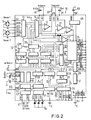
- FIGS. 1 and 2 in which a basic block diagram with the associated connection diagrams are shown.
- the device then consists of a signal processing circuit 1, which is designed as a semiconductor chip.
- An electrical erasable and programmable read-only memory EEPROM 4 can be connected to this via a first interface 2.
- the signal processing circuit 1 can also be connected to an external microprocessor or microbus via a further interface 3.
- the connections or actuatable switches named in FIG. 1 by means of letter and / or number combinations are explained and listed by the table reproduced in the system, to which reference is made in this respect.
- two sensors 5 and 7 can be connected.
- the sensors can alternatively, for example even nested, and thus be operated simultaneously with a time delay, e.g. B. in a reference pressure gauge.
- the supply voltage V CC is present at the VDDA / VDDD inputs and at the GNDA / GNDD ground connection.
- the sensor bridge current supply can be set and preselected in 16 programmable individual steps via a four-bit register decoder 9 and a downstream current source selector stage 11, which can be optionally connected to the respective measuring bridge of the first or second sensor via the inner current source 12 and a first multiplexer 13 5 or 7 can be created.
- These 16 differently programmable current levels are also used to set the sensor in an eight-bit analog-digital range if the temperature is measured by digital / analog comparison on the measuring bridge.
- the programmable current source is also used to adjust the sensor signal with regard to the desired output voltage range. Furthermore, temperature compensation is possible, which will be explained later.
- the voltages are applied to the respective sensor 5 or 7 via the connections TS1 or TS2 (Top of Sensor) and the opposite ground connection on the bridge.
- the measured signal taken transversely to the measuring bridge is fed via the connections CH1H (Channel 1 High) and CH1L (Channel 1 Low) to the first multiplexer 13 and via a further multiplexer 15 to a buffer 17 as a buffer.
- An integrator stage 21 and then the comparator stage 23 for forming an analog-digital converter 19, also called ADC for short, are connected downstream of the output of the buffer memory 17.
- the AD converter which works according to the so-called double integration method (dual mode), is described below.
- the input of the integrator 21 is connected to the output of the buffer memory 17 via an input resistor 22 (in the exemplary embodiment 27 KOhm).
- a capacitor 24 (33 nF in the exemplary embodiment) is also connected between the input and output of the OP amplifier 21.
- the output of the integrator leads to a comparator 23, the output of which is connected to a master control logic 25, hereinafter also referred to as MCL for short.
- MCL master control logic
- a four-bit-wide bidirectional bus is provided in the exemplary embodiment shown, the bits being shiftable cyclically via four-bit registers .
- a connection from the internal bus of the signal processing circuit 1 via the interface 3 to a connection to an external microprocessor or external data processing is possible via a microprocessor connection 27 as an input-output connection via a D0-D3 channel 29.
- Interface 3 is also the address register enable pulse ALE (ALE-STROBE), the read input pulse RD (Read Strobe) assigned for bus reading and the write input pulse WR (Write Strobe) for bus writing.
- ALE address register enable pulse
- the read input pulse RD Read Strobe
- WR Write Strobe
- the pending 4-bit input value from DO-D3 channel 29 is read into address memory 31, which in turn activates the selected D memory for subsequent writing or reading via MCL logic.
- the RD strobe pulse the output signal present at its output due to the corresponding activation of the D memory is present on the DO-D3 channel 29.
- Two four-bit instruction registers 31 are also provided in the signal processing circuit 1 as internal logic. These registers are written with a four-bit logic control word LCW. These four-bit LCW words are then decoded by two, 16 from 4-bit command word decoders and converted into output signals which switch individual control blocks of the MCL master control logic 25. Each LCW command word remains pending until another change occurs.
- an eight-bit digital / analog converter with a resistor chain is also provided in addition to the voltage supply selection stage 11 which can be programmed in 16 steps.
- the DA converter 33 is used not only for temperature measurement, but also additionally for signal compensation, namely once for automatic "zero point compensation" and for rough adjustment of the full scale range in the first rest and positive edge phase.
- an additional programmable ADC counter 35 is used to set the length of the time signal T during the integration of the negative edge phase in order to carry out a fine full-scale adjustment with 12 bits.
- the ADC counter 35 and two eight-bit registers 36 for rough zero and sensitivity adjustment are connected to the input of the DA converter 33 via three eight-bit multiplexers 38.
- the programmable twelve-bit counter 35 is used to choose between eight, ten or twelve bit ADC resolution by processing the clock input in the manner of a frequency divider and counting the length of the positive edge time , which corresponds to a binary equivalent to the AD-converted sensor signal.
- the twelve-bit counter 35 is used to step up the eight-bit digital-analog signal until the comparator 23 'reaches the counting process when the measuring bridge voltage is reached MCL-Logic 35 switches off. At this moment, the counter position corresponds to the eight-bit binary equivalent of temperature. The rest of the switching takes place automatically.
- the conversion status values are written to a logic status output register 37.
- the output of the twelve-bit ADC counter 35 mentioned is transferred to three four-bit ADC output registers 39. Then all ADC circuits are switched off, all corresponding ADC values and their logic states being accessible by reading off said output registers 37 and 39.
- a five-volt power supply 50 is provided, which specifies the level adjustment of the interface module 26.
- the reading and writing process of the EEPROM 4 can be operated and connected via LCWs which are loaded into the instruction register 31 and via the internal bus of the signal processing circuit 1.
- the EEPROM includes two internal eight-bit registers. Each register can include, for example, two sets of four-bit registers that are accessible via the four-bit bus. Pressing the EEMUX pen enables the addresses and data to be multiplexed to the EEPROM 4.
- the external EEPROM 4 is two via an interface register 26, an address data multiplexer 28 4-bit input and 8-bit output registers 30 and a further 8-bit input and two 4-bit output registers 32 are connected to the internal bus.
- temperature compensation 41 is provided for the microprocessor interface 3.
- An automatic adjustment is carried out, for example, from -20 ° to 70 ° C, for which purpose the temperature compensation circuit 41 has a temperature coefficient of 14 mV / ° C. At 25 ° C, for example, there is a 3 volt supply. All that needs to be done is to connect the external ground potential GMD and the microprocessor LCD driver etc. to the V-UP pin and press in the TMPC pin. Withdrawing the TMPC pin causes the temperature compensation circuit to turn off.
- a plurality of LED driver circuits 49 can also be provided in order to actuate different LEDs according to different functions with different flash frequencies, which will not be discussed in more detail below.
- a sensor-on circuit 45 is also provided, which compares the value present at the external ONS pin with an internal 600 KOhm resistor. Any resistance value below 550 KOhm switches the sensor-on circuit 45 to its setpoint.
- This circuit 45 can be programmably switched on or off by a corresponding LCW command word.
- the signal processing circuit 1 is operated in the so-called master mode.
- a switchover to low power can be carried out, in which, for example, the circuit consumes only 0.5 ⁇ A.
- the circuit can be reactivated via the sensor-on circuit 45 mentioned.
- the quartz crystal 47 abbreviated to XTAL, is stopped and the microprocessor ground connection and all other outputs set to the power supply level except for the sensor on circuit 45, which remains activated.
- the circuit 45 is activated again, as mentioned, so that the oscillating crystal 47 also begins to oscillate again.
- the other changes are also undone.
- the sensor-on circuit 45 has a hysteresis of 50 KOhm. This enables switching on by bridging the ONS pin and the GND pin (ground pin) with wet fingers or when used as a water sensor.
- a voltage doubler 49 is shown in FIG. 2, via which a negative voltage opposite to the supply voltage is generated.
- the effectiveness is 95 ° or better.
- the negative connection V-EE for the EEPROM supply uses this negative voltage in order to ultimately enable a 5-volt voltage supply between the positive and negative connection VDD and V-EE (EEPROM voltage supply 50).
- a bias circuit 51 includes a plurality of current mirror circuits. Each bias circuit can generate all current levels necessary during operation and the rough current steps for sensor supply can be carried out.
- the aforementioned quartz crystal 47 is connected to an oscillating circuit 53 via two connections XTALI and XTALO.
- a sampling pulse generator 55 and a clock frequency generator 57 are controlled in the usual way and not described in more detail here.
- An external grounded capacitor 59 in conjunction with an internal 1MOhm 60 ensures a certain output state of all registers, outputs of internal logic circuits and the internal power supply and corresponds to the automatic reset function when voltage is applied for the first time.
- PONR circuit 58 an external grounded capacitor 59 in conjunction with an internal 1MOhm 60 (PONR circuit 58) ensures a certain output state of all registers, outputs of internal logic circuits and the internal power supply and corresponds to the automatic reset function when voltage is applied for the first time.
- a low-power circuit is possible in which, with the exception of the sensor connection circuit 45, everything is switched off and the signal processing circuit 1 consumes less than 1 ⁇ A of power, depending on that with the PONS pin related resistance 60.
- a resistance of 10 MOhm leads to 0.6 ⁇ A
- 20 MOhm leads to 0.3 ⁇ A power consumption.
- the signal processing circuit 1 namely the so-called master or slave mode.
- the subordinate slave mode of operation is made possible by pulling out the M / S pin.
- the signal processing circuit 1 is then controlled via the lines CE enable. As long as the CE pin is pressed in, the output bus D0-D3 29 remains in the three states and does not react to ALE, RD or WR pulses.
- the so-called slave mode of operation can then be carried out by connecting and interconnecting a plurality of signal processing circuits 1.
- the main purpose of the master operation is to minimize the energy consumption of a microprocessor instrument.
- the device described switches the voltage supply to the other components on software command, external circuits being connected between the general VDD power supply and the V-UP pin as a general GND ground potential.
- the internal FET switch for power control in the V-UP voltage supply has one internal on-resistance with less than 100 Ohm and can control external circuits up to 5 mA at 3 V.
- the so-called master mode of operation is made possible by depressing the M / S pin and pulling out the CE pin.
- the first step relates to the so-called calibration phase, in which the corresponding compensation and signal processing values are recorded and stored.
- the second phase then concerns the current pressure signal measurement and processing, taking into account the error compensation.
- the calibration phase is first explained with reference to FIGS. 3a and 3b.
- the measuring circuit with the connected sensor for example the first sensor 5
- a pressure-time curve as shown in FIG. 3b.
- a temperature-time curve is traversed, as shown in FIG. 3a.
- other temperature / pressure / time profile curves are also possible in order to e.g. B. also make linearity corrections and curve adjustments.
- the following values are recorded at the individual points 1 to 10, calculated and stored as setting values, the software ensuring that the start of the calibration and calibration phase is recognized at "1" and the individual measuring points then automatically controlled and controlled by the software, and then at positions 0 to 10 z.
- B. in an EEPROM with 31 x 8 bits to write the corresponding values with which For example, a 10 bar pressure signal with a 10-bit resolution (1 bit 0.01 bar or 0.1% of the maximum scale signal) can be compensated.
- the current is first set, specifically at "0" in FIG. 3b.
- the first temperature is then measured and stored at "1".
- the offset coarse signal setting and storage takes place at "2”.
- the desired full-scale coarse signal FS is set and its setting parameters for temperature T1 are stored.
- an FS fine adjustment (“3", “6”, “9") takes place periodically at this and all other temperatures, the temperature at the following temperatures at a low pressure level LS ("5", “8") measured and stored, at the subsequent high pressure level HS the full scale fine adjustment FS is carried out and stored for the associated temperature and then again at low pressure level LS ("4", "7”, “10") the offset pressure is measured and stored .
- the circuit is exposed to the different temperature and pressure values required, the profile sequence for temperature and pressure having to be specified as standard values in the microprocessor program so that the program can follow the calibration profile.
- a supply voltage compensation is also provided. During operation of the device, it would be possible for whatever reason, the supply voltage fluctuates. Such fluctuations in the supply voltage supply would cause a corresponding falsification of the measurement results. Therefore, the automatic supply voltage compensation means that voltage fluctuations of up to ⁇ 1 volt are automatically compensated for by the IC. An even larger voltage fluctuation could be compensated for in the same way as for temperature compensation.
- both an input V CC and a ground connection are provided on the second multiplexer 15.
- the compensation is carried out analogously to temperature compensation, the supply voltage being converted into binary equivalents during the calibration phase and then being taken into account during the measurement phase, for example by interpolation, in order to achieve the compensation.
- a pressure measurement and corresponding pressure signal processing can be carried out with the signal processing circuit 1.
- the signal compensation and signal processing takes place during the digitization of the analog measurement signal.
- the signal compensation and signal shaping is carried out in three phases in the analog-digital converter 19.
- the so-called zero point or rest phase not only internal voltage shifts, long-term instabilities or other errors or deviations of internal circuits are corrected, but above all the starting point of the integrator to a previously measured and programmed voltage level, which eliminates the sensor bridge deviation voltage (S0).
- the appropriate positive or negative compensation voltage is generated by a program through the internal eight-bit DAC 33.
- the sum of all deviations is loaded into the automatic zero point correction capacitor 61 and is therefore present at the positive input of the ADC integrator 21 as a virtual zero point voltage U z .
- a changeover switch 71 which is connected between the plus input of the integrator 21 and the output of the comparator 23, is required in order to set the integrator 21 to "zero" in the first phase.
- the above-mentioned connecting line can be switched between open / closed by means of the switch 71.
- the switch is set to "closed", while the subsequent integration phase is switched to "open".
- the voltage difference U e between the unknown sensor input signal S e and the sensor bridge deviation signal S0 is now integrated for a pre-programmed time length T.
- the appropriate time length T is generated by the programmable twelve-bit counter 35. If e.g. B. the twelve-bit counter 35 is determined by a ten-bit word, a negative edge phase with a time length variation between 4,096 and 3,072 clock periods is possible. As a result, the counting cycle N is varied.
- Programming the time length of the negative phase edge is synonymous with fine-tuning the full scale range by setting and changing 25% (in this embodiment) of the maximum negative phase length.
- the second phase is followed by the third phase with a positive edge, the length of which is variable.
- a reference voltage U r is again present at the input of the integrator 21 instead of the sensor input signal difference U e .
- the variable positive edge phase also determines the final ADC output signal with regard to a rough setting of the scale range for setting a desired measuring range.
- the preprogrammed reference voltage U r of opposite polarity to the input voltage U e is integrated upwards.
- the suitable reference voltage U r is generated under the control of the program via the internal eight-bit DAC 33 and automatically applied to the + input of the integrator during the positive phase.
- the internal counter is stopped via the comparator 23 when the output of the integrator reaches the virtual zero voltage U z again.
- the counter output is read into the ADC output register 39 and the end conversion signal (CC conversion complete) is emitted. If the counter reaches 100% of the preprogrammed full scale range (maximum number of clock periods) before the integrator reaches U z , then the conversion overflow signal COV (Conversion Overflow) is generated and the integration is stopped.
- the COV and CC signals can be called up from the status output register 39.
- the status of the ON sensor signal which can also be called from the status output register 39, is also present at the status output register 39.
- the signal processing circuit 1 can be adapted to a wide variety of different tasks solely by changing the program.
- the signal processing and compensation during the analog-digital conversion achieves unprecedented accuracy with minimal energy expenditure for signal shaping.
- problem-free further signal processing can also be carried out via an external microprocessor or micro-bus that can be connected to an interface.
- the numbers added with dashes indicate the number of separate lines or, in the case of a bus, the number of lines comprising the bus.
Abstract
Description
Die Erfindung betrifft ein Verfahren zur Kompensation und/oder Formung externer Meßsignale mittels eines im Dual-Slope-Verfahren betreibbaren Analog-Digital-Konverters sowie eine zugehörige Vorrichtung zur Signalkompensation und/oder -formung nach Anspruch 1 bzw. 6.6. The invention relates to a method for compensating and / or shaping external measurement signals by means of an analog-digital converter which can be operated in the dual slope method, and to an associated device for signal compensation and / or shaping according to
Sensoren und dabei wiederum auch piezoresistive Sensoren haben sich in der heutigen Technik voll durchgesetzt und bilden einen unabkömmlichen Bestandteil für einen Meß-, Steuer- und/oder Regelkreis. Hierüber können konkrete Meßwerte erfaßt und dann weiter verarbeitet werden.Sensors and, in turn, piezoresistive sensors have become fully established in today's technology and form an indispensable component for a measuring, control and / or regulating circuit. This enables specific measured values to be recorded and then processed further.
In der Praxis stellt sich allerdings das Problem, daß das beispielsweise an einer Meßbrücke abgegriffene Meßsignal mit vielfältigen Meßfehlern behaftet sein kann. Ferner ist es wünschenswert, auch herkömmliche Sensoren im Verbund mit Mikroprozessoren einzusetzen. Dabei muß auf jeden Fall zunächst das in einem analogen Meßkreis gewonnene Meßsignal einer Analog-Digital-Wandlung unterzogen werden.In practice, however, the problem arises that the measurement signal picked up, for example, on a measuring bridge can be afflicted with a variety of measurement errors. It is also desirable to use conventional sensors in conjunction with microprocessors. In any case, the measuring signal obtained in an analog measuring circuit must first be used undergo an analog-to-digital conversion.
Aus der US-A 4,192,005 ist es bekannt, das analoge Meßsignal eines piezoresistiven Senors über einen Analog-Digital-Wandler zu digitalisieren und digital weiter zu verarbeiten. Dies führt allerdings zu einem extremen Verlust der Analog-Digital-Konverter-Auflösung, da die Empfindlichkeit- und Offsetkompensation nicht vorab vorgenommen werden kann.From US-A 4,192,005 it is known to digitize the analog measurement signal of a piezoresistive sensor via an analog-digital converter and to process it digitally. However, this leads to an extreme loss of the analog-digital converter resolution, since the sensitivity and offset compensation cannot be carried out in advance.
Ein gegenüber dem zuletzt genannten Stand der Technik verbessertes Verfahren zur Meßfehlerkompensation ist aus der EP-A 0 169 414 bekannt geworden. Das hieraus bekannte Meßverfahren bzw. die entsprechende Vorrichtung zur Durchführung des Meßverfahrens umfaßt einen in digitalisierter Form arbeitenden Kompensationskreis. Die analog erhaltenen Meßsignale werden dabei analog weiter verarbeitet, wobei lediglich in einem Regelkreis ein analoges Meßsignal digitalisiert wird, um dann entsprechend vorabgespeicherte, aufgrund einer Eichung erhaltene digitalisierte Kompensations- und Signalformunswerte abzurufen und der Meßschaltung zurückzuführen. Für eine Weiterverarbeitung der analogen Meßsignale in einem Mikroprozessor ist es dann aber immer noch erforderlich, die kompensierten analogen Meßsignale zu digitalisieren.A method for measuring error compensation which is improved compared to the last-mentioned prior art has become known from EP-
Von daher stellt sich weiterhin das grundsätzliche Problem, wie die folgenden möglicherweise auftretenden Fehler mit einfachen Mitteln bestmöglich minimiert, unterdrückt oder kompensiert werden können. Folgende Punkte sind dabei zu beachten:
- a) Ein möglicher Meßfehler betrifft die "Nullpunktverschiebung und -streuung der Meßwerte", die durch die unterschiedlichen Widerstandswerte der Widerstände in den beiden Armen der Meßbrücke verursacht werden, so daß auch ohne angelegtem Druck am Drucksensor ein Nullpunkt-Fehlerdrucksignal auftritt.
- b) Ein weiterer Fehler tritt durch "Temperatureinflüsse" auf, die Einfluß haben auf die Nullpunktverschiebung wie auch auf die Empfindlichkeit der Meßbrücke.
- c) Ein weiterer Fehler betrifft den Linearitätsfehler. Mit anderen Worten ist das erhaltene Druck-Meßsignal nicht völlig linear zum angelegten Druck. Insbesondere bei hoher Genauigkeit muß hier eine Korrektur vorgenommen werden.
- d) Einen weiteren Fehler bilden die "Empfindlichkeitsstreuungen" der Sensorzelle, die durch Herstellungstoleranzen bedingt sind, wodurch die einzelnen Druckzellen unterschiedliche Empfindlichkeiten aufweisen, weshalb es gilt, den Meßkreis entsprechend abzugleichen.
- e) Schließlich können auch noch "Hysteresefehler" und "Wiederholbarkeitsfehler" auftreten (nur schwer erfaßbar).
- f) Schließlich treten auch "Langzeit-Instabilitäten" auf, die grundsätzlich am Anfang nicht zu erfassen sind und die bei Langzeiteinsätzen zunehmend größer werden und den Nullpunkt verfälschen.
- a) A possible measurement error concerns the "zero point shift and scatter of the measured values", which are caused by the different resistance values of the resistors in the two arms of the measuring bridge, so that a zero-point error pressure signal occurs even without pressure being applied to the pressure sensor.
- b) Another error occurs due to "temperature influences", which influence the zero point shift as well as the sensitivity of the measuring bridge.
- c) Another error concerns the linearity error. In other words, the pressure measurement signal obtained is not completely linear to the pressure applied. A correction must be made here, in particular with high accuracy.
- d) A further error is formed by the "sensitivity scatter" of the sensor cell, which is due to manufacturing tolerances, as a result of which the individual pressure cells have different sensitivities, which is why it is important to adjust the measuring circuit accordingly.
- e) Finally, "hysteresis errors" and "repeatability errors" can also occur (difficult to detect).
- f) Finally, there are also "long-term instabilities" which are fundamentally not detectable at the beginning and which become increasingly larger during long-term use and falsify the zero point.
Aus der US-A 4,107,667 ist ein Verfahren sowie eine Vorrichtung zur Meßfehlerkompensation mittels eines im Dual-Slope-Verfahren betreibbaren Konverters bekannt geworden. Hierdurch soll das mittels eines Sensors ermittelte analoge Signal digitalisiert und dann eine entsprechende Meßfehlerkompensation, -korrektur und/oder -signalformung der analogen Meßsignale durchgeführt werden. Gemäß dieser Druckschrift wird die Kompensation, Korrektur und/oder Signalformung während der Digitalisierung der analogen Meßsignale durchgeführt, wozu Kompensations-, Korrektur- und/oder Signalformungs-Signale dem Analog-Digital-Konverter als diesen beeinflussende Steuer-Betriebsgrößen zugeführt und die am Analog-Digital-Konverter anstehenden analogen Meßsignale so verarbeitet werden, daß am Ausgang des Analog-Digital-Konverters ein von den Kompensations-, Korrektur- bzw. Signalformungswerten abhängiges modifiziertes digitalisiertes Ausgangssignal ansteht.From US-A 4,107,667 a method and a device for measuring error compensation by means of a converter which can be operated in the dual slope method have become known. This is intended to digitize the analog signal determined by means of a sensor and then to carry out a corresponding measurement error compensation, correction and / or signal shaping of the analog measurement signals. According to this In the publication, the compensation, correction and / or signal shaping is carried out during the digitization of the analog measurement signals, for which purpose compensation, correction and / or signal shaping signals are fed to the analog-digital converter as the control operating variables influencing them and are transmitted to the analog-digital Analog measuring signals applied to the converter are processed in such a way that a modified digitized output signal which is dependent on the compensation, correction or signal shaping values is present at the output of the analog-digital converter.
Allerdings ist der gesamte Aufbau dieser Anordnung hartverdrahtet und ermöglicht von daher keine vorprogrammierbare mikroprozessorunterstützte Verarbeitung. Von daher ist eine zumindest einfache und schnelle Anpassung an unterschiedliche Sensortypen nicht oder nur sehr eingeschränkt möglich. Ferner nachteilig ist die nur unzureichende Auflösung.However, the entire structure of this arrangement is hard-wired and therefore does not permit preprogrammable microprocessor-supported processing. Therefore, an at least simple and quick adaptation to different sensor types is not possible or only possible to a very limited extent. Another disadvantage is the insufficient resolution.
Ein Analog-Digital-Konverter ist grundsätzlich auch aus der vorveröffentlichten Druckschrift "Electronic Engineering", vol. 55, No. 680, August 1983 (London, GB)., J. Lacy et al.: "Enhancing the dynamic range of an A/D converter", pages 49-52, 57 beschrieben.An analog-digital converter is basically also from the previously published publication "Electronic Engineering", vol. 55, No. 680, August 1983 (London, GB), J. Lacy et al .: "Enhancing the dynamic range of an A / D converter", pages 49-52, 57.
Es handelt sich bei dieser Vorveröffentlichung um eine allgemeine Untersuchung zur verbesserten Analog-Digital-Konvertierung, wobei anhand dieser Abhandlungen interne im Analog-Digital-Konverter auftretende Meßwertverfälschungen kompensiert werden sollen. Der in dieser Vorveröffentlichung konkret beschriebene Analog-Digital-Konverter arbeitet nach dem Verfahren der sukzessiven Approximation, also auf der Basis eines schrittweisen Annäherungsverfahrens. Derartige iterative Wandler-Verfahren weisen aber Nachteile auf. Zudem ist der anhand von Figur 4 beschriebene Schaltungsaufbau, zumindest was die Kompensation des Signalfehlers betrifft, zum Teil hart-verdrahtet und nicht mikroprozessor-gesteuert aufgebaut. Auch wenn in dieser Vorveröffentlichung festgehalten ist, daß die gemachten Ausführungen grundsätzlich auch für andere Analog-Digital-Konverter-Typen gelten können, ist keine wörtliche Aussage darüber getroffen, ob die in dieser Vorveröffentlichung beschriebenen Verfahrensschritte und Prinzipien vom Grundsatz her auch auf einen Analog-Digital-Konverter anwendbar sind, der im Dual-Slope-Verfahren betrieben wird.This prior publication is a general investigation into improved analog-digital conversion, with the help of these treatises to compensate for internal measurement errors that occur in the analog-digital converter. The analog-digital converter specifically described in this prior publication works according to the successive approximation method, that is to say on the basis of a step-wise approximation method. However, iterative converter methods of this type have disadvantages. In addition, the circuit structure described with reference to FIG. 4 is, at least, what the compensation of the signal error concerns, partly hard-wired and not microprocessor-controlled. Even if it is stated in this prior publication that the statements made can in principle also apply to other types of analog-digital converter, no literal statement has been made as to whether the method steps and principles described in this prior publication also apply in principle to an analog Digital converter can be used, which is operated in the dual slope method.
Aufgabe der vorliegenden Erfindung ist es von daher ein Verfahren sowie eine Vorrichtung zur Meßfehlerkompensation, -korrektur und/oder Signalformung zu schaffen, wodurch es insbesondere im Falle von piezoresistiven Sensoren ermöglicht wird ein Meßsignal mit höchster Genauigkeit und Exaktheit zu digitalisieren, wobei auch eine Nullpunktkompensation mit einfachen und wirksamen Mitteln problemlos durchführbar sein soll.The object of the present invention is therefore to provide a method and a device for measuring error compensation, correction and / or signal shaping, which makes it possible, in particular in the case of piezoresistive sensors, to digitize a measuring signal with the highest accuracy and accuracy, with zero point compensation also simple and effective means should be feasible.
Die Aufgabe wird erfindungsgemäß bezüglich des Verfahrens entsprechend den im Anspruch 1 und bezüglich der Vorrichtung entsprechend den im Anspruch 6 angegebenen Merkmalen gelöst. Vorteilhafte Ausgestaltungen der Erfindung sind in den abhängigen Ansprüchen angegeben.The object is achieved according to the invention with respect to the method according to the features specified in
Durch die vorliegende Erfindung wird ein erstmals mikroprozessorgesteuerter nach dem Dual-Slope-Verfahren arbeitender Analog-Digital-Konverter vorgeschlagen, mit welchem auch eine Nullpunktkompensation nicht nur für Abweichungen interner Schaltkreise, sondern vor allem auch für Abweichspannungen des externen Meßsignals möglich ist.The present invention proposes, for the first time, a microprocessor-controlled analog-digital converter which operates according to the dual slope method and with which zero point compensation is possible not only for deviations in internal circuits, but above all for deviations in the external measurement signal.
Eine exakte und vor allem auch vorprogrammierbare Digitalisierung des analogen Meßsignals mit entsprechender Meßwert-Formgebung läßt sich besonders problemlos auch deshalb durchführen, weil das Signal zur Nullpunktkompensation an den einen Eingang des Integrators und das analoge Meßsignal sowie zeitlich dazu versetzt das Referenzspannungs-Signal an den anderen Eingang des Integrators angelegt wird.An exact and, above all, preprogrammable digitization of the analog measurement signal with a corresponding measurement value shaping can also be carried out particularly easily because the signal for zero point compensation at one input of the integrator and the analog measurement signal and at a time offset to that Reference voltage signal is applied to the other input of the integrator.
Bei der Erfindung wird also eine Kompensation der Signalformung unter Berücksichtigung der vorstehenden Besonderheiten während der Analog-Digital-Konversion durchgeführt. Eine entsprechende Kompensation und Signalformung vor der Wandlung würde nämlich ansonsten eine zusätzliche Verstärkung des ursprünglichen Meßsignals erfordern, was zum einen einen hohen Stromverbrauch erfordert und zum anderen zu einem zusätzlichen nicht korrigierbaren Fehler führt.In the invention, a compensation of the signal shaping is carried out taking into account the above special features during the analog-digital conversion. Appropriate compensation and signal shaping before conversion would otherwise require additional amplification of the original measurement signal, which on the one hand requires high power consumption and on the other hand leads to an additional, uncorrectable error.
Eine Kompensation des Meßsignals nach einer entsprechenden Signalformung und nach einer Analog-Digital-Wandlung würde schließlich zu einer nicht mehr korrigierbaren Beschneidung des ursprünglichen Meßsignals mit einem Fehler- und Informationsverlust führen. Dabei eignet sich das Dual-Slope-Verfahren insbesondere deshalb, da hier in dreifacher Weise eine Kombination durchgeführt werden kann, nämlich einmal in einer Ruhephase durch eine Niveau- oder Pegelverschiebung, in der negativen Flankenphase durch vorwählbare Einstellung und Veränderung der Phasendauer T der Eingangs-Signal-Integration, und in der sich daran anschließenden positiven Flankenphase durch vorwählbare Einstellung und Veränderung der aufzuintegrierenden Referenzspannung.A compensation of the measurement signal after a corresponding signal shaping and after an analog-digital conversion would ultimately lead to a circumcision of the original measurement signal which can no longer be corrected, with a loss of errors and information. The dual slope method is particularly suitable here because a combination can be carried out in three ways, namely once in a rest phase by a level or level shift, in the negative edge phase by preselectable setting and change in the phase duration T of the input Signal integration, and in the subsequent positive edge phase by preselectable setting and changing the reference voltage to be integrated.
Der mikroprozessor-gestützte Aufbau ermöglicht auch eine sogenannte Master-Slave-Betriebsweise, über welche auch ein angeschlossener Mikroprozessor steuerbar ist. Die Vorrichtung kann aber auch im sogenannten Stand-Alone-Mode oder aber sogar in einer "Kaskaden-Anordnung" betrieben werden, bei der mehrere Vorrichtung über einen Mikrobus miteinander verknüpft sind. Durch den programmierbaren Aufbau der Analog-Digital-Konversion-Signalanpaßverarbeitung ist eine beliebige Anpassung an bestimmte technische Bedürfnisse möglich, wobei durch den integrierten Mikroprozessor auch beliebige Kompensationswerte zwischen zwei abgespeicherten Werten berechen- und umsetzbar sind, was vor allem bei der Messung der Eichwerte sehr vorteilhaft ist, da dadurch nur relativ wenige Eichpunkte gemessen und dazwischenliegende Werte rechnergesteuert interpoliert werden können. Auch die Auflösung kann in beliebigen Verhältnissen leicht programmierbar und damit eine gewünschte Kurvenanpassung (Signal fitting) vorgenommen werden.The microprocessor-based structure also enables a so-called master-slave mode of operation, via which a connected microprocessor can also be controlled. The However, the device can also be operated in the so-called stand-alone mode or even in a "cascade arrangement" in which several devices are linked to one another via a microbus. Due to the programmable structure of the analog-digital conversion signal adaptation processing, any adaptation to specific technical requirements is possible, and the integrated microprocessor can also be used to calculate and implement any compensation values between two stored values, which is particularly advantageous when measuring the calibration values is because this means that only relatively few calibration points can be measured and intermediate values can be interpolated under computer control. The resolution can also be easily programmed in any ratio and thus a desired curve fitting (signal fitting) can be carried out.
Weitere beachtliche Vorteile ergeben sich durch Verwendung eines EEPROM als zuschaltbares Modul, das selbst bei niedriger Spannung programmierbar ist und der Abspeicherung aller Einstellwerte und Parameter des Signalprozessors dient.Further remarkable advantages result from the use of an EEPROM as a switchable module, which is programmable even at low voltage and serves to store all setting values and parameters of the signal processor.
Ein bevorzugter Aufbau der Vorrichtung erfolgt nach Art eines Mikrochips, der über eine Mikrobus-Schnittstelle mit einem Computer verbindbar ist. Über den auf dem Chip enthaltenen Mikroprozessor können über den Interbus die EEPROM programmierten Kompensationswerte abgerufen, verarbeitet und dann der programmierbaren Analog-Digital-Konverter-Anpaß-Vorrichtung (PADCAS) aufgeschaltet werden, welche ihrerseits die Signalkompensation während der Analog-/Digital-Wandlung automatisch vornimmt.A preferred construction of the device takes the form of a microchip which can be connected to a computer via a microbus interface. Via the microprocessor contained on the chip, the compensation values programmed, processed and processed can be called up via the Interbus then the programmable analog-to-digital converter adapter (PADCAS), which in turn automatically performs the signal compensation during the analog-to-digital conversion.
Weitere Vorteile, Einzelheiten und Merkmale der Erfindung ergeben sich nachfolgend aus dem anhand von Zeichnungen dargestellten Ausführungsbeispiel. Dabei zeigen im einzelnen:
- Figur 1 :
- ein Anschlußdiagramm der Vorrichtung zur Meßfehlerkompensation, Signalformung und/oder -verarbeitung;
- Figur 2 :
- ein Blockdiagramm der in
Figur 1 gezeigten Vorrichtung; - Figur 3a :
- ein beispielhaftes Temperatur-Zeit-Profil , und
- Figur 3b :
- ein beispielhaftes Druck-Zeit-Profil zur Erstellung von Norm- und Eichwerten.
- Figure 1:
- a connection diagram of the device for measuring error compensation, signal shaping and / or processing;
- Figure 2:
- a block diagram of the device shown in Figure 1;
- Figure 3a:
- an exemplary temperature-time profile, and
- Figure 3b:
- an exemplary pressure-time profile for the creation of standard and calibration values.
Nachfolgend wird insbesondere auf Figur 1 und 2 Bezug genommen, in denen ein prinzipielles Blockdiagramm mit den zugehörigen Anschlußdiagrammen gezeigt sind.In the following, reference is made in particular to FIGS. 1 and 2, in which a basic block diagram with the associated connection diagrams are shown.
Die Vorrichtung besteht danach aus einer Signalverarbeitungsschaltung 1, die als Halbleiter-Chip ausgebildet ist. Hieran anschließbar ist über eine erste Schnittstelle 2 ein elektrischer lösch- und programmierbarer Festwertspeicher EEPROM 4. Die Signalverarbeitungs-Schaltung 1 ist ferner über eine weitere Schnittstelle 3 an einen externen Mikroprozessor oder Mikrobus anschließbar. Die in Fig.1 mittels Buchstaben- und/oder Zahlenkombinationen benannten Anschlüsse bzw. betätigbaren Schalter sind durch die in der Anlage wiedergegebene Tabelle erläutert und aufgelistet, auf die insoweit Bezug genommen wird.The device then consists of a
Mit der in Figur 1 gezeigten Schaltung können zwei Sensoren 5 und 7 angeschlossen werden. Die Sensoren können alternativ, beispielsweise sogar auch verschachtelt und somit zeitversetzt simultan betrieben werden, z. B. bei einem Referenzdruckmesser.
Die Versorgungsspannung VCC liegt an Eingängen VDDA/VDDD sowie an dem Masseanschluß GNDA/GNDD an. Die Sensorbrücken-Strom-Speisung kann über einen Vierbit-Registerdekoder 9 und eine nachgeordnete Stromquellen-Wahlstufe 11 in 16 programmierbaren Einzelschritten eingestellt und vorgewählt werden, die über die innere Stromquelle 12 und einen ersten Multiplexer 13 wahlweise an die jeweilige Meßbrücke des ersten oder zweiten Sensors 5 bzw. 7 anlegbar ist. Diese 16 unterschiedlich programmierbaren Stromstufen werden auch genutzt, um den Sensor in einen Acht-Bit-Analog-Digitalbereich einzustellen, wenn durch Digital-/Analog-Vergleich an der Meßbrücke die Temperatur gemessen wird. Die programmierbare Stromquelle wird darüber hinaus auch zur Einstellung des Sensorsignales im Hinblick auf den gewünschten Ausgangs-Spannungsbereich benutzt. Ferner ist eine Temperaturkompensation möglich, die später erläutert wird. Wie allgemein üblich, werden die Spannungen am jeweiligen Sensor 5 bzw. 7 über die Anschlüsse TS1 bzw. TS2 (Top of Sensor) und dem gegenüberliegenden Masseanschluß an der Brücke angelegt. Das quer dazu an der Meßbrücke abgenommene Meßsignal wird über die Anschlüsse CH1H (Channel 1 High) und CH1L (Channel 1 Low) dem ersten Multiplexer 13 und über einen weiteren Multiplexer 15 einem Puffer 17 als Zwischenspeicher zugeführt. An dem Ausgang des Pufferspeichers 17 wird eine Integrator-Stufe 21 und daran die Komparatorstufe 23 zur Bildung eines Analog-Digital-Konverters 19,kurz auch ADC genannt, nachgeschaltet.With the circuit shown in Figure 1, two
The supply voltage V CC is present at the VDDA / VDDD inputs and at the GNDA / GNDD ground connection. The sensor bridge current supply can be set and preselected in 16 programmable individual steps via a four-
Nachfolgend wird der AD-Konverter beschrieben, der nach dem sog. Doppelintegrations-Verfahren (Dual Mode) arbeitet.The AD converter, which works according to the so-called double integration method (dual mode), is described below.
Zum grundsätzlichen Aufbau und zu der Funktionsweise eines derartigen AD-Konverters wird u. a. auf den allgemeinen Stand der Technik, insbesondere auf das Buch DE-B "Halbleiter-Schaltungstechnik" U. Tietze und C. Schenk, 5. Auflage, 1980, S. 649 beginnend, vor allem S. 658 bis 664 sowie auf das Buch "Digitale Schaltungen und Schaltkreise" Dr. Alfred Hüthig Verlag, Heidelberg, 1982, S. 431 bis 453 verwiesen, auf deren Offenbarungsgehalt in vollem Umfange Bezug genommen wird.The basic structure and the functioning of such an AD converter is u. a. on the general state of the art, in particular on the book DE-B "semiconductor circuit technology" U. Tietze and C. Schenk, 5th edition, 1980, p. 649, especially p. 658 to 664 and on the book " Digital circuits and circuits "Dr. Alfred Hüthig Verlag, Heidelberg, 1982, pp. 431 to 453, whose disclosure content is referred to in full.
Wie daraus an sich bekannt ist, ist der Eingang des Integrators 21 über einen Eingangswiderstand 22 (im Ausführungsbeispiel 27 KOhm) mit dem Ausgang des Pufferspeichers 17 verbunden. Zwischen Eingang und Ausgang des OP-Verstärkers 21 ist noch ein Kondensator 24 (im Ausführungsbeispiel 33 nF) geschaltet. Der Ausgang des Integrators führt auf einen Komparator 23, dessen Ausgang mit einer Master-Steuerlogik 25, im folgenden auch kurz MCL genannt, verbunden ist. Auf die prinzipielle Arbeitsweise dieses AD-Konverters wird später noch eingegangen.As is known per se from this, the input of the
Da der weitere Aufbau der Signalverarbeitungs-Schaltung 1 nicht fest verdrahtet, sondern zur Erzielung einer großen Anpassungsbreite programmierbar aufgebaut ist, ist im gezeigten Ausführungsbeispiel ein vier-bit-breiter bidirektionaler Bus vorgesehen, wobei über Vier-Bit-Register die Bits zyklisch verschoben werden können.Since the further structure of the
Über einen Mikroprozessor-Anschluß 27 als Eingabe-Ausgabeanschluß ist über einen D0-D3-Kanal 29 eine Verbindung von dem internen Bus der Signalverarbeitungs-Schaltung 1 über die Schnittstelle 3 ein Anschluß an einen externen Mikroprozessor oder eine externe Datenweiterverarbeitung möglich. Der Schnittstelle 3 ist auch der Adressregister-Freigabeimpuls ALE (ALE-STROBE), der Lese-Eingangsimpuls RD (Read Strobe) zum Bus-Lesen und der Schreibeingabeimpuls WR (Write Strobe) zum Bus-Schreiben zugeordnet. Über den ALE-Impuls wird der anstehende 4-Bit-Eingangswert vom DO-D3-Kanal 29 in den Adress-Speicher 31 eingelesen, welcher seinerseits über die MCL-Logic den gewählten D-Speicher zum nachfolgenden Schreiben oder Lesen aktiviert. Über den RD-Strobe-Impuls liegt das durch die entsprechende Aktivierung des D-Speichers an dessem Ausgang anstehende Ausgangssignal an dem DO-D3-Kanal 29 an. Als interne Logik sind in der Signalverarbeitungs-Schaltung 1 ferner zwei Vier-Bit-Instruktions-Register 31 vorgesehen. Diese Register werden mit einem Vier-Bit-Logikkontrollwort LCW beschrieben. Diese Vier-Bit-LCW-Worte werden dann durch zwei, 16 aus 4-Bit-Befehlswort-Dekodern dekodiert und in Ausgangssignale konvertiert, die einzelne Steuerblöcke der MCL-Master-Steuerlogik 25 schalten. Jedes LCW-Befehlswort bleibt unverändert anstehend, bis eine nächste Änderung eintritt.A connection from the internal bus of the
Um im gezeigten Ausführungsbeispiel den AD-Konverter programmierbar betreiben zu können, ist ferner ein Acht-Bit-Digital/Analog-Konverter mit einer Widerstandskette zusätzlich zu der in 16 Schritten programmierbaren Spannungsversorgungswahlstufe 11 vorgesehen. Der DA-Konverter 33 wird nicht nur zur Temperaturmessung, sonderen dazu ergänzend auch zur Signal-Kompensation verwandt, nämlich einmal zur automatischen "Nullpunkt-Kompensation" und zur Grobeinstellung des vollen Skalenbereiches in der ersten Ruhe- und der positiven Flankenphase. Neben diesem Acht-Bit-DA-Konverter 33 wird ein zusätzlich programmierbarer ADC-Zähler 35 benutzt, um die Länge des Zeitsignales T während der Integration der negativen Flankenphase einzustellen, um darüber einen Fein-Vollskalenabgleich mit 12 Bits vorzunehmen. Dabei sind der ADC-Zähler 35 und zwei Acht-Bit-Register 36 zur Nullpunkt- und Empfindlichkeits-Grobeinstellung über drei Acht-Bit-Multiplexer 38 mit dem Eingang des DA-Konverters 33 verbunden.In order to be able to operate the AD converter programmably in the exemplary embodiment shown, an eight-bit digital / analog converter with a resistor chain is also provided in addition to the voltage supply selection stage 11 which can be programmed in 16 steps. The
Während der positiven Flankenphase wird der programmierbare Zwölf-Bit-Zähler 35 genutzt, um zwischen einer Acht-, Zehn- oder Zwölf-Bit-ADC-Auflösung zu wählen, indem der Takteingang nach Art eines Frequenzteilers verarbeitet und die Länge der positiven Flankenzeit gezählt wird, die einem binären Äquivalent zu dem A-D-konvertierten Sensorsignal entspricht. Während des Digital-Analog-Vergleiches des Temperatursignales der Meßbrücke wird der Zwölf-Bit-Zähler 35 dazu benutzt, um das Acht-Bit-Digital-Analog-Signal hinaufzutransformieren, bis der Komparator 23' bei Erreichen der Meßbrücken-Spannung den Zählvorgang über die MCL-Logic 35 abschaltet. Zu diesem Augenblick entspricht die Zählerposition dem Acht-Bit-binären Äquivalent der Temperatur.
Der weitere Ablauf der Schaltung erfolgt automatisch. Die Konversionszustandswerte werden dabei einem logischen Zustands-Ausgangsregister 37 eingeschrieben. Der Ausgang des erwähnten Zwölf-Bit-ADC-Zählers 35 wird in drei Vier-Bit-ADC-Ausgangsregister 39 übertragen. Danach werden alle ADC-Schaltkreise abgeschaltet, wobei alle entsprechenden ADC-Werte und ihre logischen Zustände durch Ablesen an besagten Ausgangs-Registern 37 und 39 zugänglich sind.During the positive edge phase, the programmable twelve-
The rest of the switching takes place automatically. The conversion status values are written to a logic status output register 37. The output of the twelve-
Zur Versorgung des EEPROM's 4 ist eine Fünf-Volt-Spannungsversorgung 50 vorgesehen, welche die Pegelanpassung des Schnittstellenbausteines 26 vorgibt. Der Lese- und Schreibvorgang des EEPROM 4 ist über LCWs, welche in das Instruktionsregister 31 geladen werden, und über den internen Bus der Signalverarbeitungs-Schaltung 1 betreibbar und angeschlossen. Das EEPROM umfaßt beispielsweise zwei interne Acht-Bit-Register. Jedes Register kann dabei beispielsweise zwei Satz von Vier-Bit-Registern umfassen, die über den Vier-Bitbus zugänglich sind. Durch Drücken des Stiftes EEMUX wird ermöglicht, daß die Adressen und Daten zu dem EEPROM 4 gemultiplext werden können. Da die Signalverarbeitungs-Schaltung 1 programmierbar aufgebaut ist, ist das externe EEPROM 4 über eine Schnittstellenkartei 26, einen Adress-Daten-Multiplexer 28, zwei 4-Bit-Eingangs- und 8-Bit-Ausgangsregister 30 und ein weiteres 8-Bit-Ein- sowie zwei 4-Bit-Ausgangsregister 32 mit dem internen Bus verbunden.To supply the
Schließlich kann auch noch der Kontrast einer LCD-Anzeige auch unabhängig von Temperatur- und Batterieschwankungen optimiert werden. Dazu ist eine Temperaturkompensation 41 für die Mikroprozessorschnittstelle 3 vorgesehen. Hierüber wird beispielsweise von -20° bis 70°C eine selbsttätige Anpassung vorgenommen, wozu die Temperaturkompensationsschaltung 41 einen Temperaturkoeffizienten von 14 mV/°C aufweist. Bei 25 °C ergibt sich beispielsweise eine 3 Volt Versorgung. Dazu müssen lediglich das externe Massepotential GMD sowie der Mikroprozessor LCD-Treiber usw. an den V-UP-Stift angeschlossen und der Stift TMPC hineingedrückt werden. Das Herausziehen des Stiftes TMPC bewirkt ein Abschalten des Temperatur-Kompensations-Schaltkreises.Finally, the contrast of an LCD display can also be optimized independently of temperature and battery fluctuations. For this purpose,
Schließlich können auch mehrere LED-Treiberkreise 49 vorgesehen sein, um verschiedene LED's entsprechend verschiedener Funktion mit unterschiedlichen Blitzfrequenzen zu betätigen, auf die aber im folgenden nicht näher eingegangen wird.Finally, a plurality of
Ferner ist noch ein Sensor-An-Schaltkreis 45 vorgesehen, der den anstehenden Wert am externen ONS-Stift mit einem internen 600 KOhm-Widerstand vergleicht. Jeder Widerstandswert unter 550 KOhm schaltet den Sensor-An-Schaltkreis 45 auf seinen Sollwert. Dieser Schaltkreis 45 kann programmierbar durch ein entsprechendes LCW-Befehlswort an- oder abgeschaltet werden. Durch Drücken des M/S-Stiftes wird die Signalverarbeitungs-Schaltung 1 im sog. Masterbetrieb betrieben. Darüber hinaus kann eine Umschaltung auf Niedrigleistung vorgenommen werden, bei der beispielsweise der Schaltkreis nur 0,5 µA verbraucht. Reaktiviert werden kann die Schaltung über den erwähnten Sensor-An-Schaltkreis 45. Ferner wird der Schwingquarz 47, kurz XTAL genannt, gestoppt und der Mikroprozessor-Massenanschluß und alle anderen Ausgänge auf Spannungsversorgungsniveau gesetzt, mit Ausnahme des Sensor-An-Schaltkreises 45, der aktiviert bleibt.A sensor-on circuit 45 is also provided, which compares the value present at the external ONS pin with an internal 600 KOhm resistor. Any resistance value below 550 KOhm switches the sensor-on circuit 45 to its setpoint. This circuit 45 can be programmably switched on or off by a corresponding LCW command word. By pressing the M / S pin, the
Bei einem Widerstand von weniger als 500 KOhm wird - wie erwähnt - der Schaltkreis 45 wieder aktiviert, so daß auch der Schwingkristall 47 wieder zu schwingen beginnt. Auch die anderen Änderungen werden wieder rückgängig gemacht.With a resistance of less than 500 KOhm, the circuit 45 is activated again, as mentioned, so that the oscillating
Der Sensor-An-Schaltkreis 45 hat eine Hysterese von 50 KOhm. Hierdurch wird ein Anschalten durch Überbrücken des ONS-Stiftes und des GND-Stiftes (Masse-Stift) durch feuchte Finger oder bei Verwendung als Wassersensor ermöglicht.The sensor-on circuit 45 has a hysteresis of 50 KOhm. This enables switching on by bridging the ONS pin and the GND pin (ground pin) with wet fingers or when used as a water sensor.
In Figur 2 ist ein Spannungsverdoppler 49 gezeigt, über den eine negative entgegengsetzt zur Versorgungsspannung liegende Spannung erzeugt ist. Die Effektivität liegt bei 95° oder besser. Der negative Anschluß V-EE für die EEPROM-Versorgung nützt diese negative Spannung, um letztlich eine 5-Voltspannungsversorgung zwischen dem Plus- und Negativanschluß VDD und V-EE zu ermöglichen (EEPROM-Spannungsversorgung 50).
Ein Vorspannungsschaltkreis 51 umfaßt mehrere Stromspiegelschaltungen. Durch jeden Vorspannungskreis können alle während des Betriebes notwendigen Stromniveaus erzeugt und die groben Stromschritte zur Sensorversorgung durchgeführt werden.A
A
Der bereits erwähnte Schwingquarz 47 ist über zwei Anschlüsse XTALI und XTALO an einem Schwingkreis 53 angeschlossen. In üblicher und an dieser Stelle nicht näher geschilderten Weise wird hierüber ein Abtastimpuls-Generator 55 und ein Taktfrequenzgenerator 57 angesteuert.The
Ein externer geerdeter Kondensator 59 sorgt in Verbindung mit einem internen 1MOhm 60 (PONR-Kreis 58) für einen bestimmten Ausgangs zustand aller Register, Ausgänge interner logischer Kreise und der inneren Leistungsversorgung und entspricht der automatischen Reset-Funktion bei erstmaliger Spannungsbeaufschlagung.
Darüber hinaus ist - wie bereits erwähnt - eine Niedrigleistung-Schaltung möglich, bei der mit Ausnahme des Sensor-An- Schaltkreises 45 alles abgeschaltet ist und die Signalverarbeitungs-Schaltung 1 weniger als 1 µA Leistung verbraucht, in Abhängigkeit von dem mit dem PONS-Stift in Verbindung stehenden Widerstand 60. Ein Widerstand von 10 MOhm führt zu 0,6 µA, 20 MOhm zu 0,3 µA Stromverbrauch.An external grounded
In addition, as already mentioned, a low-power circuit is possible in which, with the exception of the sensor connection circuit 45, everything is switched off and the
Schließlich sind noch unterschiedliche Betriebsweisen bei der Signalverarbeitungs- Schaltung 1 möglich, nämlich einmal der sog. Master- oder Slave-Betrieb . Die untergeordnete Slave-Betriebsweise wird durch Herausziehen des M/S-Stiftes ermöglicht. Über die Leitungen CE-Freigabe wird dann die Signalverarbeitungs-Schaltung 1 gesteuert . Solange der CE-Stift eingedrückt ist, verbleibt der Ausgangsbus D0-D3 29 in den drei Zuständen und reagiert nicht auf ALE-, RD- oder WR-Impulse. Durch Hintereinander- und Zusammenschaltung mehrerer Signalverarbeitungsschaltungen 1 kann dann die sog. Slave-Betriebsweise durchgeführt werden.Finally, different modes of operation are possible in the
Durch Herausziehen des CE-Stiftes kann über die Mikrobus-Schnittstelle 3 der uneingeschränkte Betrieb vorgenommen werden. Der Master-Betrieb dient vor allem dazu, den Energieverbrauch eines Mikroprozessor-Instruments zu minimieren. Die beschriebene Vorrichtung schaltet dafür die Spannungsversorgung der übrigen Bauelemente auf Software-Kommando, wobei externe Schaltkreise zwischen der allgemeinen VDD-Stromversorgung und dem V-UP-Stift als allgemeines GND-Massepotential geschaltet werden. Der interne FET-Schalter für die Leistungsaussteuerung bei der V-UP-Spannungsversorgung hat einen internen On-Widerstand mit weniger als 100 Ohm und kann externe Schaltkreise bis zu 5 mA bei 3 V ansteuern.By pulling out the CE pin, the unrestricted operation can be carried out via the
Die sog. Master-Betriebsweise wird durch Niederdrücken des M/S-Stiftes und durch Herausziehen des CE-Stiftes ermöglicht.The so-called master mode of operation is made possible by depressing the M / S pin and pulling out the CE pin.
Die Fehlerkompensation mit der vorstehend beschriebenen Signal-Verarbeitungs-Schaltung 1 erfolgt im wesentlichen in zwei Schritten.Error compensation with the
Der erste Schritt betrifft die sog. Kalibrierphase, in der die entsprechenden Kompensations- und Signalverarbeitungswerte erfaßt und eingespeichert werden. Die zweite Phase betrifft dann die aktuelle Drucksignalmessung und -verarbeitung unter Berücksichtigung der Fehlerkompensation.The first step relates to the so-called calibration phase, in which the corresponding compensation and signal processing values are recorded and stored. The second phase then concerns the current pressure signal measurement and processing, taking into account the error compensation.
Unter Bezugnahme auf die Figuren 3a und 3b wird zunächst die Kalibrierphase erläutert.The calibration phase is first explained with reference to FIGS. 3a and 3b.
Dazu wird die Meßschaltung mit dem angeschlossenen Sensor, beispielsweise dem ersten Sensor 5, einer Druck-Zeit-Kurve ausgesetzt, wie sie in Figur 3b dargestellt ist. Gleichzeitig wird eine Temperatur-Zeit-Kurve durchfahren, wie sie in Figur 3a dargestellt ist. Natürlich sind auch andere Temperatur/Druck/Zeit-Profil-Kurven möglich, um z. B. auch Linearitätskorrekturen und Kurvenanpassungen vorzunehmen.For this purpose, the measuring circuit with the connected sensor, for example the
Bezug nehmend auf die Figuren 3a und 3b werden an den einzelnen Stellen 1 bis 10 folgende Werte erfaßt, verrechnet und als Einstellwerte eingespeichert, wobei über die Software sichergestellt ist, daß der Beginn der Kalibrier- und Eichphase bei "1" erkannt und die einzelnen Meßpunkte dann durch die Software gesteuert automatisch erfaßt und durchlaufen werden, um dann an den Stellen 0 bis 10 z. B. in einem EEPROM mit 31 x 8 Bit die entsprechenden Werte einzuschreiben, mit denen beispielsweise ein 10 bar Drucksignal mit einer 10-Bit-Auflösung (1 Bit = 0,01 bar oder 0,1 % des maximalen Skalensignales) kompensiert werden kann. Beim ersten, d.h. niedrigsten Temperaturniveau wird zunächst der Strom eingestellt, und zwar bei "0" in Figur 3b. Nach Erkennen des Startsignales SS, welches spätestens an der Stelle "1'" erkannt wird, wird dann bei "1" die erste Temperatur gemessen und gespeichert. Darauf erfolgt bei "2" die Offset-Grobsignaleinstellung und Abspeicherung. Dann wird bei erhöhtem Druck HS auf das gewünschte Vollskalen-Grobsignal FS eingestellt und dessen Einstellparameter zur Temperatur T1 gespeichert. Von da an erfolgt periodisch bei dieser und allen weiteren Temperaturen eine FS-Feinjustierung ("3", "6", "9"), wobei bei den folgenden Temperaturen jeweils bei niedrigem Druckniveau LS ("5", "8") die Temperatur gemessen und eingespeichert, bei nachfolgendem hohen Druckniveau HS für die jeweils zugehörige Temperatur die Vollskalen-Feinjustierung FS vorgenommen und eingespeichert und anschließend wieder bei niedrigem Druckniveau LS ("4", "7", "10") der Offset-Druck gemessen und eingespeichert wird.With reference to FIGS. 3a and 3b, the following values are recorded at the
Die Schaltung wird den unterschiedlichen benötigten Temperatur- und Druckwerten ausgesetzt, wobei die Profilabfolge für Temperatur und Druck als Normwerte im Mikroprozessorprogramm vorgegeben sein müssen, so daß das Programm dem Eichprofil folgen kann.The circuit is exposed to the different temperature and pressure values required, the profile sequence for temperature and pressure having to be specified as standard values in the microprocessor program so that the program can follow the calibration profile.
Der Vorteil in diesem Zusammenhang liegt auch darin begründet, daß für die Temperaturkompensation für die Meßbrücke kein separater Temperatursensor benötigt wird. Es wird lediglich die Brückenspeisespannung gemessen, die der Temperatur äquivalent ist. Wie aus dem geschilderten Profil ersichtlich ist, können beispielsweise für drei Temperaturen die entsprechenden Werte festgestellt und gespeichert werden, wobei die dazwischen liegenden Temperaturen bzw. Temperaturkompensationswerte durch Interpolation ermittelbar sind.The advantage in this connection is also due to the fact that no separate temperature sensor is required for the temperature compensation for the measuring bridge. Only the bridge supply voltage, which is equivalent to the temperature, is measured. As can be seen from the profile described, the corresponding values can be determined and stored, for example, for three temperatures the temperatures or temperature compensation values in between can be determined by interpolation.
Ferner ist eine Speisespannungskompensation vorgesehen. Während des Betriebes der Vorrichtung wäre es ja möglich, daß aus welchen Gründen auch immer, die Speisespannung schwankt. Derartige Schwankungen der Speisespannungsversorgung würden aber eine entsprechende Verfälschung der Meßergebnisse verursachen. Von daher bewirkt die automatische Versorgungsspannungskompensation, daß Spannungsschwankungen von bis zu ± 1 Volt automatisch durch den IC kompensiert werden. Eine noch größere Spannungsfluktuaton könnte analog zur Temperaturkompensation kompensiert werden.A supply voltage compensation is also provided. During operation of the device, it would be possible for whatever reason, the supply voltage fluctuates. Such fluctuations in the supply voltage supply would cause a corresponding falsification of the measurement results. Therefore, the automatic supply voltage compensation means that voltage fluctuations of up to ± 1 volt are automatically compensated for by the IC. An even larger voltage fluctuation could be compensated for in the same way as for temperature compensation.
Dazu ist an dem zweiten Multiplexer 15 sowohl ein Eingang VCC als auch ein Masse-Anschluß vorgesehen. Die Kompensation erfolgt analog zur Temperaturkompensation, wobei die Speisespannung während der Kalibrierphase in binäre Äquivalente umgesetzt und dann während der Meßphase rechnerisch beispielsweise durch Interpolation zur Erzielung der Kompensation mitberücksichtigt wird.For this purpose, both an input V CC and a ground connection are provided on the
Nachdem die entsprechenden Eich-Kompensations- und Signalverarbeitungswerte in dem EEPROM 4 abgespeichert sind, kann mit der Signalverarbeitungsschaltung 1 eine Druckmessung und entsprechende Drucksignalverarbeitung vorgenommen werden. Dabei erfolgt die Signalkompensation und Signalverarbeitung während der Digitalisierung des analogen Meßsignals.After the corresponding calibration compensation and signal processing values are stored in the
Die Signalkompensation und Signalformung wird dabei bei dem Analog-Digital-Konverter 19 in drei Phasen vorgenommen.The signal compensation and signal shaping is carried out in three phases in the analog-
In der ersten, der sog. Nullpunkt- oder Ruhephase werden nicht nur innere Spannungsverschiebungen, Langzeit-Unstabilitäten oder andere Fehler oder Abweichungen interner Schaltkreise korrigiert, sondern vor allem der Startpunkt des Integrators auf einen zuvor gemessenen und programmierten Spannungslevel gehoben, wodurch die Sensor-Brückenabweichspannung (S₀) eleminiert wird. Die geeignete positive oder negative Kompensationsspannung wird mittels eines Programmes durch den internen Acht-Bit-DAC 33 erzeugt. Bevor die zweite Phase gestartet wird, wird die Summe aller Abweichungen in den automatischen Nullpunkt-Korrektur-Kondensator 61 geladen und liegt somit an dem positiven Eingang des ADC-Integrators 21 als virtuelle Nullpunktspannung Uz an. Ergänzend wird dabei noch angemerkt, daß ein Umschalter 71, der zwischen dem Plus-Eingang des Integrators 21 und dem Ausgang des Komparators 23 geschaltet ist, benötigt wird, um den Integrator 21 in der ersten Phase auf "null" zu setzen. Dazu ist die vorstehend erwähnte Verbindungsleitung zwischen auf/zu mittels des Umschalters 71 umschaltbar. Während der ersten Integrationsphase steht dabei der Schalter auf "zu", während bei der nachfolgenden Integrationsphase auf "auf" geschaltet wird.In the first, the so-called zero point or rest phase, not only internal voltage shifts, long-term instabilities or other errors or deviations of internal circuits are corrected, but above all the starting point of the integrator to a previously measured and programmed voltage level, which eliminates the sensor bridge deviation voltage (S₀). The appropriate positive or negative compensation voltage is generated by a program through the internal eight-
In der zweiten Phase, d. h der Phase mit einer negativen Flanke wird nunmehr die Spannungsdifferenz Ue zwischen dem unbekannten Sensor-Eingangssignal Se und dem Sensor-Brückenabweichsignal S₀ für eine vorprogrammierte Zeitlänge T integriert. Die geeignete Zeitlänge T wird durch den programmierbaren Zwölf-Bit-Zähler 35 erzeugt. Wenn z. B. der Zwölf-Bit-Zähler 35 durch ein Zehn-Bit-Wort festgelegt wird, so wird dadurch eine negativen Flankenphase mit einer Zeitlängen-Variation zwischen 4.096 und 3.072 Taktperioden möglich. Dadurch wird der Zählzyklus N variiert.In the second phase, i.e. h the phase with a negative edge, the voltage difference U e between the unknown sensor input signal S e and the sensor bridge deviation signal S₀ is now integrated for a pre-programmed time length T. The appropriate time length T is generated by the programmable twelve-
Die Programmierung der Zeitlänge der negativen Phasenflanke ist gleichbedeutend mit einer Feinabstimmung des vollen Skalenbereiches, in dem 25 % (bei diesem Ausführungsbeispiel) der maximalen negativen Phasenlänge eingestellt und verändert wird.Programming the time length of the negative phase edge is synonymous with fine-tuning the full scale range by setting and changing 25% (in this embodiment) of the maximum negative phase length.
An die zweite Phase schließt sich die dritte Phase mit positiver Flanke an, deren Länge variabel ist. Hierbei liegt am Eingang des Integrators 21 anstelle der Sensor-Eingangssignal-Differenz Ue wieder eine Referenzspannung Ur an. Die positive Phasenlänge hängt von der Größe des im Skalenbereich voreingestellten vorintegrierten Spannungsdifferenzsignal zwischen dem Sensorsignal und dem Sensor-Abweichsignal ab ( ![]()
![]()
Während dieser positiven Flankenphase wird die vorprogrammierte Referenzspannung Ur entgegengesetzter Polarität zu der Eingangsspannung Ue aufwärts integriert. Die geeignete Referenzspannung Ur wird unter der Kontrolle des Programmes über den internen Acht-Bit-DAC 33 erzeugt und automatisch in den +Eingang des Integrators während der positiven Phase angelegt.During this positive edge phase, the preprogrammed reference voltage U r of opposite polarity to the input voltage U e is integrated upwards. The suitable reference voltage U r is generated under the control of the program via the internal eight-
Über den Komparator 23 wird der interne Zähler gestoppt, wenn der Ausgang des Integrators die virtuelle Nullspannung Uz wieder erreicht. Der Zählerausgang wird in das ADC-Ausgangs-Register 39 eingelesen und das End-Konversion-Signal (CC-Conversion Complete) abgegeben. Sollte der Zähler 100 % des vorprogrammierten vollen Skalenbereiches (maximale Taktperiodenzahl) erreichen, bevor der Integrator Uz erreicht, dann wird das Konversion-Überlauf-Signal COV (Conversion Overflow) erzeugt und die Integration gestoppt. Die COV- und CC-Signale sind aus dem Zustandsausgangregister 39 abrufbar. An dem Zustandsausgangsregister 39 liegt auch der Status des ON-Sensor-Signals an, welches aus dem Zustandsausgangsregister 39 auch abrufbar ist.The internal counter is stopped via the
Da die Signalanpassung und Signal-Skalenbereichseinstellung iterative Funktionen sind, muß das letztlich erhaltene ADC-Signal einer mathematischen Anpassung unterzogen werden, bevor es als binäres Sensorausgangssignal verarbeitet werden kann.
Die vorstehend genannten Abkürzungen bedeuten dabei
- CLCADC
- : berechneter ADC-Wert
- ADCOUT
- : ADC-Ausgabewert
- HS
- : nominaler High-Signal-Eingabewert
- LS
- : nominaler Low-Signal-Eingabewert
- FS
- : Nennwert für den ADC-Ausgang bei FS (nominaler Voll-Skalen-Wert)
- OS
- : Nennwert für ADC-Ausgang bei LS (nominaler Wert für die Offset-Überprüfung)
- OFSSRD
- : ADC-Ausgabewert bei LS (Offset-Signal-Ausgabe zur mathematischen Adaption).
The abbreviations mentioned above mean
- CLCADC
- : calculated ADC value
- ADCOUT
- : ADC output value
- HS
- : nominal high signal input value
- LS
- : nominal low signal input value
- FS
- : Nominal value for the ADC output at FS (nominal full scale value)
- OS
- : Nominal value for ADC output at LS (nominal value for the offset check)
- OFSSRD
- : ADC output value for LS (offset signal output for mathematical adaptation).
Die Umrechnung ist denkbar einfach, da es sich dabei doch lediglich um die Bestimmung einer Geradengleichung handelt.The conversion is very easy, since it is only a matter of determining a straight line equation.
Aus dem geschilderten Aufbau und der Arbeitsweise wird deutlich, daß die Signalverarbeitungs-Schaltung 1 allein durch eine Programmänderung an die unterschiedlichsten, vielfältigsten Aufgaben anpaßbar ist. Durch die Signalverarbeitung und -kompensation während der Analog-Digital-Umsetzung wird eine bisher ungeahnte Genauigkeit bei minimalem Energieaufwand für die Signalformung erreicht. Durch die Verwendung eines internen Busaufbaus kann zudem eine problemlsoe weitere Signalverarbeitung über einen externen, an einer Schnittstelle anschließbaren Mikroprozessor oder Mikro-Bus erfolgen.It is clear from the structure and mode of operation described that the
In Figur 2 ist durch an Querstrichen hinzugefügten Zahlen die Anzahl der getrennten Leitungen bzw. bei einem Bus die Anzahl der den Bus umfassenden Leitungen angegeben.


Claims (16)
- Method for the compensation and/or shaping of external measured signals using an analog-to-digital converter (19) operating in a dual-slope method with an integrator (21) followed by a comparator (23) and having the following features- a preselectable zero-compensation for deviations of internal circuits and for deviating voltages of external measured signals is carried out,- preselectable reference voltages are set,- the integration time for integration of an external analog measured signal is established,- the signal for zero-compensation is thereby applied to the one input of the integrator (21) and the analog measured signal as well as the reference voltage signal displaced therefrom in time applied to the other input of the integrator (21),- the signal compensation and/or shaping is preprogrammed and microprocessor-controlled,- the signal compensation and/or shaping data is read out in digitized form from a data store (4) or fed in externally via an interface (3, 29),- the digitized zero-compensation values are converted to an analog voltage signal varying by the input voltage difference between the two inputs of the integrator (21) and the digitized reference voltage values converted to an analog reference voltage, and- a programmable counter (35) is preset so that thereupon the variously preselectable integration time is set for the second phase of the analog-to-digital converter (13) producing an integration of the measured signal.
- Method according to Claim 1, characterized in that prior to analogization of the digitized zero-compensation values as well as to generate the preselectable reference voltage, the corresponding digitized data is buffer stored.
- Method according to Claim 1 or 2, characterized in that the digitized zero-compensation values as well as the digitized reference voltage values are transferred using the multiplex procedure to a digital-to-analog converter with which it is analogized.
- Method according to any one of Claims 1 to 3, characterized in that an analogized zero compensation voltage signal is loaded into a capacitor (24), which is connected to the second input to the measured signal input of the analog-to-digital converter (19).
- Method according to any one of Claims 1 to 4, characterized in that a scale range calibration is carried out with respect to the analog measured signal to be measured using the equation
 CLCADC: Calculated ADC value (analog-to-digital converter value)ADCOUT: ADC output valueHS: Nominal high-signal input valueLS: Nominal low-signal input valueFS: Nominal value for the ADC output with FS (nominal full-scale value)OS: Nominal value for ADC output with LSOFSSRD: ADC output value with LS.
 - Device for signal compensation and/or shaping according to at least any one of Claims 1 to 5 of an analog-digital converter (19) capable of being operated in the dual-slope method, with the following features:- an integrator (21) following by a comparator (23) is envisaged,- means for preselectable zero-compensation for deviations of internal circuits and for deviating voltages of the external measured signal are provided, wherein there can be applied to one input of the integrator (21) the signal for zero-compensation and to the other input the analog measured signal as well as the reference voltage signal displaced in time with respect to these,- means for the preselectable setting of a varying reference voltage and a counter for establishing an integration time during integration of an external analog measured signal are provided,- the means for signal compensation and/or shaping are designed to be programmable and microprocessor controlled,- the signal compensation and/or shaping data can be input externally from a data storage device (4) or via an interface (3, 29),- a digital-to-analog converter circuit (33) is connected in front of the one input of the integrator (19),- the digitized zero-compensation values can be converted by means of the digital-to-analog converter circuit (33) into the analog voltage signal changing by the input voltage difference between the two inputs of the integrator/analog-to-digital converter (19, 21) and the reference voltage with varying adjustment converted into an analog reference voltage, and- a programmable counter (35) is provided, by means of which the integration time of the analog-to-digital converter for the second phase producing an integration of the measured signal can be set with variable presettings.
- Device according to Claim 6, characterized in that a capacitor is connected in front of the second input of the integrator (19) complementary to the measuring input, and which can be loaded with the analog zero-compensation voltage.
- Device according to Claim 6 or 7, characterized in that a buffer storage device (36) is arranged in front of the digital-to-analog converter (33) for the buffer storage device of the Zero-compensation values.
- Device according to any one of Claims 6 to 8, characterized in that a buffer storage device (36) is connected in front of the digital-to-analog converter (33) for the buffer storage of the digitized reference-voltage values.
- Device according to any one of Claims 8 or 9, characterized in that a multiplexer (38) is connected between the buffer storage device (36) and the digital-to-analog converter (33) for the transfer of the digitized zero-compensation and reference-voltage values stored in the buffer storage device (36).
- Device according to Claim 10, characterized in that only one digital-to-analog converter (33) is provided to which the multiplexer (38) is series-connected.
- Device according to any one of Claims 6 to 11, characterized in that the compensation, correction or signal-shaping value can be stored in a read-only memory (EEPROM 4) capable of being electrically deleted and programmed, which is preferentially connected via an interface (2).
- Device according to any one of Claims 6 to 11, characterized in that the compensation, correction or signal-shaping value can be stored in a read-only memory (EEPROM 4) capable of being electrically deleted and programmed, which is integrated on the semiconductor printed-circuit board of the device.
- Device according to any one of Claims 6 to 13, characterized in that measurable temperature-compensation values capable of being calculated by interpolation can be stored in a read-only memory (EEPROM 4) capable of being electrically deleted and programmed.
- Device according to any one of Claims 6 to 14, characterized in that additionally a supply voltage compensation is provided by means of which the signal corruptions caused by voltage fluctuationS can be compensated.
- Device according to any one of Claims 6 to 15, characterized in that a programmable power source for the power supply and range selection of a connectable sensor (5, 7) is provided.
Applications Claiming Priority (1)
| Application Number | Priority Date | Filing Date | Title |
|---|---|---|---|
| PCT/EP1988/000203 WO1989008819A1 (en) | 1988-03-15 | 1988-03-15 | Process and device for compensating errors of measurement |
Publications (2)
| Publication Number | Publication Date |
|---|---|
| EP0357616A1 EP0357616A1 (en) | 1990-03-14 |
| EP0357616B1 true EP0357616B1 (en) | 1994-05-25 |
Family
ID=8165246
Family Applications (1)
| Application Number | Title | Priority Date | Filing Date |
|---|---|---|---|
| EP88902462A Expired - Lifetime EP0357616B1 (en) | 1988-03-15 | 1988-03-15 | Process and device for compensating errors of measurement |
Country Status (5)
| Country | Link |
|---|---|
| US (1) | US5121118A (en) |
| EP (1) | EP0357616B1 (en) |
| JP (1) | JP2553178B2 (en) |
| DE (1) | DE3889725D1 (en) |
| WO (1) | WO1989008819A1 (en) |
Families Citing this family (18)
| Publication number | Priority date | Publication date | Assignee | Title |
|---|---|---|---|---|
| US5365768A (en) * | 1989-07-20 | 1994-11-22 | Hitachi, Ltd. | Sensor |
| US5477473A (en) * | 1992-04-02 | 1995-12-19 | Micro-Epsilon Messtechnik Gmbh & Co. Kg | Sensor-drive and signal-processing method |
| US5500509A (en) * | 1994-03-01 | 1996-03-19 | Borg-Warner Automotive, Inc. | Microprocessor based universal digital pressure sensor |
| US5479096A (en) * | 1994-08-08 | 1995-12-26 | Lucas Industries, Inc. | Analog sensing system with digital temperature and measurement gain and offset correction |
| TW294786B (en) * | 1995-09-11 | 1997-01-01 | Microchip Tech Inc | Digital trimming of on-chip analog components |
| US5764541A (en) * | 1995-12-22 | 1998-06-09 | Hermann Finance Corporation Ltd. | Microprocessor controlled sensor signal conditioning circuit |
| WO1997017597A1 (en) * | 1995-11-10 | 1997-05-15 | Hermann Finance Corporation Ltd. | Scales |
| AU5425198A (en) * | 1996-10-21 | 1998-05-29 | Electronics Development Corporation | Smart sensor module |
| JPH10274950A (en) * | 1997-03-31 | 1998-10-13 | Sony Corp | Electronic equipment |
| US6188340B1 (en) * | 1997-08-10 | 2001-02-13 | Hitachi, Ltd. | Sensor adjusting circuit |
| JP2000234966A (en) * | 1999-02-15 | 2000-08-29 | Showa Corp | Adjusting device for neutral-point voltage of torque sensor |
| ES2172407B1 (en) * | 2000-06-21 | 2003-12-16 | Univ Catalunya Politecnica | PROCEDURE FOR CONNECTING A BRIDGE OF VARIABLE RESISTANCE SENSORS TO A MICROCONTROLLER |
| US6518880B2 (en) * | 2000-06-28 | 2003-02-11 | Denso Corporation | Physical-quantity detection sensor |
| JP4713852B2 (en) * | 2003-08-28 | 2011-06-29 | ルネサスエレクトロニクス株式会社 | Frequency generation circuit and communication system using the same |
| US20130044565A1 (en) * | 2011-08-15 | 2013-02-21 | Frederick James Barr | Piezoelectric sensors for geophysical streamers |
| RU2491510C1 (en) * | 2012-01-25 | 2013-08-27 | Федеральное государственное унитарное предприятие "Всероссийский научно-исследовательский институт метрологии им. Д.И. Менделеева" | Method to control metrological operability of intelligent measurement facility |
| DE102013107267A1 (en) | 2013-07-09 | 2015-01-15 | Phoenix Contact Gmbh & Co. Kg | Transducer for converting an analogue electrical input signal into an analogue electrical output signal |
| JP5900536B2 (en) | 2013-09-30 | 2016-04-06 | 株式会社デンソー | Sensor signal detection device |
Citations (1)
| Publication number | Priority date | Publication date | Assignee | Title |
|---|---|---|---|---|
| US4107667A (en) * | 1976-11-22 | 1978-08-15 | Texas Instruments Incorporated | Dual slope analog-to-digital converter with unique counting arrangement |
Family Cites Families (22)
| Publication number | Priority date | Publication date | Assignee | Title |
|---|---|---|---|---|
| GB1341833A (en) * | 1970-05-11 | 1973-12-25 | Solartron Electronic Group | Digital voltmeter |
| US3654545A (en) * | 1970-08-11 | 1972-04-04 | Honeywell Inc | Semiconductor strain gauge amplifier |
| US3681577A (en) * | 1970-10-30 | 1972-08-01 | Technicon Instr | Automatic calibration apparatus |
| US3733600A (en) * | 1971-04-06 | 1973-05-15 | Ibm | Analog-to-digital converter circuits |
| US3694745A (en) * | 1971-08-13 | 1972-09-26 | Aiken Ind Inc | Method and circuit for providing a frequency meter having improved gate period means |
| US3806916A (en) * | 1972-10-06 | 1974-04-23 | Westinghouse Electric Corp | Analog data acquisition system |
| US3826983A (en) * | 1973-04-02 | 1974-07-30 | Gen Electric | Digitally scaled digital voltmeter |
| US3883863A (en) * | 1973-10-02 | 1975-05-13 | Westinghouse Electric Corp | Integrating analog to digital converter with variable time base |
| US3979745A (en) * | 1974-02-22 | 1976-09-07 | Westronics, Inc. | System and method for linearizing analog measurements during analog-to-digital conversion |
| US3982241A (en) * | 1974-08-19 | 1976-09-21 | Digital Equipment Corporation | Self-zeroing analog-to-digital conversion system |
| US4192005A (en) * | 1977-11-21 | 1980-03-04 | Kulite Semiconductor Products, Inc. | Compensated pressure transducer employing digital processing techniques |
| US4484177A (en) * | 1978-09-05 | 1984-11-20 | Dresser Industries, Inc. | Analog-to-digital converter apparatus for condition responsive transducer |
| JPS6013614B2 (en) * | 1979-08-27 | 1985-04-08 | タケダ理研工業株式会社 | analog to digital converter |
| US4357600A (en) * | 1980-11-10 | 1982-11-02 | Hewlett-Packard Company | Multislope converter and conversion technique |
| JPS57111421A (en) * | 1980-12-29 | 1982-07-10 | Fuji Photo Film Co Ltd | Measuring device of multielement sensor |
| US4446715A (en) * | 1982-06-07 | 1984-05-08 | Camino Laboratories, Inc. | Transducer calibration system |
| US4605920A (en) * | 1983-03-02 | 1986-08-12 | Beckman Instruments, Inc. | Prescaling device and method |
| JPS59200923A (en) * | 1983-04-28 | 1984-11-14 | Ishida Scales Mfg Co Ltd | Method for adjusting span |
| US4705126A (en) * | 1985-09-24 | 1987-11-10 | Ishida Scales Manufacturing Company, Ltd. | Signal processing circuit and weighing apparatus incorporating same |
| US4765188A (en) * | 1986-11-24 | 1988-08-23 | Bourns Instruments, Inc. | Pressure transducer with integral digital temperature compensation |
| US4870863A (en) * | 1987-09-17 | 1989-10-03 | Square D Company | Modular switch device |
| US6162350A (en) * | 1997-07-15 | 2000-12-19 | Exxon Research And Engineering Company | Hydroprocessing using bulk Group VIII/Group VIB catalysts (HEN-9901) |
-
1988
- 1988-03-15 EP EP88902462A patent/EP0357616B1/en not_active Expired - Lifetime
- 1988-03-15 WO PCT/EP1988/000203 patent/WO1989008819A1/en active IP Right Grant
- 1988-03-15 JP JP63502428A patent/JP2553178B2/en not_active Expired - Lifetime
- 1988-03-15 DE DE3889725T patent/DE3889725D1/en not_active Expired - Lifetime
-
1989
- 1989-11-13 US US07/435,418 patent/US5121118A/en not_active Expired - Fee Related
Patent Citations (1)
| Publication number | Priority date | Publication date | Assignee | Title |
|---|---|---|---|---|
| US4107667A (en) * | 1976-11-22 | 1978-08-15 | Texas Instruments Incorporated | Dual slope analog-to-digital converter with unique counting arrangement |
Non-Patent Citations (1)
| Title |
|---|
| Electronic Engineering, vol. 55, no. 680, August 1983 (London, GB), J. Lacy et al: "Enhancing the dynamic range of an A/D converter", pages 49-52, 57 * |
Also Published As
| Publication number | Publication date |
|---|---|
| EP0357616A1 (en) | 1990-03-14 |
| US5121118A (en) | 1992-06-09 |
| JPH03500571A (en) | 1991-02-07 |
| DE3889725D1 (en) | 1994-06-30 |
| WO1989008819A1 (en) | 1989-09-21 |
| JP2553178B2 (en) | 1996-11-13 |
Similar Documents
| Publication | Publication Date | Title |
|---|---|---|
| EP0357616B1 (en) | Process and device for compensating errors of measurement | |
| EP0169414A2 (en) | Method for the temperature compensation and measuring circuit for this method | |
| DE19846461B4 (en) | Sensoreinstellschaltung | |
| DE3002208C2 (en) | ||
| DE102006004212B4 (en) | Delta-sigma analog-to-digital converters and methods for delta-sigma analog-to-digital conversion with offset compensation | |
| DE102004010906B4 (en) | Method and apparatus for correcting A / D converted output data | |
| DE69815203T2 (en) | Sensor with network for thermal compensation | |
| DE102009005770A1 (en) | SAR ADC and methods with INL compensation | |
| DE102008028893A1 (en) | A step-by-step type A / D converter | |
| DE102015107885A1 (en) | Error measurement and calibration of analog-to-digital converters | |
| DE102007046560A1 (en) | Field device with an analog output | |
| WO2001010030A2 (en) | Analogue-digital or digital-analogue converter | |
| DE102004035503B4 (en) | Nonlinearity correction method and apparatus for output data of A / D conversion | |
| EP1156299B1 (en) | Measuring transducer for potentiometric position sensors and method for adjusting the parameters | |
| EP0263305B1 (en) | Circuit arrangement for influencing signals | |
| EP0360919A1 (en) | Method for determining and processing correction values for autocalibrating A/D and D/A converters, and calculating unit for carrying out the method | |
| DE10117382A1 (en) | Circuit arrangement and sensor device | |
| EP1504531B1 (en) | Digital-to-analog converter comprising an integrated test circuit | |
| DE102016108796A1 (en) | Corrected temperature sensor measurement | |
| EP0753756A2 (en) | Circuit and process for measuring the difference between the capacity of two capacitors | |
| EP0514634A1 (en) | Process for correcting measurement errors | |
| DE102018109556A1 (en) | Method, device and system for analog-to-digital conversion | |
| DE3905664A1 (en) | Circuit arrangement with a sensor | |
| EP1132794B1 (en) | Method to derive a temperature independent voltage reference and a circuit to derive such a voltage reference | |
| DE10050962A1 (en) | Detecting signal in computer involves detecting first signal depending on correction parameter derived by comparing third and fifth reference signals produced by conversions |
Legal Events
| Date | Code | Title | Description |
|---|---|---|---|
| PUAI | Public reference made under article 153(3) epc to a published international application that has entered the european phase |
Free format text: ORIGINAL CODE: 0009012 |
|
| 17P | Request for examination filed |
Effective date: 19900113 |
|
| AK | Designated contracting states |
Kind code of ref document: A1 Designated state(s): DE FR GB IT NL SE |
|
| 17Q | First examination report despatched |
Effective date: 19910424 |
|
| GRAA | (expected) grant |
Free format text: ORIGINAL CODE: 0009210 |
|
| AK | Designated contracting states |
Kind code of ref document: B1 Designated state(s): DE FR GB IT NL SE |
|
| PG25 | Lapsed in a contracting state [announced via postgrant information from national office to epo] |
Ref country code: IT Free format text: LAPSE BECAUSE OF FAILURE TO SUBMIT A TRANSLATION OF THE DESCRIPTION OR TO PAY THE FEE WITHIN THE PRE;WARNING: LAPSES OF ITALIAN PATENTS WITH EFFECTIVE DATE BEFORE 2007 MAY HAVE OCCURRED AT ANY TIME BEFORE 2007. THE CORRECT EFFECTIVE DATE MAY BE DIFFERENT FROM THE ONE RECORDED.SCRIBED TIME-LIMIT Effective date: 19940525 Ref country code: NL Effective date: 19940525 Ref country code: SE Free format text: THE PATENT HAS BEEN ANNULLED BY A DECISION OF A NATIONAL AUTHORITY Effective date: 19940525 |
|
| RAP2 | Party data changed (patent owner data changed or rights of a patent transferred) |
Owner name: KELLER AG FUER DRUCKMESSTECHNIK |
|
| REF | Corresponds to: |
Ref document number: 3889725 Country of ref document: DE Date of ref document: 19940630 |
|
| ET | Fr: translation filed | ||
| GBT | Gb: translation of ep patent filed (gb section 77(6)(a)/1977) |
Effective date: 19940826 |
|
| NLV1 | Nl: lapsed or annulled due to failure to fulfill the requirements of art. 29p and 29m of the patents act | ||
| PLBE | No opposition filed within time limit |
Free format text: ORIGINAL CODE: 0009261 |
|
| STAA | Information on the status of an ep patent application or granted ep patent |
Free format text: STATUS: NO OPPOSITION FILED WITHIN TIME LIMIT |
|
| 26N | No opposition filed | ||
| REG | Reference to a national code |
Ref country code: GB Ref legal event code: 732E |
|
| REG | Reference to a national code |
Ref country code: FR Ref legal event code: TP |
|
| REG | Reference to a national code |
Ref country code: GB Ref legal event code: 732E |
|
| REG | Reference to a national code |
Ref country code: FR Ref legal event code: TP |
|
| REG | Reference to a national code |
Ref country code: GB Ref legal event code: IF02 |
|
| PGFP | Annual fee paid to national office [announced via postgrant information from national office to epo] |
Ref country code: GB Payment date: 20040227 Year of fee payment: 17 |
|
| PG25 | Lapsed in a contracting state [announced via postgrant information from national office to epo] |
Ref country code: GB Free format text: LAPSE BECAUSE OF NON-PAYMENT OF DUE FEES Effective date: 20050315 |
|
| GBPC | Gb: european patent ceased through non-payment of renewal fee |
Effective date: 20050315 |
|
| REG | Reference to a national code |
Ref country code: FR Ref legal event code: ST Effective date: 20051130 |
|
| REG | Reference to a national code |
Ref country code: FR Ref legal event code: TP |
|
| REG | Reference to a national code |
Ref country code: FR Ref legal event code: RN |
|
| REG | Reference to a national code |
Ref country code: FR Ref legal event code: FC |
|
| PGFP | Annual fee paid to national office [announced via postgrant information from national office to epo] |
Ref country code: DE Payment date: 20070307 Year of fee payment: 20 |
|
| PGFP | Annual fee paid to national office [announced via postgrant information from national office to epo] |
Ref country code: FR Payment date: 20070227 Year of fee payment: 20 |