EP0355965A2 - A method of achieving selective inhibition and control of adhesion in thick-film conductors - Google Patents
A method of achieving selective inhibition and control of adhesion in thick-film conductors Download PDFInfo
- Publication number
- EP0355965A2 EP0355965A2 EP89306821A EP89306821A EP0355965A2 EP 0355965 A2 EP0355965 A2 EP 0355965A2 EP 89306821 A EP89306821 A EP 89306821A EP 89306821 A EP89306821 A EP 89306821A EP 0355965 A2 EP0355965 A2 EP 0355965A2
- Authority
- EP
- European Patent Office
- Prior art keywords
- circuit board
- printed circuit
- board assembly
- controllably
- adherent
- Prior art date
- Legal status (The legal status is an assumption and is not a legal conclusion. Google has not performed a legal analysis and makes no representation as to the accuracy of the status listed.)
- Granted
Links
- 239000004020 conductor Substances 0.000 title claims abstract description 168
- 238000000034 method Methods 0.000 title claims description 12
- 230000005764 inhibitory process Effects 0.000 title 1
- 230000001464 adherent effect Effects 0.000 claims abstract description 134
- 239000000203 mixture Substances 0.000 claims description 62
- 239000003112 inhibitor Substances 0.000 claims description 37
- VYPSYNLAJGMNEJ-UHFFFAOYSA-N Silicium dioxide Chemical compound O=[Si]=O VYPSYNLAJGMNEJ-UHFFFAOYSA-N 0.000 claims description 30
- 239000011521 glass Substances 0.000 claims description 27
- 239000003795 chemical substances by application Substances 0.000 claims description 23
- 238000012216 screening Methods 0.000 claims description 23
- PNEYBMLMFCGWSK-UHFFFAOYSA-N aluminium oxide Inorganic materials [O-2].[O-2].[O-2].[Al+3].[Al+3] PNEYBMLMFCGWSK-UHFFFAOYSA-N 0.000 claims description 22
- 238000010304 firing Methods 0.000 claims description 19
- 239000011819 refractory material Substances 0.000 claims description 16
- RYGMFSIKBFXOCR-UHFFFAOYSA-N Copper Chemical compound [Cu] RYGMFSIKBFXOCR-UHFFFAOYSA-N 0.000 claims description 15
- 239000011230 binding agent Substances 0.000 claims description 15
- 239000000377 silicon dioxide Substances 0.000 claims description 15
- 235000012239 silicon dioxide Nutrition 0.000 claims description 15
- JKWMSGQKBLHBQQ-UHFFFAOYSA-N diboron trioxide Chemical compound O=BOB=O JKWMSGQKBLHBQQ-UHFFFAOYSA-N 0.000 claims description 13
- 229910052802 copper Inorganic materials 0.000 claims description 11
- 239000010949 copper Substances 0.000 claims description 11
- PXHVJJICTQNCMI-UHFFFAOYSA-N Nickel Chemical compound [Ni] PXHVJJICTQNCMI-UHFFFAOYSA-N 0.000 claims description 8
- KDLHZDBZIXYQEI-UHFFFAOYSA-N Palladium Chemical compound [Pd] KDLHZDBZIXYQEI-UHFFFAOYSA-N 0.000 claims description 8
- BQCADISMDOOEFD-UHFFFAOYSA-N Silver Chemical compound [Ag] BQCADISMDOOEFD-UHFFFAOYSA-N 0.000 claims description 8
- BASFCYQUMIYNBI-UHFFFAOYSA-N platinum Chemical compound [Pt] BASFCYQUMIYNBI-UHFFFAOYSA-N 0.000 claims description 8
- 238000007639 printing Methods 0.000 claims description 8
- 229910052709 silver Inorganic materials 0.000 claims description 8
- 239000004332 silver Substances 0.000 claims description 8
- 238000001035 drying Methods 0.000 claims description 6
- 239000002318 adhesion promoter Substances 0.000 claims description 5
- GWEVSGVZZGPLCZ-UHFFFAOYSA-N Titan oxide Chemical compound O=[Ti]=O GWEVSGVZZGPLCZ-UHFFFAOYSA-N 0.000 claims description 4
- MCMNRKCIXSYSNV-UHFFFAOYSA-N Zirconium dioxide Chemical compound O=[Zr]=O MCMNRKCIXSYSNV-UHFFFAOYSA-N 0.000 claims description 4
- 229910045601 alloy Inorganic materials 0.000 claims description 4
- 239000000956 alloy Substances 0.000 claims description 4
- PCHJSUWPFVWCPO-UHFFFAOYSA-N gold Chemical compound [Au] PCHJSUWPFVWCPO-UHFFFAOYSA-N 0.000 claims description 4
- 229910052737 gold Inorganic materials 0.000 claims description 4
- 239000010931 gold Substances 0.000 claims description 4
- 229910052751 metal Inorganic materials 0.000 claims description 4
- 239000002184 metal Substances 0.000 claims description 4
- 229910052759 nickel Inorganic materials 0.000 claims description 4
- 229910052763 palladium Inorganic materials 0.000 claims description 4
- 229910052697 platinum Inorganic materials 0.000 claims description 4
- 239000000843 powder Substances 0.000 claims description 3
- 229910052681 coesite Inorganic materials 0.000 claims 4
- 229910052593 corundum Inorganic materials 0.000 claims 4
- 229910052906 cristobalite Inorganic materials 0.000 claims 4
- 229910052682 stishovite Inorganic materials 0.000 claims 4
- 229910052905 tridymite Inorganic materials 0.000 claims 4
- 229910001845 yogo sapphire Inorganic materials 0.000 claims 4
- 229910011255 B2O3 Inorganic materials 0.000 claims 3
- WMWLMWRWZQELOS-UHFFFAOYSA-N bismuth(iii) oxide Chemical group O=[Bi]O[Bi]=O WMWLMWRWZQELOS-UHFFFAOYSA-N 0.000 claims 2
- YEXPOXQUZXUXJW-UHFFFAOYSA-N lead(II) oxide Inorganic materials [Pb]=O YEXPOXQUZXUXJW-UHFFFAOYSA-N 0.000 claims 1
- 229910000679 solder Inorganic materials 0.000 description 28
- 239000000758 substrate Substances 0.000 description 19
- 239000002245 particle Substances 0.000 description 13
- 238000013459 approach Methods 0.000 description 12
- TWNQGVIAIRXVLR-UHFFFAOYSA-N oxo(oxoalumanyloxy)alumane Chemical compound O=[Al]O[Al]=O TWNQGVIAIRXVLR-UHFFFAOYSA-N 0.000 description 12
- 239000000463 material Substances 0.000 description 10
- 229910000416 bismuth oxide Inorganic materials 0.000 description 9
- TYIXMATWDRGMPF-UHFFFAOYSA-N dibismuth;oxygen(2-) Chemical compound [O-2].[O-2].[O-2].[Bi+3].[Bi+3] TYIXMATWDRGMPF-UHFFFAOYSA-N 0.000 description 9
- HTUMBQDCCIXGCV-UHFFFAOYSA-N lead oxide Chemical compound [O-2].[Pb+2] HTUMBQDCCIXGCV-UHFFFAOYSA-N 0.000 description 8
- 229910052810 boron oxide Inorganic materials 0.000 description 7
- 238000006243 chemical reaction Methods 0.000 description 7
- 239000000853 adhesive Substances 0.000 description 6
- 230000001070 adhesive effect Effects 0.000 description 6
- 239000010408 film Substances 0.000 description 6
- 239000004065 semiconductor Substances 0.000 description 6
- 239000004593 Epoxy Substances 0.000 description 4
- 238000000151 deposition Methods 0.000 description 4
- FPHIOHCCQGUGKU-UHFFFAOYSA-L difluorolead Chemical compound F[Pb]F FPHIOHCCQGUGKU-UHFFFAOYSA-L 0.000 description 4
- 238000012545 processing Methods 0.000 description 4
- 238000007650 screen-printing Methods 0.000 description 4
- XUIMIQQOPSSXEZ-UHFFFAOYSA-N Silicon Chemical compound [Si] XUIMIQQOPSSXEZ-UHFFFAOYSA-N 0.000 description 3
- 230000000712 assembly Effects 0.000 description 3
- 238000000429 assembly Methods 0.000 description 3
- 150000001875 compounds Chemical class 0.000 description 3
- 238000013461 design Methods 0.000 description 3
- 239000011810 insulating material Substances 0.000 description 3
- 230000008569 process Effects 0.000 description 3
- 229910052710 silicon Inorganic materials 0.000 description 3
- 239000010703 silicon Substances 0.000 description 3
- 239000002904 solvent Substances 0.000 description 3
- 229910052796 boron Inorganic materials 0.000 description 2
- 239000000919 ceramic Substances 0.000 description 2
- 230000008859 change Effects 0.000 description 2
- BERDEBHAJNAUOM-UHFFFAOYSA-N copper(I) oxide Inorganic materials [Cu]O[Cu] BERDEBHAJNAUOM-UHFFFAOYSA-N 0.000 description 2
- KRFJLUBVMFXRPN-UHFFFAOYSA-N cuprous oxide Chemical compound [O-2].[Cu+].[Cu+] KRFJLUBVMFXRPN-UHFFFAOYSA-N 0.000 description 2
- 229940112669 cuprous oxide Drugs 0.000 description 2
- 230000008021 deposition Effects 0.000 description 2
- 238000010438 heat treatment Methods 0.000 description 2
- LQBJWKCYZGMFEV-UHFFFAOYSA-N lead tin Chemical compound [Sn].[Pb] LQBJWKCYZGMFEV-UHFFFAOYSA-N 0.000 description 2
- 238000004519 manufacturing process Methods 0.000 description 2
- 150000002739 metals Chemical class 0.000 description 2
- 239000011347 resin Substances 0.000 description 2
- 229920005989 resin Polymers 0.000 description 2
- 230000004044 response Effects 0.000 description 2
- 239000010409 thin film Substances 0.000 description 2
- 229910017083 AlN Inorganic materials 0.000 description 1
- PIGFYZPCRLYGLF-UHFFFAOYSA-N Aluminum nitride Chemical compound [Al]#N PIGFYZPCRLYGLF-UHFFFAOYSA-N 0.000 description 1
- 239000001856 Ethyl cellulose Substances 0.000 description 1
- ZZSNKZQZMQGXPY-UHFFFAOYSA-N Ethyl cellulose Chemical compound CCOCC1OC(OC)C(OCC)C(OCC)C1OC1C(O)C(O)C(OC)C(CO)O1 ZZSNKZQZMQGXPY-UHFFFAOYSA-N 0.000 description 1
- 238000003491 array Methods 0.000 description 1
- 230000008901 benefit Effects 0.000 description 1
- 239000003990 capacitor Substances 0.000 description 1
- 239000011248 coating agent Substances 0.000 description 1
- 238000000576 coating method Methods 0.000 description 1
- 239000002131 composite material Substances 0.000 description 1
- 239000013078 crystal Substances 0.000 description 1
- 230000002950 deficient Effects 0.000 description 1
- 230000001419 dependent effect Effects 0.000 description 1
- 230000000694 effects Effects 0.000 description 1
- 238000005516 engineering process Methods 0.000 description 1
- 229920001249 ethyl cellulose Polymers 0.000 description 1
- 235000019325 ethyl cellulose Nutrition 0.000 description 1
- 238000001704 evaporation Methods 0.000 description 1
- 230000008020 evaporation Effects 0.000 description 1
- 230000012447 hatching Effects 0.000 description 1
- 230000017525 heat dissipation Effects 0.000 description 1
- 239000004615 ingredient Substances 0.000 description 1
- 229910003480 inorganic solid Inorganic materials 0.000 description 1
- 230000007246 mechanism Effects 0.000 description 1
- 239000002923 metal particle Substances 0.000 description 1
- 238000012986 modification Methods 0.000 description 1
- 230000004048 modification Effects 0.000 description 1
- 150000004767 nitrides Chemical class 0.000 description 1
- 239000012299 nitrogen atmosphere Substances 0.000 description 1
- 230000003287 optical effect Effects 0.000 description 1
- 238000000206 photolithography Methods 0.000 description 1
- 238000007747 plating Methods 0.000 description 1
- 230000001737 promoting effect Effects 0.000 description 1
- 230000003938 response to stress Effects 0.000 description 1
- 238000000926 separation method Methods 0.000 description 1
- 230000035939 shock Effects 0.000 description 1
- 239000007787 solid Substances 0.000 description 1
- 238000004544 sputter deposition Methods 0.000 description 1
- 210000004722 stifle Anatomy 0.000 description 1
- 238000003860 storage Methods 0.000 description 1
- 239000002887 superconductor Substances 0.000 description 1
- 239000004094 surface-active agent Substances 0.000 description 1
- 238000012360 testing method Methods 0.000 description 1
- 238000009736 wetting Methods 0.000 description 1
Images


Classifications
-
- H—ELECTRICITY
- H05—ELECTRIC TECHNIQUES NOT OTHERWISE PROVIDED FOR
- H05K—PRINTED CIRCUITS; CASINGS OR CONSTRUCTIONAL DETAILS OF ELECTRIC APPARATUS; MANUFACTURE OF ASSEMBLAGES OF ELECTRICAL COMPONENTS
- H05K3/00—Apparatus or processes for manufacturing printed circuits
- H05K3/40—Forming printed elements for providing electric connections to or between printed circuits
- H05K3/4092—Integral conductive tabs, i.e. conductive parts partly detached from the substrate
-
- H—ELECTRICITY
- H05—ELECTRIC TECHNIQUES NOT OTHERWISE PROVIDED FOR
- H05K—PRINTED CIRCUITS; CASINGS OR CONSTRUCTIONAL DETAILS OF ELECTRIC APPARATUS; MANUFACTURE OF ASSEMBLAGES OF ELECTRICAL COMPONENTS
- H05K3/00—Apparatus or processes for manufacturing printed circuits
- H05K3/30—Assembling printed circuits with electric components, e.g. with resistor
- H05K3/32—Assembling printed circuits with electric components, e.g. with resistor electrically connecting electric components or wires to printed circuits
-
- H—ELECTRICITY
- H01—ELECTRIC ELEMENTS
- H01L—SEMICONDUCTOR DEVICES NOT COVERED BY CLASS H10
- H01L21/00—Processes or apparatus adapted for the manufacture or treatment of semiconductor or solid state devices or of parts thereof
- H01L21/02—Manufacture or treatment of semiconductor devices or of parts thereof
- H01L21/04—Manufacture or treatment of semiconductor devices or of parts thereof the devices having potential barriers, e.g. a PN junction, depletion layer or carrier concentration layer
- H01L21/48—Manufacture or treatment of parts, e.g. containers, prior to assembly of the devices, using processes not provided for in a single one of the subgroups H01L21/06 - H01L21/326
- H01L21/4803—Insulating or insulated parts, e.g. mountings, containers, diamond heatsinks
- H01L21/481—Insulating layers on insulating parts, with or without metallisation
-
- H—ELECTRICITY
- H01—ELECTRIC ELEMENTS
- H01L—SEMICONDUCTOR DEVICES NOT COVERED BY CLASS H10
- H01L21/00—Processes or apparatus adapted for the manufacture or treatment of semiconductor or solid state devices or of parts thereof
- H01L21/02—Manufacture or treatment of semiconductor devices or of parts thereof
- H01L21/04—Manufacture or treatment of semiconductor devices or of parts thereof the devices having potential barriers, e.g. a PN junction, depletion layer or carrier concentration layer
- H01L21/48—Manufacture or treatment of parts, e.g. containers, prior to assembly of the devices, using processes not provided for in a single one of the subgroups H01L21/06 - H01L21/326
- H01L21/4814—Conductive parts
- H01L21/4846—Leads on or in insulating or insulated substrates, e.g. metallisation
- H01L21/4867—Applying pastes or inks, e.g. screen printing
-
- H—ELECTRICITY
- H01—ELECTRIC ELEMENTS
- H01L—SEMICONDUCTOR DEVICES NOT COVERED BY CLASS H10
- H01L23/00—Details of semiconductor or other solid state devices
- H01L23/48—Arrangements for conducting electric current to or from the solid state body in operation, e.g. leads, terminal arrangements ; Selection of materials therefor
- H01L23/488—Arrangements for conducting electric current to or from the solid state body in operation, e.g. leads, terminal arrangements ; Selection of materials therefor consisting of soldered or bonded constructions
- H01L23/498—Leads, i.e. metallisations or lead-frames on insulating substrates, e.g. chip carriers
- H01L23/49838—Geometry or layout
-
- H—ELECTRICITY
- H01—ELECTRIC ELEMENTS
- H01L—SEMICONDUCTOR DEVICES NOT COVERED BY CLASS H10
- H01L23/00—Details of semiconductor or other solid state devices
- H01L23/48—Arrangements for conducting electric current to or from the solid state body in operation, e.g. leads, terminal arrangements ; Selection of materials therefor
- H01L23/488—Arrangements for conducting electric current to or from the solid state body in operation, e.g. leads, terminal arrangements ; Selection of materials therefor consisting of soldered or bonded constructions
- H01L23/498—Leads, i.e. metallisations or lead-frames on insulating substrates, e.g. chip carriers
- H01L23/49866—Leads, i.e. metallisations or lead-frames on insulating substrates, e.g. chip carriers characterised by the materials
- H01L23/49894—Materials of the insulating layers or coatings
-
- H—ELECTRICITY
- H01—ELECTRIC ELEMENTS
- H01L—SEMICONDUCTOR DEVICES NOT COVERED BY CLASS H10
- H01L23/00—Details of semiconductor or other solid state devices
- H01L23/52—Arrangements for conducting electric current within the device in operation from one component to another, i.e. interconnections, e.g. wires, lead frames
- H01L23/538—Arrangements for conducting electric current within the device in operation from one component to another, i.e. interconnections, e.g. wires, lead frames the interconnection structure between a plurality of semiconductor chips being formed on, or in, insulating substrates
-
- H—ELECTRICITY
- H05—ELECTRIC TECHNIQUES NOT OTHERWISE PROVIDED FOR
- H05K—PRINTED CIRCUITS; CASINGS OR CONSTRUCTIONAL DETAILS OF ELECTRIC APPARATUS; MANUFACTURE OF ASSEMBLAGES OF ELECTRICAL COMPONENTS
- H05K1/00—Printed circuits
- H05K1/18—Printed circuits structurally associated with non-printed electric components
-
- H—ELECTRICITY
- H01—ELECTRIC ELEMENTS
- H01L—SEMICONDUCTOR DEVICES NOT COVERED BY CLASS H10
- H01L2224/00—Indexing scheme for arrangements for connecting or disconnecting semiconductor or solid-state bodies and methods related thereto as covered by H01L24/00
- H01L2224/01—Means for bonding being attached to, or being formed on, the surface to be connected, e.g. chip-to-package, die-attach, "first-level" interconnects; Manufacturing methods related thereto
- H01L2224/10—Bump connectors; Manufacturing methods related thereto
- H01L2224/15—Structure, shape, material or disposition of the bump connectors after the connecting process
- H01L2224/16—Structure, shape, material or disposition of the bump connectors after the connecting process of an individual bump connector
-
- H—ELECTRICITY
- H01—ELECTRIC ELEMENTS
- H01L—SEMICONDUCTOR DEVICES NOT COVERED BY CLASS H10
- H01L2224/00—Indexing scheme for arrangements for connecting or disconnecting semiconductor or solid-state bodies and methods related thereto as covered by H01L24/00
- H01L2224/80—Methods for connecting semiconductor or other solid state bodies using means for bonding being attached to, or being formed on, the surface to be connected
- H01L2224/81—Methods for connecting semiconductor or other solid state bodies using means for bonding being attached to, or being formed on, the surface to be connected using a bump connector
- H01L2224/8119—Arrangement of the bump connectors prior to mounting
- H01L2224/81191—Arrangement of the bump connectors prior to mounting wherein the bump connectors are disposed only on the semiconductor or solid-state body
-
- H—ELECTRICITY
- H01—ELECTRIC ELEMENTS
- H01L—SEMICONDUCTOR DEVICES NOT COVERED BY CLASS H10
- H01L2924/00—Indexing scheme for arrangements or methods for connecting or disconnecting semiconductor or solid-state bodies as covered by H01L24/00
- H01L2924/01—Chemical elements
- H01L2924/01014—Silicon [Si]
-
- H—ELECTRICITY
- H01—ELECTRIC ELEMENTS
- H01L—SEMICONDUCTOR DEVICES NOT COVERED BY CLASS H10
- H01L2924/00—Indexing scheme for arrangements or methods for connecting or disconnecting semiconductor or solid-state bodies as covered by H01L24/00
- H01L2924/01—Chemical elements
- H01L2924/01046—Palladium [Pd]
-
- H—ELECTRICITY
- H01—ELECTRIC ELEMENTS
- H01L—SEMICONDUCTOR DEVICES NOT COVERED BY CLASS H10
- H01L2924/00—Indexing scheme for arrangements or methods for connecting or disconnecting semiconductor or solid-state bodies as covered by H01L24/00
- H01L2924/01—Chemical elements
- H01L2924/01078—Platinum [Pt]
-
- H—ELECTRICITY
- H01—ELECTRIC ELEMENTS
- H01L—SEMICONDUCTOR DEVICES NOT COVERED BY CLASS H10
- H01L2924/00—Indexing scheme for arrangements or methods for connecting or disconnecting semiconductor or solid-state bodies as covered by H01L24/00
- H01L2924/01—Chemical elements
- H01L2924/01079—Gold [Au]
-
- H—ELECTRICITY
- H01—ELECTRIC ELEMENTS
- H01L—SEMICONDUCTOR DEVICES NOT COVERED BY CLASS H10
- H01L2924/00—Indexing scheme for arrangements or methods for connecting or disconnecting semiconductor or solid-state bodies as covered by H01L24/00
- H01L2924/10—Details of semiconductor or other solid state devices to be connected
- H01L2924/102—Material of the semiconductor or solid state bodies
- H01L2924/1025—Semiconducting materials
- H01L2924/10251—Elemental semiconductors, i.e. Group IV
- H01L2924/10253—Silicon [Si]
-
- H—ELECTRICITY
- H05—ELECTRIC TECHNIQUES NOT OTHERWISE PROVIDED FOR
- H05K—PRINTED CIRCUITS; CASINGS OR CONSTRUCTIONAL DETAILS OF ELECTRIC APPARATUS; MANUFACTURE OF ASSEMBLAGES OF ELECTRICAL COMPONENTS
- H05K1/00—Printed circuits
- H05K1/02—Details
- H05K1/03—Use of materials for the substrate
- H05K1/0306—Inorganic insulating substrates, e.g. ceramic, glass
-
- H—ELECTRICITY
- H05—ELECTRIC TECHNIQUES NOT OTHERWISE PROVIDED FOR
- H05K—PRINTED CIRCUITS; CASINGS OR CONSTRUCTIONAL DETAILS OF ELECTRIC APPARATUS; MANUFACTURE OF ASSEMBLAGES OF ELECTRICAL COMPONENTS
- H05K1/00—Printed circuits
- H05K1/02—Details
- H05K1/09—Use of materials for the conductive, e.g. metallic pattern
- H05K1/092—Dispersed materials, e.g. conductive pastes or inks
Definitions
- This invention relates to compositions of matter that are useful in forming conductive patterns on an insulating substrate or support member, techniques for forming such patterns, and assemblies using such a substrate.
- One such substrate is a circuit board having conductors which connect an electrical module to the circuit board to form a printed circuit board assembly.
- the term "electrical module” is intended to include any component, such as a semiconductor chip, a light emitting or detecting device, an emitting or detecting device of magnetic nature, a magnetic storage device, a capacitor, an inductor, a resistor, a crystal, a coil, a varactor, a thermistor, a resonator, transformers, and/or a connector that may be connected in an electrical circuit, an electro-optical circuit, an optical configuration, an electro-magnetic circuit and/or a magnetic configuration.
- a semiconductor chip such as a semiconductor chip, a light emitting or detecting device, an emitting or detecting device of magnetic nature, a magnetic storage device, a capacitor, an inductor, a resistor, a crystal, a coil, a varactor, a thermistor, a resonator, transformers, and/or a connector that may be connected in an electrical circuit, an electro-optical circuit, an optical configuration, an electro-magnetic circuit and/or
- a printed circuit board having a semiconductor chip or other electrical module attached thereto shall be denoted as a printed circuit board assembly. It will be convenient to generally discuss the invention with particular reference to a printed circuit board assembly including a semiconductor chip of the surface mount or flip-chip type.
- a printed circuit board assembly in accordance with the present invention is characterised by the features specified in the characterising portion of claim 1.
- controllably adherent conductor is used to describe a conductor which adheres to the circuit board during the manufacturing process, but which is free when being used to move (slide) along and/or lift off from the circuit board in response to stresses that may arise, for example, from thermal effects, to relieve such stresses.
- the printed circuit board also includes a pattern of firmly adherent conductors to which first ends of the controllably adherent conductors are connected. Second ends of the controllably adherent conductors are typically soldered to an electrical module, such as a silicon integrated circuit chip having metallic external contacts (bumps) extending from a surface thereof.
- an electrical module such as a silicon integrated circuit chip having metallic external contacts (bumps) extending from a surface thereof.
- controllably adherent conductor may itself also serve as an electrical module.
- One example of such is a film resistor.
- Controllably adherent conductors may be provided in various arrays and configurations, some of which are described below.
- the present invention also provides specific techniques useful for forming such controllably adherent conductors.
- a localized layer to be termed an inhibitor layer, intermediate between a circuit board and a portion of a conductive layer to achieve controlled adhesion for such portion of the conductive layer.
- Such controlled adhesion describes the property of a conductive layer overlying such inhibitor layer to lift off or slide along the printed circuit board in response to appropriate mechanical stress without fracture.
- it includes both the situation where the inhibitor layer remains bonded to the circuit board and separates from the overlying conductive layer and the situation where the inhibitor layer remains bonded to the conductive layer and together they separate from the circuit board.
- the localized use of an inhibitor layer allows one conductive layer to have one portion used as a firmly adherent conductor by placing it in direct contact with the circuit board and to have another portion used as a controllably adherent conductor by having it overlie an inhibitor layer.
- the inhibitor layer is formed preferably by printing and subsequently firing a composition comprising essentially a mixture of a finely divided refractory material (for example, alumina or aluminium nitride) and a glass frit, suspended in an organic vehicle.
- a finely divided refractory material for example, alumina or aluminium nitride
- a glass frit suspended in an organic vehicle.
- the glass frit is chosen to soften and wet both the surface of the circuit board and the refractory material at a temperature below the firing temperatures. This promotes bonding among the refractory particles and between the refractory particles and the surface of the circuit board.
- the refractory material chosen should have negligible chemical reaction with the conductor.
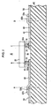
- the pcb assembly 10 comprises an electrical module 20 and a support member (circuit board, substrate) 40 having an insulative top surface 42 on which are printed firmly adherent conductors 50 and controllably adherent conductors 60.
- the electrical module 20 comprises an integrated circuit formed in a silicon chip of the flip chip or surface mount type, suitably covered by an insulating material (not shown) and having a plurality of external contacts 30 (for example, silver bumps) on a lower surface 34 thereof.
- the electrical module 20 may take various other forms as previously mentioned. It is to be noted that for illustrative purposes only, one electrical module 20 is shown. Typically, a printed circuit board assembly 10 contains a plurality of electrical modules 20 of different types.
- Support member 40 is of a suitable insulating material, such as alumina (Al2O3).
- the conductive pattern formed by the conductors 50 and 60 and the electrical module 20 form an electrical circuit of the printed circuit board assembly 10.
- the firmly adherent conductors 50 may be conventional. They are typically formed by depositing a patterned layer of a suitable ink or paste that, after firing, provides a firmly adherent conductive pattern that is compatible for use with a pattern of controllably adherent conductors 60.
- a firmly adherent conductor 50 may include copper, nickel, silver, palladium, platinum and gold and/or alloys thereof and/or other suitable metals and/or compounds to make it conductive.
- the electrical module 20 is secured to the firmly adherent conductors 50 by way of the controllably adherent conductors 60.
- Each external contact 30 of electrical module 20 is typically connected to one end 60a of a controllably adherent conductor 60 by means of a bond, such as a solder joint 32.
- the bond could be formed in various other ways, including use of a conductive adhesive epoxy or other conductive adhesive material, or the bond could be a weld.
- the other end 60b of the controllably adherent conductor 60 is bonded or fused in any suitable fashion to a contact portion 50a, typically formed by an end of a firmly adherent conductor 50.
- Firmly adherent conductors 50 are then deposited on the support member 40. This is done in conventional fashion and generally involves first screen printing a suitably patterned layer and then drying and firing the layer.
- the layer as printed is of an ink or paste that will form a firmly adhering conductive layer.
- the layer deposited is of a material commercially available from Dupont Electronics and known as Dupont 9161. It basically comprises conductive copper particles, adhesion promoters and a screening agent. Suitable other materials are available from other sources.
- the drying and firing is done in the manner prescribed by the supplier to sinter the copper particles together into a conductive layer which firmly adheres to the support member 40.
- controllably adherent conductors 60 are similarly formed by screen printing, drying and firing a layer of suitable composition.
- a second composition which is also found particularly useful, differs only in the composition of the binder, which now consists essentially of equal parts by weight of bismuth oxide and cuprous oxide, milled together.
- the cuprous oxide appears to serve primarily to promote adhesion.
- This frit can be also viewed as a mixture of bismuth oxide (0-70 percent) and the remainder a frit of the following composition by weight, 50-65 percent PbO, 5-15 percent PbF2, 20-30 percent SiO2, 0-5 percent Al2O3, and 5-15 percent B2O3 with a typical composition of this frit being by weight 55.4 percent PbO, 9.4 percent PbF2, 23.5 percent SiO2, 2.1 percent Al2O3 and 9.6 percent B2O3.
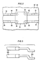
- FIG. 2 there is shown a top view of a portion of pcb assembly 10 which shows the controllably adherent conductors 60 as straight.
- Controllably adherent conductors 603 which have an S-shaped bend to reduce stress at the joint between a controllably adherent conductor 603 and a firmly adherent conductor 503.
- Conductors 503 and 603 are the same kind of conductors as conductors 50 and 60, of Figure 1 except for the bend in each controllably adherent conductor 603.
- Pcb assembly 105 is similar to pcb assembly 10 in Figure 1 and all corresponding parts thereof have the same reference number with a "5" added thereafter.
- Pcb assembly 105 is also similar to pcb assembly 104 of Figure 4 except that controllably adherent conductors 605 are S-shaped and are connected to firmly adherent conductors 505 which are connected to bonding (contact) pads 525. An electrical module to which controllably adherent conductors 605 are connected is not shown.
- Pcb assembly 107 is very similar to pcb assembly 10 of Figure 1 and to pcb assembly 104 of Figure 4 except the corresponding parts thereof have a "7" added to the last digit of the reference number.
- the rotation of the electrical module (chip) (not shown) to accommodate movement in the positions of its external contacts (not shown) and the solder joints (not shown).
- the length of the pairs of controllably adherent conductors 607 are chosen so that over a preselected operating temperature range, the changes in position of their first ends are such as to compensate for the changes in position of the external contacts (not shown).
- stresses on the solder joints are significantly limited and the reliability of pcb assembly 107 is significantly increased.
- a passage 92 (shown in dashed lines) can be formed through support member 409 and a conductor 94 can be passed therethrough to an opposite surface 96 of support member 409.
- a firmly adherent conductor 98 (shown in dashed lines) is attached to one end of conductor 94 which has a second end attached to bonding pad 529.
- support member 409 can be used as a double (two) sided printed circuit board.
- a central portion of support member 409, the portion shown as having centrally located contact 90, could have centrally located contact 90 deleted and could be instead adhesively attached to the top surface 429 by a heat conducting and electrically non-conducting epoxy or other material or compound (all not shown) to help conduct heat away from electrical module 209.
- Pcb assembly 1011 is essentially the same as pcb assembly 10 of Figure 1 except that it comprises a second electrical module 20a that is attached (soldered) via external contacts (for example, silver bumps) 30a by soldered joints 32a to portions 50b of firmly adherent conductors 50.
- Such attachment is typically used when electrical module 20a is sufficiently heavy such that if it were attached to controllably adherent conductors 60 it could endanger the integrity of the controllably adherent conductors 60 and cause them to crack and/or break.
- the electrical module 2014 has external contacts 31 thereof (which are attached to a lower surface 33 thereof) bonded, typically by solder joints 35 to (firmly adherent) portions 1014b of conductors 1014. Electrical module 2014 is typically attached to (firmly adherent) portions 1014b of conductors 1014 because in some cases it is sufficiently heavy such that if attached to portions 1014a it could endanger the integrity of portions 1014b of conductors 1014 and cause same to crack and/or break.
- the electrical module 2012 comprises an integrated circuit formed in a silicon chip of the flip chip or surface mount type, suitably covered by an insulating material (not shown) and having a plurality of external contacts 3012 (for example, silver bumps) on the lower surface 3412 thereof. These external contacts 3012 are connected to electrodes (not shown) of various circuit elements (not shown) of the electrical module 2012.
- the electrical module 2012 may take various other forms as previously mentioned. It is to be noted that for illustrative purposes only one electrical module 2012 is shown. Typically a printed circuit board assembly 1012 contains a plurality of electrical modules 2012 and 2014 of different types. It may, however, contain just one or more of electrical modules 2012.
- Each external contact 3012 of electrical module 2012 is typically connected to one part of a portion 1014a of a conductor 1014 by means of a bond, such as a solder joint 3212. All of the solder joints 3212 and 35 between both electrical modules 2012 and 2014 and the conductors 1014 could be formed in various other ways, including use of a conductive adhesive epoxy or other conductive adhesive material, or could be welds.
- the various materials involved are chosen such that mechanical stresses on the solder joints 3212 are significantly relieved by the ability of the solder joints 3212 to move relative to the support member 4012.
- the relative motion can be achieved in two basic fashions.
- the portions of the inhibitor layer 1016 under portions 1014a of conductors 1014 remain in place intimately bonded to the support member 4012 while the portions 1014a of the conductors 1014 are free to move along or lift off the inhibitor layer 1016.
- a third approach is to form the inhibitor layer by a composition that consists essentially of a finely divided refractory material (for example, alumina) suspended in an organic medium.
- a finely divided refractory material for example, alumina
- a fourth and presently preferred approach is to form the inhibitor layer by a composition that has a finely divided refractory material and a glass frit suspended in an organic medium.
- the glass frit is chosen to soften and wet both the surface of the circuit board and the refractory material, typically alumina, at a temperature below the firing temperatures. This promotes bonding among the refractory particles and between the refractory particles and the surface of the circuit board.
- the refractory material preferably an oxide such as alumina, should have negligible reaction with the conductive layer to be deposited over the inhibitor layer.
- compositions for use in printing the inhibitor layer 1016 included by weight: about 50 percent screening agent, 17 percent glass frit, and 33 percent alumina; and about 40 percent screening agent, about 20 percent glass frit and about 40 percent alumina.
- the screening agent used comprised by weight about 25 percent of a resin, typically Elvacite 2046, a product of E. I. Dupont de Nemours Inc. dissolved in a solvent, such as TEXANOL TM , a product that has been previously described, and the glass frit used comprised by weight between 60-75 percent PbO, 10-25 percent SiO2, 5-30 percent B2O3 and 0-10 percent Al2O3.
- a resin typically Elvacite 2046, a product of E. I. Dupont de Nemours Inc. dissolved in a solvent, such as TEXANOL TM , a product that has been previously described
- the glass frit used comprised by weight between 60-75 percent PbO, 10-25 percent SiO2, 5-30 percent B2O3 and 0-10 percent Al2O3.
- a solvent such as TEXANOL TM
- the glass frit used comprised by weight between 60-75 percent PbO, 10-25 percent SiO2, 5-30 percent B2O3
Landscapes
- Engineering & Computer Science (AREA)
- Microelectronics & Electronic Packaging (AREA)
- Physics & Mathematics (AREA)
- Condensed Matter Physics & Semiconductors (AREA)
- General Physics & Mathematics (AREA)
- Computer Hardware Design (AREA)
- Power Engineering (AREA)
- Manufacturing & Machinery (AREA)
- Geometry (AREA)
- Ceramic Engineering (AREA)
- Parts Printed On Printed Circuit Boards (AREA)
- Combinations Of Printed Boards (AREA)
- Coupling Device And Connection With Printed Circuit (AREA)
- Manufacturing Of Printed Wiring (AREA)
- Wire Bonding (AREA)
- Structures For Mounting Electric Components On Printed Circuit Boards (AREA)
Abstract
Description
- This invention relates to compositions of matter that are useful in forming conductive patterns on an insulating substrate or support member, techniques for forming such patterns, and assemblies using such a substrate. One such substrate is a circuit board having conductors which connect an electrical module to the circuit board to form a printed circuit board assembly.
- As used herein, the term "electrical module" is intended to include any component, such as a semiconductor chip, a light emitting or detecting device, an emitting or detecting device of magnetic nature, a magnetic storage device, a capacitor, an inductor, a resistor, a crystal, a coil, a varactor, a thermistor, a resonator, transformers, and/or a connector that may be connected in an electrical circuit, an electro-optical circuit, an optical configuration, an electro-magnetic circuit and/or a magnetic configuration. The term "printed circuit board" is intended to encompass a support member that may be rigid or flexible, laminated or not, of any suitable composition, and that includes an electrically insulative surface on which a printed pattern of electrical conductors is provided. The term "printed pattern" is intended to encompass a pattern on a substrate formed by any suitable process, including, but not limited to, silk screen printing, photolithography, evaporation, plating, stenciling, ink writing, plasma deposition, sputtering, adhesives, or thin film or thick film techniques.
- A printed circuit board having a semiconductor chip or other electrical module attached thereto shall be denoted as a printed circuit board assembly. It will be convenient to generally discuss the invention with particular reference to a printed circuit board assembly including a semiconductor chip of the surface mount or flip-chip type.
- Such a chip typically has formed thereon an integrated circuit containing a number of electrical contacts (terminals) on one surface. The contacts are typically soldered or otherwise electrically connected to the conductors of the printed circuit board.
- In the past, much effort has been focused on the use of conductors that are firmly adherent to the printed circuit board to minimize possible separation during use. Additionally, effort has also focused on maintaining the integrity of the conductor-chip interface to prevent failure at that connection. This arrangement usually operates satisfactorily. However, there are hostile environments, usually of high temperature and thermal excursions, where, during use, severe stresses cause the chip to separate from the printed circuit at or near the points of connections, that is, the solder joints. Such stresses can occur, for example, when the printed circuit board is used in an automobile.
- It is desirable to have conductors of compositions which result in a printed circuit board assembly in which the electrical modules remain reliably connected to the printed conductors in hostile environments.
- A printed circuit board assembly in accordance with the present invention is characterised by the features specified in the characterising portion of claim 1.
- The present invention solves the foregoing problems by providing on a printed circuit board a printed pattern of controllably adherent conductors. The term "controllably adherent conductor" is used to describe a conductor which adheres to the circuit board during the manufacturing process, but which is free when being used to move (slide) along and/or lift off from the circuit board in response to stresses that may arise, for example, from thermal effects, to relieve such stresses.
- This represents an approach that is the antithesis of the conventional approach mentioned above that has focused on maintaining the conductors firmly adherent to the circuit board. However, this approach does require a conductive layer for use as the controllably adherent conductor that has a degree of cohesive strength so that it does not fracture or become mechanically weak or electrically defective when separated from the circuit board.
- Typically, the printed circuit board also includes a pattern of firmly adherent conductors to which first ends of the controllably adherent conductors are connected. Second ends of the controllably adherent conductors are typically soldered to an electrical module, such as a silicon integrated circuit chip having metallic external contacts (bumps) extending from a surface thereof.
- The controllably adherent conductors and the electrical module can move to relieve stresses. This significantly reduces the possibility of breaking the bonds (typically solder joints) between the electrical module and the controllably adherent conductors. Accordingly, the reliability of the connections to the chip is improved.
- Moreover, it is feasible to use a pattern of controllably adherent conductors alone where the pulling away of the conductors occurs only in high stress areas needing stress relief. In this case the firmly adherent conductors simply define bonding or contact pads.
- In some instances a controllably adherent conductor may itself also serve as an electrical module. One example of such is a film resistor.
- Controllably adherent conductors may be provided in various arrays and configurations, some of which are described below.
- The controllably adherent conductors typically are prepared from a paste or ink which includes finely divided metal particles for conductivity and a binder. The latter is chosen to render the conductor adherent to a support member (substrate, circuit board) during processing, but to allow it to become detached from the substrate when subjected to stress during use.
- Viewed in a broader aspect, the invention is directed to an assembly that includes a support member on which are supported controllably adherent conductors that include portions thereof which are free to move on and/or lift off the support member to relieve stresses on the conductors.
- The present invention also provides specific techniques useful for forming such controllably adherent conductors. In particular, it involves the use of a localized layer, to be termed an inhibitor layer, intermediate between a circuit board and a portion of a conductive layer to achieve controlled adhesion for such portion of the conductive layer. Such controlled adhesion describes the property of a conductive layer overlying such inhibitor layer to lift off or slide along the printed circuit board in response to appropriate mechanical stress without fracture. Moreover, it includes both the situation where the inhibitor layer remains bonded to the circuit board and separates from the overlying conductive layer and the situation where the inhibitor layer remains bonded to the conductive layer and together they separate from the circuit board.
- The localized use of an inhibitor layer allows one conductive layer to have one portion used as a firmly adherent conductor by placing it in direct contact with the circuit board and to have another portion used as a controllably adherent conductor by having it overlie an inhibitor layer.
- The inhibitor layer is formed preferably by printing and subsequently firing a composition comprising essentially a mixture of a finely divided refractory material (for example, alumina or aluminium nitride) and a glass frit, suspended in an organic vehicle.
- The glass frit is chosen to soften and wet both the surface of the circuit board and the refractory material at a temperature below the firing temperatures. This promotes bonding among the refractory particles and between the refractory particles and the surface of the circuit board. The refractory material chosen should have negligible chemical reaction with the conductor.
- The present invention will now be described, by way of example, with reference to the following more detailed description taken in conjunction with the accompanying drawings, in which:-
- Figure 1 is a cross-sectional view of a portion of a printed circuit board assembly in accordance with an embodiment of the present invention;
- Figure 2 is a top view of a portion of the printed circuit board assembly shown in Figure 1;
- Figure 3 is a top view of a modification of controllably adherent conductors of the printed circuit board assembly of Figure 1;
- Figure 4 is a top view of another printed circuit board assembly in accordance with another embodiment of the present invention;
- Figure 5 is a top view of another printed circuit board assembly in accordance with a further embodiment of the present invention;
- Figure 6 is a top view of another printed circuit board assembly in accordance with a further embodiment of the present invention;
- Figure 7 is a top view of another printed circuit board assembly in accordance with a further embodiment of the present invention;
- Figure 8 is a flow chart of a typical process used to form the assemblies shown in Figures 1, 4, 5, 6, 7 and 9;
- Figure 9 is a cross-sectional view of a portion of another printed circuit board in accordance with a further embodiment of the present invention;
- Figure 10 is a graphical plot of the parameters of a furnace useful in forming the conductors on the printed circuit board assemblies of the above described figures;
- Figure 11 is a cross-sectional view of a portion of another printed circuit board assembly in accordance with a further embodiment of the present invention; and
- Figure 12 is a cross-sectional view of a portion of a printed circuit board assembly in accordance with a further embodiment of the present invention.
- It is to be noted that the drawings are not to scale. Some background lines are not shown and some figures omit cross hatching to make the drawings easier to understand.
- Referring now to Figure 1, there is shown a cross-sectional view of a portion of a printed circuit board (pcb)
assembly 10 in accordance with an embodiment of the present invention. Thepcb assembly 10 comprises anelectrical module 20 and a support member (circuit board, substrate) 40 having aninsulative top surface 42 on which are printed firmlyadherent conductors 50 and controllablyadherent conductors 60. In a typical embodiment, theelectrical module 20 comprises an integrated circuit formed in a silicon chip of the flip chip or surface mount type, suitably covered by an insulating material (not shown) and having a plurality of external contacts 30 (for example, silver bumps) on alower surface 34 thereof. Theseexternal contacts 30 are connected to electrodes (not shown) of various circuit elements (not shown) of theelectrical module 20. Theelectrical module 20 may take various other forms as previously mentioned. It is to be noted that for illustrative purposes only, oneelectrical module 20 is shown. Typically, a printedcircuit board assembly 10 contains a plurality ofelectrical modules 20 of different types. -
Support member 40 is of a suitable insulating material, such as alumina (Al₂O₃). The conductive pattern formed by theconductors electrical module 20 form an electrical circuit of the printedcircuit board assembly 10. The firmlyadherent conductors 50 may be conventional. They are typically formed by depositing a patterned layer of a suitable ink or paste that, after firing, provides a firmly adherent conductive pattern that is compatible for use with a pattern of controllablyadherent conductors 60. Such a firmlyadherent conductor 50 may include copper, nickel, silver, palladium, platinum and gold and/or alloys thereof and/or other suitable metals and/or compounds to make it conductive. - The
electrical module 20 is secured to the firmlyadherent conductors 50 by way of the controllablyadherent conductors 60. Eachexternal contact 30 ofelectrical module 20 is typically connected to oneend 60a of a controllablyadherent conductor 60 by means of a bond, such as asolder joint 32. The nature of these controllablyadherent conductors 60 will be discussed more fully below. The bond could be formed in various other ways, including use of a conductive adhesive epoxy or other conductive adhesive material, or the bond could be a weld. Theother end 60b of the controllablyadherent conductor 60 is bonded or fused in any suitable fashion to acontact portion 50a, typically formed by an end of a firmlyadherent conductor 50. All but theother end 60b of each controllablyadherent conductor 60 is controllably adherent to thetop surface 42 so that it can flex and lift off thetop surface 42 to relieve stresses on solder joints 32. Moreover, because theexternal contacts 30 of theelectrical module 20 are bound only to theends 60a of controllablyadherent conductors 60, and theelectrical module 20 is not itself bonded totop surface 42, theelectrical module 20 can also move along or lift off thetop surface 42 of thesupport member 40 to help relieve stresses at the solder joints 32. As a result, pulling apart forces are significantly reduced at eachsolder joint 32. The stresses that occur may produce either tensile or compressive stresses that are substantially completely absorbed due to the flexible nature in whichelectrical module 20 is mounted to provide a substantially stress-free and fatigue-free arrangement. - Moreover, as will be discussed more fully later, because the controllably
adherent conductors 60 are free to move, it is feasible to design the lengths of the controllablyadherent conductors 60 so that their changes in length relative to the changes in the lengths of the relevant portion of the (alumina)support member 40 and of theelectrical module 20 balance over an operating temperature range to further relieve stresses in the solder joints 32. - Referring now to Figure 8, there is shown a flow chart of a typical process for preparing the
pcb assembly 10 shown in Figure 1. As indicated, a ceramic printed circuit board, typically of alumina, is used as the support member ofsubstrate 40. - Firmly
adherent conductors 50 are then deposited on thesupport member 40. This is done in conventional fashion and generally involves first screen printing a suitably patterned layer and then drying and firing the layer. The layer as printed, is of an ink or paste that will form a firmly adhering conductive layer. In a preferred embodiment, the layer deposited is of a material commercially available from Dupont Electronics and known as Dupont 9161. It basically comprises conductive copper particles, adhesion promoters and a screening agent. Suitable other materials are available from other sources. After printing, the drying and firing is done in the manner prescribed by the supplier to sinter the copper particles together into a conductive layer which firmly adheres to thesupport member 40. - Referring now to Figure 10, there is shown a graphical plot of the parameters of a furnace (not shown) that can be used for the firing process. In the plot, the y axis shows temperature in degrees C of successive zones of the furnace and the x axis shows elapsed time in minutes as a workpiece (for example, a
support member 40 with ink patterns which will becomeconductors 50 and/or 60) moves along a belt (not shown) through the various temperature zones existing within the furnace. The terms "ENTRANCE" and "EXIT" shown in Figure 10 indicate the workpiece entering and exiting, respectively, the furnace. As is seen, the workpiece takes slightly more than twenty minutes to reach the maximum temperature of about 900°C during which time the organic vehicle in the original paste or ink is being removed. It then takes about ten minutes to pass through the furnace zone at this peak temperature during which the copper particles are sintered into a conductive layer. Finally, it is allowed to cool gradually to room temperature over about a twenty minute period to reduce thermal shock. Of course, the optimum parameters are usually a function of the particular paste or ink being used. - Next, the controllably
adherent conductors 60 are similarly formed by screen printing, drying and firing a layer of suitable composition. - To avoid the need for separate furnaces, it is advantageous to choose compositions for use in forming both the firmly
adherent conductors 50 and the controllablyadherent conductors 60 that can be processed in the same way. When this is done, the drying and firing of the composition used to form controllablyadherent conductors 60 are carried out in the same manner as described previously for the firmlyadherent conductors 50 as discussed with reference to Figure 10. The controllablyadherent conductors 60 are formed to extend between the firmlyadherent conductors 50 and where theexternal contacts 30 of theelectrical modules 20 are to be positioned. - Special compositions are used to form controllably
adherent conductors 60 to provide the desired controllable adherent properties and to be compatible for use with firmlyadherent conductors 50. - Several compositions are presently of particular interest for use to form controllably
adherent conductors 60 of the kind described. These compositions have the advantage that they have the desired compatibility with firmlyadherent conductors 50. - The first composition, which is preferred for some applications, includes by weight about 88.5 percent of a conductor, about 10 percent of a suitable screening agent, and about 1.5 percent of a binder. The conductor is finely divided copper powder with an average particle size of between 1 and 2 microns. The specific screening agent is a mixture of about 90 percent by weight of a solvent, typically TEXANOLTM (believed to be 2,2,4 Trimethyl 1,3 Pentanedio Monoisobutyrate), and the remainder of a resin, typically ethyl cellulose grade N-50, both of which are available commercially. The binder consists essentially of bismuth oxide (Bi₂O₃) which serves to promote both adhesion of the layer of controllably
adherent conductor 60 to thesupport member 40 during processing and cohesion of the copper particles after firing. - Too large an amount of the binder undesirably increases adhesion to the
support member 40 and makes it difficult for the controllablyadherent conductors 60 to lift off thetop surface 42 of thesupport member 40 to accommodate mechanical stresses. Too little of the binder results in nonadherence immediately after firing, preventing any subsequent processing. Typically, the binder should be at least 0.05 percent and no more than 5.0 percent of the composition, although if the binder is chosen to be one largely lost during firing, or is not a very effective adhesion promoter, larger amounts initially may be feasible. The appropriate limits can be expected to be dependent on the characteristics of the metal powder employed. - The screening agent should be chosen to facilitate the screen printing, and various other agents should be suitable. Moreover, the fraction of the solvent in the screening agent typically is between 85 and 98 percent.
- A second composition, which is also found particularly useful, differs only in the composition of the binder, which now consists essentially of equal parts by weight of bismuth oxide and cuprous oxide, milled together. Here the cuprous oxide appears to serve primarily to promote adhesion.
- Another composition that proved useful included by weight about 89 percent powdered copper, about one percent of a frit as the binder, and about 10 percent of the screening agent described above in which the frit included by weight about 70.0 percent bismuth oxide (Bi₂O₃), 15.6 percent lead oxide (PbO), 4.5 percent lead fluoride (PbF₂), 6.6 percent silicon dioxide (SiO₂), 0.6 percent aluminum oxide (Al₂O₃), and 2.7 percent boron oxide (B₂O₃).
- The components of this frit by weight could be varied with the Bi₂O₃ between 0-73 percent, the PbO between 15-60 percent, the PbF₂ between 4-12 percent, the SiO₂ between 5-25 percent and the Al₂O₃ between 0.5-2.5 percent and the B₂O₃ between 2-10 percent. This frit can be also viewed as a mixture of bismuth oxide (0-70 percent) and the remainder a frit of the following composition by weight, 50-65 percent PbO, 5-15 percent PbF₂, 20-30 percent SiO₂, 0-5 percent Al₂O₃, and 5-15 percent B₂O₃ with a typical composition of this frit being by weight 55.4 percent PbO, 9.4 percent PbF₂, 23.5 percent SiO₂, 2.1 percent Al₂O₃ and 9.6 percent B₂O₃.
- Two other compositions that proved successful included by weight 89.25 and 89.5 percent copper powder, respectively, 10 percent of the screening agent described earlier and the balance a frit that included by weight 60-75 percent PbO, 10-25 percent SiO₂, 5-30 percent B₂O₃ and 0-10 percent Al₂O₃. One embodiment which proved successful included a glass frit approximately by weight 66.6 percent PbO, 22.4 percent SiO₂, 8.7 percent B₂O₃ and 2.3 percent Al₂O₃.
- These examples demonstrate the wide range of mixtures that can be used as the binder in the compositions to achieve the controllably
adherent conductor 60 needed. - In general, the compositions especially useful for forming controllably
adherent conductors 60 comprise between 75 and 92 percent finely divided copper powder, with an average particle size of between about 0.5 and 5.0 microns, 7.5 to 20 percent of a screening agent, and the remainder essentially of a binder to promote adequate cohesion and controllable adhesion of the kind described. In a preferred range, the copper has an average particle size between 1 and 2 microns and comprises between 85 and 90 percent of the mixture. - A variety of other compositions should be suitable including some that use other kinds of conductive particles, such as silver, palladium, nickel, platinum and gold and/or alloys thereof. Moreover, in some instances, it may prove advantageous to include a surfactant to improve wetting. The composition should result in controllably adherent conductive layers having characteristics compatible with those of the firmly adherent conductive layers.
- Next, optionally there may be printed, dried and fired other layers that serve special roles, such as thick film resistors. In some instances, in order to provide different values of thick film resistors, two or more resistive compositions are included that require separate processing. This step may be repeated as needed to deposit all such thick film resistors.
- Finally, as indicated in Figure 8, the
electrical module 20 of thepcb assembly 10 is electrically connected to the controllablyadherent conductors 60. - Typically, this first includes printing solder dots on the
ends 60a of controllablyadherent conductors 60 where such ends 60a are to be attached to theexternal contacts 30 of theelectrical module 20. This can be done in conventional fashion. Advantageously, the solder paste used to form the solder dots comprises a 25/75 tin-lead solder. After the solder paste is deposited, theelectrical module 20 is appropriately positioned to have itsexternal contacts 30 aligned with the solder dots. Then thepcb assembly 10 is heated to a temperature to melt and reflow the solder and then cooled to solidify resulting solder joints 32 between theexternal contacts 30 and theends 60a of controllablyadherent conductors 60. - It should be apparent that it would be feasible, if desired, to print or form the controllably
adherent conductors 60 before printing or forming the firmlyadherent conductors 50. - In some instances, it may be feasible to use a single furnace operation to form both patterns of conductors simultaneously.
- When the
pcb assembly 10 thus prepared is placed in operation and subjected to sufficiently high stresses, these stresses are absorbed by the controllablyadherent conductors 60, which lose their adhesion to thesupport member 40 and then are free to move along and/or lift off thetop surface 42 of thesubject matter 40. - In an embodiment of
pcb assembly 10 in accordance with the invention: theexternal contacts 30 ofelectrical module 20 are made of silver and each has a height in the range of 0.018 to 0.076 mm (0.0007 to 0.003 inches) and a diameter of about 0.153 mm (0.006 inches); theelectrical module 20 is square in shape and has dimensions in the range of 4.57 to 7.62 mm (0.180 to 0.3 inches); and the solder joints 32 are formed using a 25/75 tin lead solder; each of controllablyadherent conductors 60 has a width of 0.127 to 0.254 mm (0.005 to 0.01 inches), a length of 1.02 to 3.81 mm (0.04 to 0.150 inches) and a thickness of 0.008 to 0.02 mm (0.0003 to 0.0008 inches). Various other parameters, such as the thickness of controllablyadherent conductors 60 in the range of 0.008 to 0.025 mm (0.0003 to 0.001 inches), are, of course, feasible. - The dimensions of the controllably
adherent conductors 60 advantageously are designed to provide optimal performance of their function with a minimal amount of conductor material. Various conductor configurations are feasible and typical configurations are described below. - Referring again to Figure 1, in one presently preferred design, the thermal expansion rate (change in length/unit change in temperature) of dimension A to D along the controllably
adherent conductors 60 and the electrical module (chip) 20 is equal to that of the dimension of E to F along thesupport member 40. The rate of expansion is determined by the thermal expansion coefficient of the type of material and the length of material that is of concern. Thus, if the rate of expansion of distance A to B, B to C and C to D are added, they become that of A to D, which should be equal to the rate of expansion of E to F. For a givenpcb assembly 10, the dimension B to C is fixed by theelectrical module 20 design. However, the dimensions A to B and C to D can be made of any desirable length. By adjusting the length of A to B and C to D (normally these would be equal), the sums of the rates of all three components can be made equal to that of E to F. Onepcb assembly 10, which was built on an alumina substrate (support member 40), had a length (A to B) = (C to D) = 11.18 mm (0.44 inches) and used anelectrical module 20 having a square dimension of 7.21 mm (0.284 inches) (B to C). - The controllably adherent conductors may be formed in various shapes as desired, since the shape, while important, is not critical.
- Referring now to Figure 2, there is shown a top view of a portion of
pcb assembly 10 which shows the controllablyadherent conductors 60 as straight. - Referring now to Figure 3, there is shown a top view of controllably
adherent conductors 603 which have an S-shaped bend to reduce stress at the joint between a controllablyadherent conductor 603 and a firmlyadherent conductor 503.Conductors conductors adherent conductor 603. - Referring now to Figure 4, there is shown a top view of a printed circuit board (pcb)
assembly 104.Pcb assembly 104 is similar topcb assembly 10 of Figure 1, and all corresponding parts thereof have the same reference number with a "4" added thereafter. One end of each of firmlyadherent conductors 504 mechanically and electrically contacts a bonding (contact)pad 52 which firmly adheres totop surface 424 ofsupport member 404. Controllablyadherent conductors 604 are straight. Each of controllablyadherent conductors 604 is shown having two parallel fingers. This configuration is useful for testing, but asingle finger conductor 604 is typically preferable. It is to be noted that the firmlyadherent conductors 504 can be eliminated with controllablyadherent conductors 604 then being connected directly tobonding pads 52. Still further,bonding pads 52 can be modified in shape and size and brought out to an edge ofsupport member 404 to serve as the male portion of a connector assembly (not shown) that is adapted to plug into a female portion (not shown) of the connector assembly. - Referring now to Figure 5, there is shown a top view of a printed
circuit board assembly 105.Pcb assembly 105 is similar topcb assembly 10 in Figure 1 and all corresponding parts thereof have the same reference number with a "5" added thereafter.Pcb assembly 105 is also similar topcb assembly 104 of Figure 4 except that controllablyadherent conductors 605 are S-shaped and are connected to firmlyadherent conductors 505 which are connected to bonding (contact)pads 525. An electrical module to which controllablyadherent conductors 605 are connected is not shown. - Referring now to Figure 6, there is shown a top view of a printed
circuit board assembly 106.Pcb assembly 106 is similar topcb assembly 10 of Figure 1 and all corresponding parts thereof have the same reference number with a "6" added thereafter.Pcb assembly 106 is also similar topcb assembly 105 of Figure 5 except that the controllablyadherent conductors 606 are angled with respect to the electrical module (chip) (not shown) they contact. Printedcircuit board assembly 106 allows the chip to rotate so as to relieve stress where the chip is soldered to controllablyadherent conductors 606. - Referring now to Figure 7, there is shown a top view of a printed
circuit assembly 107.Pcb assembly 107 is very similar topcb assembly 10 of Figure 1 and topcb assembly 104 of Figure 4 except the corresponding parts thereof have a "7" added to the last digit of the reference number. In this case, there is no provision for the rotation of the electrical module (chip) (not shown) to accommodate movement in the positions of its external contacts (not shown) and the solder joints (not shown). Instead, the length of the pairs of controllablyadherent conductors 607 are chosen so that over a preselected operating temperature range, the changes in position of their first ends are such as to compensate for the changes in position of the external contacts (not shown). As a result, stresses on the solder joints are significantly limited and the reliability ofpcb assembly 107 is significantly increased. - It should be apparent that the invention is largely independent of the specific nature of the electrical module connected into the printed circuit. It could be simply any circuit component as listed above that has contacts on one surface by which the circuit component is to be connected. It may also be a connector whose various pins are to be connected to ends of the controllably adherent conductors.
- Additionally, as was mentioned earlier, the term "printed circuit board" can encompass a wide variety of forms since the nature of the substrate on which the controllably adherent conductors are deposited need only be compatible with the desired controllable adhesion of the conductive layer deposited.
- In particular, the substrate or support member may even be a semiconductor wafer on which are deposited controllably adherent conductors for connecting components therein. Additionally, the substrate or support member may be a first semiconductor chip on top of which is connected a second semiconductor chip by way of controllably adherent conductors which are free to move on and/or away from a surface of the first chip.
- Moreover, the invention may be feasible with superconductive circuits in which either the controllably adherent or firmly adherent conductors are superconductors.
- Similarly, it should be apparent that the specific nature of the circuit board that serves as the substrate or support member is not critical. In particular, the circuit board need not be rigid but may be of a flexible kind. Also, it need not be ceramic but may be of any suitable composition that is compatible with controlled adhesion.
- In some instances, it may prove desirable to provide a resilient coating over the surface of the electrical module including its contacts, to cushion any movement of the electrical module. In other instances, particularly when an electrical module is of relatively large mass, it may be desirable to restrain its movement.
- Referring now to Figure 9, there is shown a cross-sectional view of a portion of a printed
circuit board assembly 109 that is very similar topcb assembly 10 of Figure 1 and the corresponding parts thereof have a "9" added to the last digit of the reference number.Pcb assembly 109 has anelectrical module 209 which has a plurality of external contacts (bumps) 309 and has an essentially centrally located contact (bump) 90 which is soldered via a solder joint 329 to a firmly adherent conductive contact region (bonding pad 529) on thetop surface 429 of the support member 409. This results in the centre portion ofelectrical module 209 being essentially fixed to thetop surface 429 of support member 409. Portions ofelectrical module 209 other than the centre portion thereof are free to move to relieve stress as are controllablyadherent conductors 609. - A passage 92 (shown in dashed lines) can be formed through support member 409 and a
conductor 94 can be passed therethrough to anopposite surface 96 of support member 409. A firmly adherent conductor 98 (shown in dashed lines) is attached to one end ofconductor 94 which has a second end attached tobonding pad 529. Thus support member 409 can be used as a double (two) sided printed circuit board. A central portion of support member 409, the portion shown as having centrally locatedcontact 90, could have centrally locatedcontact 90 deleted and could be instead adhesively attached to thetop surface 429 by a heat conducting and electrically non-conducting epoxy or other material or compound (all not shown) to help conduct heat away fromelectrical module 209. This added heat dissipation mechanism allows for the use of larger chips with associated higher power dissipation than might be otherwise possible. In some instances the epoxy could be electrically conductive and could be used to bring electrical signals and/or power to theelectrical module 209. A plurality of contacts, each like centrally locatedcontact 90, could be substituted for centrally locatedcontact 90. These substituted contacts would be attached to central portions ofelectrical module 209 and would serve to enhance the mechanical integrity ofpcb assembly 109 during vibration of same. The substituted contacts could also serve to bring electrical signals and/or power toelectrical module 209. - It should also be apparent that the printed circuit board may support one or more electrical modules with some free to move on the circuit board in the manner discussed and with others that are fixed in place in conventional fashion.
- Referring now to Figure 11, there is a cross sectional view of a portion of a printed
circuit board assembly 1011.Pcb assembly 1011 is essentially the same aspcb assembly 10 of Figure 1 except that it comprises a secondelectrical module 20a that is attached (soldered) via external contacts (for example, silver bumps) 30a bysoldered joints 32a toportions 50b of firmlyadherent conductors 50. Such attachment is typically used whenelectrical module 20a is sufficiently heavy such that if it were attached to controllablyadherent conductors 60 it could endanger the integrity of the controllablyadherent conductors 60 and cause them to crack and/or break. The components ofpcb assembly 1011 which are very similar or identical to those ofpcb assembly 10 of Figure 1 have the same reference number.Electrical modules 20a advantageously are fabricated from materials which have a coefficient of thermal expansion which is close to that ofsupport member 40 and therefore solderjoints 30a will experience little stress as a result of thermal changes. Typically, thick or thin film resistors printed on a circuit board would be connected to firmlyadherent conductors 50 as would a chip that is to be wire bonded to the circuit board. - If one composition is used to form all conductors, differences in adhesion to the circuit board can be achieved by modifying portions of substrate on a microscopic scale to alter adhesion whereas other portions of the circuit board are left in the normal state. Another technique which uses one composition to form both firmly adherent and controllably adherent conductors on a common circuit board is described below.
- Referring now to Figure 12, there is shown a cross sectional view of a portion of a printed
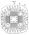
circuit board assembly 1012 in accordance with a further embodiment of the present invention. Thepcb assembly 1012 compriseselectrical modules top surface 4212 on which are printed (formed)conductors 1014 havingportions 1014a which are separated fromtop surface 4212 by aninhibitor layer 1016 and havingportions 1014b which make direct contact withtop surface 4212. Theportions 1014a ofconductors 1014 where theinhibitor layer 1016 lies intermediate betweentop surface 4212 and theconductors 1014 are controllably adherent. Theportions 1014b ofconductors 1014 where theconductor 1014 is in intimate contact with thetop surface 4212 are firmly adherent. - The
electrical module 2012 hasexternal contacts 3012 thereof (which are attached to abottom surface 3412 of module 2012) bonded, typically bysolder joints 3212, to theportions 1014a ofconductors 1014. As a result, theportions 1014a ofconductors 1014 are controllably adherent and are able to move along and/or lift offtop surface 4212 of thesupport member 4012 as needed to relieve mechanical stresses on the solder joints 3212. - The
electrical module 2014 has external contacts 31 thereof (which are attached to alower surface 33 thereof) bonded, typically by solder joints 35 to (firmly adherent)portions 1014b ofconductors 1014.Electrical module 2014 is typically attached to (firmly adherent)portions 1014b ofconductors 1014 because in some cases it is sufficiently heavy such that if attached toportions 1014a it could endanger the integrity ofportions 1014b ofconductors 1014 and cause same to crack and/or break. - In a typical embodiment the
electrical module 2012 comprises an integrated circuit formed in a silicon chip of the flip chip or surface mount type, suitably covered by an insulating material (not shown) and having a plurality of external contacts 3012 (for example, silver bumps) on thelower surface 3412 thereof. Theseexternal contacts 3012 are connected to electrodes (not shown) of various circuit elements (not shown) of theelectrical module 2012. Theelectrical module 2012 may take various other forms as previously mentioned. It is to be noted that for illustrative purposes only oneelectrical module 2012 is shown. Typically a printedcircuit board assembly 1012 contains a plurality ofelectrical modules electrical modules 2012. - The conductive pattern formed by the
conductors 1014 and theelectrical modules circuit board assembly 1012. Theconductors 1014 are typically formed by depositing a patterned layer of a suitable ink or paste that, after firing, provides a conductive pattern.Such conductors 1014 may include copper, nickel, silver, palladium, platinum and gold and/or alloys thereof and/or other suitable metals and/or compounds to make them conductive. - In a preferred embodiment, the conductive layer was formed by the use of Dupont 9161, previously described, which comprises essentially finely divided copper particles, a screening agent and adhesion promoters.
- Each
external contact 3012 ofelectrical module 2012 is typically connected to one part of aportion 1014a of aconductor 1014 by means of a bond, such as asolder joint 3212. All of thesolder joints 3212 and 35 between bothelectrical modules conductors 1014 could be formed in various other ways, including use of a conductive adhesive epoxy or other conductive adhesive material, or could be welds. - In accordance with the invention, the various materials involved are chosen such that mechanical stresses on the
solder joints 3212 are significantly relieved by the ability of thesolder joints 3212 to move relative to thesupport member 4012. The relative motion can be achieved in two basic fashions. - In the first, the
portions 1014a ofconductors 1014 remain intimately bonded (attached) to portions of theinhibitor layer 1016 therebelow and together they move along and/or lift offsupport member 4012. This approach has the potential of increasing the mechanical strength of the composite layer portions. - In the other approach, the portions of the
inhibitor layer 1016 underportions 1014a ofconductors 1014 remain in place intimately bonded to thesupport member 4012 while theportions 1014a of theconductors 1014 are free to move along or lift off theinhibitor layer 1016. - A conductive layer printed on a circuit board depends for its adhesion to the circuit board on a reaction between the surface of the board and the ingredients in the composition (for example, ink) used to print the conductive layer. For controlled adhesion of the kind desired, it is necessary to partially stifle this reaction so that the layer can separate from the circuit board in response to mechanical stress.
- When the ink being used to print a conductive layer includes adhesion promoters that react and insure firm adhesion where applied directly to a substrate, such as the surface of a printed circuit board, an inhibitor layer must serve to restrain such reaction.
- There are several possible approaches to providing such an inhibitor layer.
- A first approach is to use an inhibitor layer that essentially includes only an organic vehicle that has poor burn-out characteristics under the firing conditions used, such as the case where a nitrogen atmosphere is used for firing a conductive layer (for example, copper), so that little reaction is created with the substrate for promoting adhesion because excessive organics render the binders in the ink ineffective.
- A second approach involves using as the inhibitor layer a film including essentially only an organic vehicle that has excellent burn-out to lessen a chance of reaction between the adhesive promoters and the substrate. This approach is suitable in cases where no residual organics on the substrate are tolerable.
- A third approach is to form the inhibitor layer by a composition that consists essentially of a finely divided refractory material (for example, alumina) suspended in an organic medium.
- A fourth and presently preferred approach is to form the inhibitor layer by a composition that has a finely divided refractory material and a glass frit suspended in an organic medium. As mentioned earlier, the glass frit is chosen to soften and wet both the surface of the circuit board and the refractory material, typically alumina, at a temperature below the firing temperatures. This promotes bonding among the refractory particles and between the refractory particles and the surface of the circuit board. The refractory material, preferably an oxide such as alumina, should have negligible reaction with the conductive layer to be deposited over the inhibitor layer.
- In a specific embodiment of the invention in accordance with the last approach, the
inhibitor layer 1016 was formed by printing a composition comprising by weight essentially about 80 percent a screening agent, about 10 percent a glass frit and about 10 percent alumina (Al₂O₃). Moreover the glass frit consisted by weight essentially of about 66.6 percent lead oxide (PbO), 22.4 percent silicon dioxide (SiO₂), 8.7 percent boron trioxide (B₂O₃) and 2.3 percent alumina (Al₂O₃). - Other suitable compositions for use in printing the
inhibitor layer 1016 included by weight: about 50 percent screening agent, 17 percent glass frit, and 33 percent alumina; and about 40 percent screening agent, about 20 percent glass frit and about 40 percent alumina. - In these compositions the screening agent used comprised by weight about 25 percent of a resin, typically Elvacite 2046, a product of E. I. Dupont de Nemours Inc. dissolved in a solvent, such as TEXANOLTM, a product that has been previously described, and the glass frit used comprised by weight between 60-75 percent PbO, 10-25 percent SiO₂, 5-30 percent B₂O₃ and 0-10 percent Al₂O₃. Various glass frit compositions other than the specific composition described can be used consistent with the requirements mentioned above. Alternatively, certain oxides, such as bismuth oxide (Bi₂O₃), which serve essentially the same function as the glass frit, can be substituted for the glass frit. These certain oxides are denoted as "oxide binders".
- The thickness of the
inhibitor layer 1016 is desirably as thin as can be printed reliably to minimize topographical changes in theconductors 1014. The surface area of theinhibitor layer 1016 is sufficient to encompass the regions desired for controlled adhesion but need not necessarily be patterned to be congruent in width and length with the conductive layer. The thickness of theinhibitor layer 1016 is typically in the range of 0.0025 to 0.025 mm (0.0001 to 0.001 inches) with a preferred range of 0.005 to 0.013 mm (0.0002 to 0.0005 inches). Ablanket inhibitor layer 1016 could be used instead of separated inhibitor layers for eachportion 1014a of theconductors 1014 which are to be characterized by controlled adhesion. The thickness of theconductors 1014 is typically in the range of 0.0076 to 0.025 mm (0.0003 to 0.001 inches) with a preferred range of 0.01 to 0.02 mm (0.0004 to 0.0008 inches). Generally, the thickness of theinhibitor layer 1016 after firing can be controlled both by the thickness of the layer printed and the percentage of the inorganic solids (the glass frit and the refractory materials) in the composition printed. Generally, such solids should be between 5 and 85 percent by weight of the composition. The degree of adhesion is determined primarily by the ratio of the amount of glass frit and the amount of refractory materials in the composition. This ratio most advantageously is in the range between 0.1 and 2.0. - The printed patterns can be formed in two basic ways.
- The presently preferred way is first to print the composition that provides the inhibitor layer and merely to dry this layer without firing. Then there is printed and dried the composition that provides the conductive layer. The resultant is then heated for firing both layers in the same heating cycle. The heating cycle used is that recommended by the manufacturer for Dupont 9161 composition and basically is that previously discussed with reference to Figure 10.
- Alternatively, depending on the nature of the selected conductor and inhibitor, the first layer could be both dried and fired before deposition of the second layer.
- Examples of refractory oxides that can be used instead of Al₂O₃ are SiO₂, ZrO₂ and TiO₂. A combination of any of these four refractory oxides could also be used.
- As mentioned previously, other refractory materials, such as nitrides, should be useful in place of the refractory oxides if compatible with the glass frit.
- Various other compositions for both the inhibitor layer and the conductive layer can be expected to be useful, consistent with the principles set forth including particularly various other screening agents and amounts of screening agents.
- Moreover, the principles of controlled adhesion that have been discussed above in the context of electrical application to printed circuit board technology are not limited to such application. The principles can be extended to applications in which the controllably adherent conductors serve primarily mechanical rather than primarily electrical roles. The principles can be further extended to applications in which non-electrically conductive members (runners), which have essentially the same controlled adhesion as the controllably adherent conductors, are used in mechanical roles.
Claims (35)
Applications Claiming Priority (6)
| Application Number | Priority Date | Filing Date | Title |
|---|---|---|---|
| US23274388A | 1988-08-16 | 1988-08-16 | |
| US232743 | 1988-08-16 | ||
| US07/297,212 US4959751A (en) | 1988-08-16 | 1989-01-17 | Ceramic hybrid integrated circuit having surface mount device solder stress reduction |
| US07/297,201 US5122929A (en) | 1988-08-16 | 1989-01-17 | Method of achieving selective inhibition and control of adhesion in thick-film conductors |
| US297201 | 1989-01-17 | ||
| US297212 | 1989-01-17 |
Publications (3)
| Publication Number | Publication Date |
|---|---|
| EP0355965A2 true EP0355965A2 (en) | 1990-02-28 |
| EP0355965A3 EP0355965A3 (en) | 1991-08-07 |
| EP0355965B1 EP0355965B1 (en) | 1995-02-15 |
Family
ID=27398339
Family Applications (1)
| Application Number | Title | Priority Date | Filing Date |
|---|---|---|---|
| EP89306821A Expired - Lifetime EP0355965B1 (en) | 1988-08-16 | 1989-07-05 | A method of achieving selective inhibition and control of adhesion in thick-film conductors |
Country Status (4)
| Country | Link |
|---|---|
| EP (1) | EP0355965B1 (en) |
| JP (1) | JPH02106089A (en) |
| KR (1) | KR920005986B1 (en) |
| DE (1) | DE68921116T2 (en) |
Cited By (3)
| Publication number | Priority date | Publication date | Assignee | Title |
|---|---|---|---|---|
| EP0486392A1 (en) * | 1990-11-16 | 1992-05-20 | Commissariat A L'energie Atomique | Hybrid circuit formed by two circuits whose tracks are joined by electrical connection balls |
| EP0719453A1 (en) * | 1993-09-13 | 1996-07-03 | Olin Corporation | Flip chip in metal electronic packages |
| CN116514402A (en) * | 2023-05-06 | 2023-08-01 | 乾宇微纳技术(深圳)有限公司 | Glass powder applied to negative thick film photoresist paste and preparation method thereof |
Families Citing this family (2)
| Publication number | Priority date | Publication date | Assignee | Title |
|---|---|---|---|---|
| KR100475407B1 (en) * | 1996-12-30 | 2005-06-08 | 고려화학 주식회사 | Inorganic Low Temperature Curing Composition |
| DE60037069T2 (en) * | 1999-05-28 | 2008-09-11 | Denki Kagaku Kogyo K.K. | Circuit with substrate |
Citations (5)
| Publication number | Priority date | Publication date | Assignee | Title |
|---|---|---|---|---|
| FR2479639A1 (en) * | 1980-03-25 | 1981-10-02 | Thomson Csf | Electronic component mounting process for PCB - uses metal bridges in contact with metal tracks to permit substrate flexing without damage to solder joints |
| EP0044247A1 (en) * | 1980-07-11 | 1982-01-20 | Socapex | Method of producing a carrier for electronic components for the interconnection of integrated-circuit chips |
| EP0075890A2 (en) * | 1981-09-30 | 1983-04-06 | Siemens Aktiengesellschaft | Arrangement to prevent damage of the components or conductors on a circuit board |
| EP0245697A2 (en) * | 1986-05-07 | 1987-11-19 | International Business Machines Corporation | Multilayered thin film metallurgy for brazing input/output pins to a ceramic substrate |
| EP0263277A2 (en) * | 1986-10-06 | 1988-04-13 | International Business Machines Corporation | A flexible electrical connection and method of making same |
-
1989
- 1989-07-05 DE DE68921116T patent/DE68921116T2/en not_active Expired - Fee Related
- 1989-07-05 EP EP89306821A patent/EP0355965B1/en not_active Expired - Lifetime
- 1989-08-16 KR KR1019890011644A patent/KR920005986B1/en not_active IP Right Cessation
- 1989-08-16 JP JP1211193A patent/JPH02106089A/en active Pending
Patent Citations (5)
| Publication number | Priority date | Publication date | Assignee | Title |
|---|---|---|---|---|
| FR2479639A1 (en) * | 1980-03-25 | 1981-10-02 | Thomson Csf | Electronic component mounting process for PCB - uses metal bridges in contact with metal tracks to permit substrate flexing without damage to solder joints |
| EP0044247A1 (en) * | 1980-07-11 | 1982-01-20 | Socapex | Method of producing a carrier for electronic components for the interconnection of integrated-circuit chips |
| EP0075890A2 (en) * | 1981-09-30 | 1983-04-06 | Siemens Aktiengesellschaft | Arrangement to prevent damage of the components or conductors on a circuit board |
| EP0245697A2 (en) * | 1986-05-07 | 1987-11-19 | International Business Machines Corporation | Multilayered thin film metallurgy for brazing input/output pins to a ceramic substrate |
| EP0263277A2 (en) * | 1986-10-06 | 1988-04-13 | International Business Machines Corporation | A flexible electrical connection and method of making same |
Cited By (6)
| Publication number | Priority date | Publication date | Assignee | Title |
|---|---|---|---|---|
| EP0486392A1 (en) * | 1990-11-16 | 1992-05-20 | Commissariat A L'energie Atomique | Hybrid circuit formed by two circuits whose tracks are joined by electrical connection balls |
| FR2669500A1 (en) * | 1990-11-16 | 1992-05-22 | Commissariat Energie Atomique | HYBRID CIRCUIT FORMED OF TWO CIRCUITS OF WHICH THE TRACKS ARE CONNECTED BY ELECTRICAL CONNECTION BALLS. |
| US5225634A (en) * | 1990-11-16 | 1993-07-06 | Commissariat A L'energie Atomique | Hybrid circuit formed of two circuits whose tracks are connected by electric connection balls |
| EP0719453A1 (en) * | 1993-09-13 | 1996-07-03 | Olin Corporation | Flip chip in metal electronic packages |
| EP0719453A4 (en) * | 1993-09-13 | 1998-08-19 | Olin Corp | Flip chip in metal electronic packages |
| CN116514402A (en) * | 2023-05-06 | 2023-08-01 | 乾宇微纳技术(深圳)有限公司 | Glass powder applied to negative thick film photoresist paste and preparation method thereof |
Also Published As
| Publication number | Publication date |
|---|---|
| KR920005986B1 (en) | 1992-07-25 |
| EP0355965A3 (en) | 1991-08-07 |
| EP0355965B1 (en) | 1995-02-15 |
| KR900004228A (en) | 1990-03-27 |
| DE68921116D1 (en) | 1995-03-23 |
| DE68921116T2 (en) | 1995-06-08 |
| JPH02106089A (en) | 1990-04-18 |
Similar Documents
| Publication | Publication Date | Title |
|---|---|---|
| US5121298A (en) | Controlled adhesion conductor | |
| US3429040A (en) | Method of joining a component to a substrate | |
| US4612601A (en) | Heat dissipative integrated circuit chip package | |
| US5897724A (en) | Method of producing a hybrid integrated circuit | |
| EP0260490A1 (en) | Bonding sheet for electronic component and method of bonding electronic component using the same | |
| US5176853A (en) | Controlled adhesion conductor | |
| KR970010893B1 (en) | Kinetic solder paste composition | |
| EP0453858B1 (en) | Process for brazing metallized components to ceramic substrates | |
| JPH10256315A (en) | Semiconductor chip bonding pad and its formation | |
| US5122929A (en) | Method of achieving selective inhibition and control of adhesion in thick-film conductors | |
| US3495133A (en) | Circuit structure including semiconductive chip devices joined to a substrate by solder contacts | |
| JPH077038A (en) | Electronic package | |
| US4908696A (en) | Connector and semiconductor device packages employing the same | |
| US20020076910A1 (en) | High density electronic interconnection | |
| US4959751A (en) | Ceramic hybrid integrated circuit having surface mount device solder stress reduction | |
| JP2022068307A (en) | Leadless stack consisting of multiple components | |
| JP2505739B2 (en) | Housing for electronic devices | |
| US5334422A (en) | Electrical connector having energy-formed solder stops and methods of making and using the same | |
| EP0355965B1 (en) | A method of achieving selective inhibition and control of adhesion in thick-film conductors | |
| JP3336240B2 (en) | Semiconductor element mounting board | |
| EP0200469B1 (en) | Metallizing paste for silicon carbide sintered body and a semiconductor device including the same | |
| WO1997030461A1 (en) | Resistor network in ball grid array package | |
| JPH05218133A (en) | Semiconductor element mounting board and mounting method therefor | |
| JPS6332266B2 (en) | ||
| KR970004545B1 (en) | Gold conductor composition |
Legal Events
| Date | Code | Title | Description |
|---|---|---|---|
| PUAI | Public reference made under article 153(3) epc to a published international application that has entered the european phase |
Free format text: ORIGINAL CODE: 0009012 |
|
| AK | Designated contracting states |
Kind code of ref document: A2 Designated state(s): DE FR GB IT |
|
| PUAL | Search report despatched |
Free format text: ORIGINAL CODE: 0009013 |
|
| AK | Designated contracting states |
Kind code of ref document: A3 Designated state(s): DE FR GB IT |
|
| RHK1 | Main classification (correction) |
Ipc: H05K 3/40 |
|
| 17P | Request for examination filed |
Effective date: 19911001 |
|
| 17Q | First examination report despatched |
Effective date: 19930322 |
|
| ITF | It: translation for a ep patent filed | ||
| GRAA | (expected) grant |
Free format text: ORIGINAL CODE: 0009210 |
|
| AK | Designated contracting states |
Kind code of ref document: B1 Designated state(s): DE FR GB IT |
|
| REF | Corresponds to: |
Ref document number: 68921116 Country of ref document: DE Date of ref document: 19950323 |
|
| ET | Fr: translation filed | ||
| PGFP | Annual fee paid to national office [announced via postgrant information from national office to epo] |
Ref country code: GB Payment date: 19950707 Year of fee payment: 7 |
|
| PGFP | Annual fee paid to national office [announced via postgrant information from national office to epo] |
Ref country code: FR Payment date: 19950727 Year of fee payment: 7 |
|
| PGFP | Annual fee paid to national office [announced via postgrant information from national office to epo] |
Ref country code: DE Payment date: 19950829 Year of fee payment: 7 |
|
| PLBE | No opposition filed within time limit |
Free format text: ORIGINAL CODE: 0009261 |
|
| STAA | Information on the status of an ep patent application or granted ep patent |
Free format text: STATUS: NO OPPOSITION FILED WITHIN TIME LIMIT |
|
| 26N | No opposition filed | ||
| PG25 | Lapsed in a contracting state [announced via postgrant information from national office to epo] |
Ref country code: GB Effective date: 19960705 |
|
| GBPC | Gb: european patent ceased through non-payment of renewal fee |
Effective date: 19960705 |
|
| PG25 | Lapsed in a contracting state [announced via postgrant information from national office to epo] |
Ref country code: FR Effective date: 19970328 |
|
| PG25 | Lapsed in a contracting state [announced via postgrant information from national office to epo] |
Ref country code: DE Effective date: 19970402 |
|
| REG | Reference to a national code |
Ref country code: FR Ref legal event code: ST |
|
| PG25 | Lapsed in a contracting state [announced via postgrant information from national office to epo] |
Ref country code: IT Free format text: LAPSE BECAUSE OF NON-PAYMENT OF DUE FEES;WARNING: LAPSES OF ITALIAN PATENTS WITH EFFECTIVE DATE BEFORE 2007 MAY HAVE OCCURRED AT ANY TIME BEFORE 2007. THE CORRECT EFFECTIVE DATE MAY BE DIFFERENT FROM THE ONE RECORDED. Effective date: 20050705 |