EP0354058B1 - Optical modulation element - Google Patents
Optical modulation element Download PDFInfo
- Publication number
- EP0354058B1 EP0354058B1 EP89307959A EP89307959A EP0354058B1 EP 0354058 B1 EP0354058 B1 EP 0354058B1 EP 89307959 A EP89307959 A EP 89307959A EP 89307959 A EP89307959 A EP 89307959A EP 0354058 B1 EP0354058 B1 EP 0354058B1
- Authority
- EP
- European Patent Office
- Prior art keywords
- light
- layer
- impurity concentration
- modulation element
- optical waveguide
- Prior art date
- Legal status (The legal status is an assumption and is not a legal conclusion. Google has not performed a legal analysis and makes no representation as to the accuracy of the status listed.)
- Expired - Lifetime
Links
Images
Classifications
-
- G—PHYSICS
- G02—OPTICS
- G02F—OPTICAL DEVICES OR ARRANGEMENTS FOR THE CONTROL OF LIGHT BY MODIFICATION OF THE OPTICAL PROPERTIES OF THE MEDIA OF THE ELEMENTS INVOLVED THEREIN; NON-LINEAR OPTICS; FREQUENCY-CHANGING OF LIGHT; OPTICAL LOGIC ELEMENTS; OPTICAL ANALOGUE/DIGITAL CONVERTERS
- G02F1/00—Devices or arrangements for the control of the intensity, colour, phase, polarisation or direction of light arriving from an independent light source, e.g. switching, gating or modulating; Non-linear optics
- G02F1/01—Devices or arrangements for the control of the intensity, colour, phase, polarisation or direction of light arriving from an independent light source, e.g. switching, gating or modulating; Non-linear optics for the control of the intensity, phase, polarisation or colour
- G02F1/015—Devices or arrangements for the control of the intensity, colour, phase, polarisation or direction of light arriving from an independent light source, e.g. switching, gating or modulating; Non-linear optics for the control of the intensity, phase, polarisation or colour based on semiconductor elements having potential barriers, e.g. having a PN or PIN junction
- G02F1/025—Devices or arrangements for the control of the intensity, colour, phase, polarisation or direction of light arriving from an independent light source, e.g. switching, gating or modulating; Non-linear optics for the control of the intensity, phase, polarisation or colour based on semiconductor elements having potential barriers, e.g. having a PN or PIN junction in an optical waveguide structure
-
- G—PHYSICS
- G02—OPTICS
- G02F—OPTICAL DEVICES OR ARRANGEMENTS FOR THE CONTROL OF LIGHT BY MODIFICATION OF THE OPTICAL PROPERTIES OF THE MEDIA OF THE ELEMENTS INVOLVED THEREIN; NON-LINEAR OPTICS; FREQUENCY-CHANGING OF LIGHT; OPTICAL LOGIC ELEMENTS; OPTICAL ANALOGUE/DIGITAL CONVERTERS
- G02F1/00—Devices or arrangements for the control of the intensity, colour, phase, polarisation or direction of light arriving from an independent light source, e.g. switching, gating or modulating; Non-linear optics
- G02F1/01—Devices or arrangements for the control of the intensity, colour, phase, polarisation or direction of light arriving from an independent light source, e.g. switching, gating or modulating; Non-linear optics for the control of the intensity, phase, polarisation or colour
- G02F1/015—Devices or arrangements for the control of the intensity, colour, phase, polarisation or direction of light arriving from an independent light source, e.g. switching, gating or modulating; Non-linear optics for the control of the intensity, phase, polarisation or colour based on semiconductor elements having potential barriers, e.g. having a PN or PIN junction
- G02F1/0155—Devices or arrangements for the control of the intensity, colour, phase, polarisation or direction of light arriving from an independent light source, e.g. switching, gating or modulating; Non-linear optics for the control of the intensity, phase, polarisation or colour based on semiconductor elements having potential barriers, e.g. having a PN or PIN junction modulating the optical absorption
- G02F1/0157—Devices or arrangements for the control of the intensity, colour, phase, polarisation or direction of light arriving from an independent light source, e.g. switching, gating or modulating; Non-linear optics for the control of the intensity, phase, polarisation or colour based on semiconductor elements having potential barriers, e.g. having a PN or PIN junction modulating the optical absorption using electro-absorption effects, e.g. Franz-Keldysh [FK] effect or quantum confined stark effect [QCSE]
Definitions
- the present invention relates to an optical modulation element which modulates light incident thereon from outside.
- Fiber optic communication technology has developed through utilization of the ultra-low loss property of optical fibers and the ultra-wide band property intrinsic to light, and fiber optic communication is now under study for longer-distance, large-capacity transmission in many countries. Now that the transmission loss of the optical fiber has reached a theoretical limit, studies for higher-speed, larger-capacity transmission are particularly important.
- high-speed ON-OFF control of an optical signal is generally effected by a method of directly modulating a semiconductor laser.
- the direct modulation system since a current of the semiconductor laser serving as an oscillation element is caused to vary at high speed, its oscillation wavelength changes significantly with time, resulting in the spectral width of oscillation becoming abnormally wider than the spectral width of the modulation band.
- a method of modulating the semiconductor laser at high speed by an external optical modulation element while holding the laser output constant has recently been studied.
- optical modulation element an optical modulation element using a ferrodielectric substance such as LiNbO3 and an optical modulation element which can be integrated monolithically with a DFB laser or similar single-wavelength semiconductor laser have been proposed.
- the latter electro-absorption type optical modulation element in which an electric field is applied to a modulating waveguide layer to perform an intensity modulation of the output light by an electro-absorption effect is regarded as the most promising element.
- the conventional electro-absorption type optical modulation element is capable of low-voltage modulation, high-speed operation and narrow-band oscillation when the intensity of incident light is low, but it is defective in that these characteristics significantly deteriorate when the light intensity is raised to a practical value of several mW.
- an optical modulation element which has, between a pair of electrodes and on a substrate with or without an intermediate lower clad layer, an optical waveguide layer of a low impurity concentration, and an upper clad layer of a refractive index smaller than that of the optical waveguide layer, and in which light of a constant intensity incident on a light incident end face of the optical waveguide layer is intensity-modulated by changing the absorption coefficient of the optical waveguide layer by means of an electric field applied thereto across the electrodes so that the thus modulated light is emitted from a light emitting end face of the optical waveguide layer, characterised by a layer which is in contact with at least one of the lower and upper clad layers and consists of a plurality of low impurity concentration regions and a plurality of high impurity concentration regions disposed alternately with each other in the direction of travel of light in such a manner that the high impurity concentration regions are progressively longer in the direction of travel of light.
- a feature of embodiments of the optical modulation element of the present invention is that a clad layer overlaying or underlying an optical waveguide layer is formed by a plurality of low impurity concentration regions and a plurality of high impurity concentration regions in such a manner that the high impurity concentration regions are progressively longer in the direction of travel of light to increase the electric field intensity in the waveguide accordingly, thereby limiting variations in the number of carriers to be absorbed per unit length.
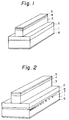
- Fig. 1 is a perspective view of a conventional electroabsorption type optical modulation element as shown in GB-A-2 187 300.
- an n-type InP substrate 1 there are laminated an n-InGaAsP modulating waveguide layer 2, a mesa-shaped p-type InP clad layer 3, and a p-type InGaAsP contact layer 4, and a p-side electrode 5 and an n-side electrode 6 are deposited over the p-type InGaAsP contact layer 4 and the n-type InP substrate 1, respectively.
- this optical modulation element With this optical modulation element, a minus voltage applied to the p-side electrode 5 and a plus voltage applied to the n-side electrode 6, respectively, are varied by applying light to the InGaAsP modulating waveguide layer 2 so that its absorption coefficient is varied, thereby making it possible to modulate the intensity of the emitted light. It is essential to the electroabsorption type optical modulation element that it is capable of low-voltage modulation, high-speed modulation and suppression of an increase in the spectral width during the high-speed modulation.
- the optical modulation element of this type permits the high-speed modulation and the suppression of an increase in the spectral width because the closer to the photon energy h ⁇ of incident light the forbidden band energy Eg of the InGaAsP modulating waveguide layer 2 is, the more greatly its absorption coefficient can be varied by the lower voltage and the more the device length L (i.e., the length of the InGaAsP modulating waveguide layer 2 from the light receiving end face to the light emitting end face thereof) can be reduced.
- the intensity of light incident on an optical modulator and the absorption coefficient and the optical confinement coefficient of the optical waveguide layer be represented by I (0) , ⁇ and ⁇ , respectively
- the number of carriers absorbed per unit length is substantially in proportion to I (x) , and the number of carriers absorbed in the vicinity of the light receiving end is abnormally larger than the number of carriers absorbed in the vicinity of the light emitting end.
- the absorbed carrier distribution even if nonuniform, have no influence on the band structure, and hence does not pose any problem, but when the intensity of incident light increases excess carriers absorbed near the light receiving end cancels the applied electric field, affecting the modulating voltage and the modulation speed.
- the present inventors considered that if ⁇ I (x) in Eq. (2) would be held almost constant so that carriers of substantially the same number are absorbed over the entire length of the optical waveguide layer from the light incident end to the light emitting end thereof, effective optical modulation could be achieved without generating excess carriers which would be nonuniformly distributed locally. That is to say, by making the absorption coefficient ⁇ to be small at a place where the amount of light is large and to be large at a place where the amount of light is small, a high performance optical modulation element can be implemented which is free from a decrease in the modulation bandwidth and an increase in the modulating voltage when high intensity light is incident on the element.
- Fig. 2 illustrates schematically an embodiment of an optical modulation element of the present invention.
- Irregularities are formed in the surface of an n+-InP substrate 1 which has an impurity concentration of 5 x 1018 cm ⁇ 3 or so and on which are laminated an n ⁇ InP layer (a lower clad layer) 8 having an impurity concentration of approximately 1 x 1015 cm ⁇ 3 an n ⁇ -InGaAsP (emitted light wavelength: about 1.45 ⁇ m) optical waveguide layer 2 about 0.25 ⁇ m, a p+-InP clad layer (an upper clad layer) 3, and a p+-InGaAsP contact layer 4.
- a p-side electrode 5 and an n-side electrode 6 are deposited over the p-type InGaAsP contact layer 4 and the n-type InP substrate 1, respectively.
- the thicknesses of those portions of the n ⁇ -InP layer 8 overlying the convexities of the irregularities 7 are around 0.08 ⁇ m and the element length is of 360 ⁇ m.
- the concavities in the surface of the n-type InP substrate 1 have length of about 3 ⁇ m (in width in the direction of travel of light) and depths of 0.3 ⁇ m.
- the lengths of the convexities are 2.35 ⁇ m (four times), 3 ⁇ m (three times), 4.5 ⁇ m (three times), 6.1 ⁇ m (twice), 7.7 ⁇ m (twice), 9 ⁇ m (twice), and 20 ⁇ m (once) at intervals of approximately 20 ⁇ m, and the subsequent convexities have lengths of 220 ⁇ m.
- the irregularities 7 need only to be formed so that their invervals become longer stepwise toward the light emitting end face from the light incident end face.
- the effective width of a depletion layer decreases in the direction of travel of light, and consequently, the electric field increases accordingly.
- the mean electric field intensity in the optical waveguide layer 2 under application of a voltage of two volts changes from 40 KV to 60 KV toward the light emitting end from the light incident end, and the absorption coefficient ⁇ for incident light of a 1.55 ⁇ m increases from 50 cm ⁇ 1 to 160 cm ⁇ 1 in the direction of travel of light.
- the light intensity decreases by 10% each at 20 ⁇ m intervals and the absorption coefficient increases by 10% each, the number of carriers absorbed per unit length remains unchanged over a region from the position of 100% light intensity to the position of 30% light intensity. After dropping to 30% the light intensity is reduced down in 1/100 by the 220 ⁇ m length convexity.
- a 3 dB bandwidth is 10 GHz or more.
- the numbers of carriers absorbed are equal at almost all points from the light incident end to the point where the light intensity is reduced to 30%; namely, the number of carriers absorbed at every point is made equal. Accordingly, there is no possibility that carriers are excessively absorbed locally near the light incident end where the light intensity is high as in the prior art example, and hence no space charge effect will be produced. This permits the implementation of a high performance optical modulation element which is free from deterioration of its characteristics even when high intensity light is applied.
- the lengths of the n+-InP convexities different in impurity concentration from the n ⁇ -InP concavities are changed at intervals of 20 ⁇ m, they may also be varied continuously. Further, in Embodiment 1 the numbers of carriers absorbed at all points from the light incident end to the position where the light intensity decreases to 30% are made equal to one another, but it is also possible to adopt a structure in which the same number of carriers are absorbed in all regions.
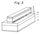
- Fig. 3 schematically illustrates another embodiment of the optical modulation element of the present invention.
- This embodiment differs from the prior art example in that n ⁇ -InGaAsP (emitted light wavelength: 1.2 ⁇ m) layers 9, which has a thickness of 0.3 ⁇ m and a length of 3 ⁇ m, and p+-InGaAsP layers 10, which has a thickness of 0.3 ⁇ m but different in length, are alternately disposed between the p+-InP upper clad layer 3 and the optical waveguide layer 2 in the direction of travel of light so as to vary the absorption coefficient in that direction.
- n ⁇ -InGaAsP emit light wavelength: 1.2 ⁇ m
- p+-InGaAsP layers 10 which has a thickness of 0.3 ⁇ m but different in length
- the p+-InGaAsP layers 10 are formed longer toward the light emitting end as is the case with the n+-InP covexities in the embodiment shown in Fig. 2.
- the lengths (the widths in the direction of travel of light) of the n ⁇ -InGaAsP layers 9 are made constant and the lengths of the p+-InGaAsP layers 10 are changed, but it is also possible to employ a structure in which the lengths of the n ⁇ -InGaAsP layers 9 decrease toward the light emitting end from the light incident end.
- the number of carriers absorbed is constant at all places of light intensity lowering from 100% to 30% as in the embodiment of Fig. 2 and it is likely that the space charge effect is produced by locally excessive absorption of carriers at the light incident end as in the prior art example. Accordingly, it is possible to implement a high performance optical modulation element which is free from deterioration of its characteristics even when the intensity of light incident thereon is high.
- the conductivity type of the optical waveguide layer may also be the p ⁇ -type.
- the present invention has been described in connection with the case of employing materials of the InGaAsP/InP series, the invention is applicable as well to materials of the AlGaAs/GaAs, AlGaAs/InP series, etc. Furthermore, it is also possible to use multiple quantum well layers of such materials, in which case the energy gap mentioned in the above is an effective energy gap dependent on the quantum level. While in the above the stripe structure for transverse mode stabilization has been described to be the stripe loaded type, prior art structures such as a buried stripe structure, a ridge waveguide stripe structure, etc. can all be employed.
- the optical modulation element is constructed so that the absorption coefficient is small near the light incident end where the light intensity is high but large near the light emitting end so as to make constant the number of carriers absorbed per unit length. Accordingly, even if the light intensity is increased, there is no possibility of local generation of excess carriers which leads to an increase in the modulating voltage and a decrease in the modulation bandwidth by the space charge effect.
- the present invention offers a high performance optical modulation element which permits low-voltage, high-speed optical modulation.
- the method of forming the irregularities in the surface of the n+-InP substrate and depositing thereon the n ⁇ -InP layer, the n ⁇ -InGaAsP layer, etc. is advantageous in that these layers can be grown by one step. This allows ease in the manufacture of the optical modulation element which retains high-performance characteristics when high intensity light is incident thereon.
- the structure in which InGaAsP layers of different conductivity types are formed unevenly on the n ⁇ -InGaAsP waveguide layer 2, also provides a high performance optical modulation element, because the irregularities can be formed by thermal diffusion and is excellent in crystallinity.
- the optical modulation element of the present invention uses the same optical waveguide mechanism as that of the prior art example but controls only the electrical property (conductivity) of the waveguide mechanism to gradually increase the absorption coefficient in the direction of travel of light, so that no optical loss such as mode transformation will be incurred and no characteristics will be degraded even when the intensity of incident light is high.
- the optical modulation element of the present invention is applicable to ultra-high-speed, long-distance fiber optic communication in the Giga-bit band, and hence is of great utility.
Landscapes
- Physics & Mathematics (AREA)
- Nonlinear Science (AREA)
- General Physics & Mathematics (AREA)
- Optics & Photonics (AREA)
- Optical Integrated Circuits (AREA)
- Optical Modulation, Optical Deflection, Nonlinear Optics, Optical Demodulation, Optical Logic Elements (AREA)
- Photo Coupler, Interrupter, Optical-To-Optical Conversion Devices (AREA)
- Amplitude Modulation (AREA)
Description
- The present invention relates to an optical modulation element which modulates light incident thereon from outside.
- Fiber optic communication technology has developed through utilization of the ultra-low loss property of optical fibers and the ultra-wide band property intrinsic to light, and fiber optic communication is now under study for longer-distance, large-capacity transmission in many countries. Now that the transmission loss of the optical fiber has reached a theoretical limit, studies for higher-speed, larger-capacity transmission are particularly important.
- At present, high-speed ON-OFF control of an optical signal is generally effected by a method of directly modulating a semiconductor laser. With the direct modulation system, however, since a current of the semiconductor laser serving as an oscillation element is caused to vary at high speed, its oscillation wavelength changes significantly with time, resulting in the spectral width of oscillation becoming abnormally wider than the spectral width of the modulation band. In consequence, in a long-distance or high-speed transmission optical pulses to be received are distorted largely through the influence of wavelength dispersion by the optical fiber, and hence no excellent transmission characteristic can be obtained. To avoid this, a method of modulating the semiconductor laser at high speed by an external optical modulation element while holding the laser output constant has recently been studied.
- As the optical modulation element, an optical modulation element using a ferrodielectric substance such as LiNbO₃ and an optical modulation element which can be integrated monolithically with a DFB laser or similar single-wavelength semiconductor laser have been proposed. Among these optical modulation elements, the latter electro-absorption type optical modulation element in which an electric field is applied to a modulating waveguide layer to perform an intensity modulation of the output light by an electro-absorption effect is regarded as the most promising element.
- However, the conventional electro-absorption type optical modulation element is capable of low-voltage modulation, high-speed operation and narrow-band oscillation when the intensity of incident light is low, but it is defective in that these characteristics significantly deteriorate when the light intensity is raised to a practical value of several mW.
- It is an object of the present invention, in order to solve the above-mentioned defect of prior art, to provide an optical modulation element which is capable of low-voltage, high-speed modulation in case of increasing the intensity of incident light.
- According to the present invention there is provided an optical modulation element which has, between a pair of electrodes and on a substrate with or without an intermediate lower clad layer, an optical waveguide layer of a low impurity concentration, and an upper clad layer of a refractive index smaller than that of the optical waveguide layer, and in which light of a constant intensity incident on a light incident end face of the optical waveguide layer is intensity-modulated by changing the absorption coefficient of the optical waveguide layer by means of an electric field applied thereto across the electrodes so that the thus modulated light is emitted from a light emitting end face of the optical waveguide layer,
characterised by a layer which is in contact with at least one of the lower and upper clad layers and consists of a plurality of low impurity concentration regions and a plurality of high impurity concentration regions disposed alternately with each other in the direction of travel of light in such a manner that the high impurity concentration regions are progressively longer in the direction of travel of light. - A feature of embodiments of the optical modulation element of the present invention is that a clad layer overlaying or underlying an optical waveguide layer is formed by a plurality of low impurity concentration regions and a plurality of high impurity concentration regions in such a manner that the high impurity concentration regions are progressively longer in the direction of travel of light to increase the electric field intensity in the waveguide accordingly, thereby limiting variations in the number of carriers to be absorbed per unit length.
- Embodiments of the present invention will now be described, by way of example, in comparison with prior art and with reference to the accompanying drawings, in which:
- Fig. 1 is a schematic diagram of a conventional electroabsorption type optical modulation element; and
- Figs. 2 and 3 are schematic diagrams illustrating optical modulation element structures of embodiments of the present invention.
- To make differences between prior art and the present invention clear, an example of prior art will first be described.
- Fig. 1 is a perspective view of a conventional electroabsorption type optical modulation element as shown in GB-A-2 187 300. On an n-type InP substrate 1 there are laminated an n-InGaAsP modulating
waveguide layer 2, a mesa-shaped p-typeInP clad layer 3, and a p-typeInGaAsP contact layer 4, and a p-side electrode 5 and an n-side electrode 6 are deposited over the p-typeInGaAsP contact layer 4 and the n-type InP substrate 1, respectively. - With this optical modulation element, a minus voltage applied to the p-
side electrode 5 and a plus voltage applied to the n-side electrode 6, respectively, are varied by applying light to the InGaAsP modulatingwaveguide layer 2 so that its absorption coefficient is varied, thereby making it possible to modulate the intensity of the emitted light. It is essential to the electroabsorption type optical modulation element that it is capable of low-voltage modulation, high-speed modulation and suppression of an increase in the spectral width during the high-speed modulation. It has been considered, up to now, that the optical modulation element of this type permits the high-speed modulation and the suppression of an increase in the spectral width because the closer to the photon energy hν of incident light the forbidden band energy Eg of the InGaAsP modulatingwaveguide layer 2 is, the more greatly its absorption coefficient can be varied by the lower voltage and the more the device length L (i.e., the length of the InGaAsP modulatingwaveguide layer 2 from the light receiving end face to the light emitting end face thereof) can be reduced. Accordingly, attention has been paid only to a difference between the both energies, ΔEg(Eg - hν), in the past, and it has been considered that an optical modulation element of high performance could be implemented by setting the energy difference ΔEg to 30 to 40 meV. It has been found, however, that although the conventional optical modulation element exhibits excellent characteristics in the modulating voltage, the modulation bandwidth and the spectral width of oscillation when the intensity of incident light is about 100 µW or lower, the modulating voltage markedly increases and the modulation bandwidth also decreases as the intensity of incident light exceeds 0.1 mW. - Close studies of phenomena such as an increase in the modulating voltage and a decrease in the modulation bandwidth caused by an increase in the intensity of incident light have revealed that these characteristic deteriorations largely depend on the energy difference, (

- The above experimental results indicate that when the intensity of incident light is high, a space charge effect by excess carriers, which occurs only in a very small region near the light receiving end where the light intensity is very high, lowers the field intensity and decreases the modulation speed.
- The principle of the present invention will hereinafter be described.
- Letting the intensity of light incident on an optical modulator and the absorption coefficient and the optical confinement coefficient of the optical waveguide layer be represented by I(0), α and Γ, respectively, the light intensity I(x) at a distance x from the light receiving end face can be expressed as follows:

and the amount of light absorbed per unit length is as follows:
Eq. (2) is proportional to the number of carriers absorbed per unit length. In the conventional modulation element, since α and Γ are constant, the number of carriers absorbed per unit length is substantially in proportion to I(x), and the number of carriers absorbed in the vicinity of the light receiving end is abnormally larger than the number of carriers absorbed in the vicinity of the light emitting end. In a case where the intensity of incident light is low, the absorbed carrier distribution, even if nonuniform, have no influence on the band structure, and hence does not pose any problem, but when the intensity of incident light increases excess carriers absorbed near the light receiving end cancels the applied electric field, affecting the modulating voltage and the modulation speed. - In view of the above, the present inventors considered that if αΓI(x) in Eq. (2) would be held almost constant so that carriers of substantially the same number are absorbed over the entire length of the optical waveguide layer from the light incident end to the light emitting end thereof, effective optical modulation could be achieved without generating excess carriers which would be nonuniformly distributed locally. That is to say, by making the absorption coefficient α to be small at a place where the amount of light is large and to be large at a place where the amount of light is small, a high performance optical modulation element can be implemented which is free from a decrease in the modulation bandwidth and an increase in the modulating voltage when high intensity light is incident on the element.
- With reference to the accompanying drawings, embodiments of the present invention will hereinafter be described in detail.
- Fig. 2 illustrates schematically an embodiment of an optical modulation element of the present invention. Irregularities are formed in the surface of an n⁺-InP substrate 1 which has an impurity concentration of 5 x 10¹⁸ cm⁻³ or so and on which are laminated an n⁻InP layer (a lower clad layer) 8 having an impurity concentration of approximately 1 x 10¹⁵ cm⁻³ an n⁻-InGaAsP (emitted light wavelength: about 1.45 µm)
optical waveguide layer 2 about 0.25 µm, a p⁺-InP clad layer (an upper clad layer) 3, and a p⁺-InGaAsP contact layer 4. Further, a p-side electrode 5 and an n-side electrode 6 are deposited over the p-typeInGaAsP contact layer 4 and the n-type InP substrate 1, respectively. Incidentally, the thicknesses of those portions of the n⁻-InP layer 8 overlying the convexities of the irregularities 7 are around 0.08 µm and the element length is of 360 µm. - The concavities in the surface of the n-type InP substrate 1 have length of about 3 µm (in width in the direction of travel of light) and depths of 0.3 µm. The lengths of the convexities are 2.35 µm (four times), 3 µm (three times), 4.5 µm (three times), 6.1 µm (twice), 7.7 µm (twice), 9 µm (twice), and 20 µm (once) at intervals of approximately 20 µm, and the subsequent convexities have lengths of 220 µm.
- In other words, the irregularities 7 need only to be formed so that their invervals become longer stepwise toward the light emitting end face from the light incident end face.
- With this structure, the effective width of a depletion layer decreases in the direction of travel of light, and consequently, the electric field increases accordingly. The mean electric field intensity in the
optical waveguide layer 2 under application of a voltage of two volts changes from 40 KV to 60 KV toward the light emitting end from the light incident end, and the absorption coefficient α for incident light of a 1.55 µm increases from 50 cm⁻¹ to 160 cm⁻¹ in the direction of travel of light. Moreover, since the light intensity decreases by 10% each at 20 µm intervals and the absorption coefficient increases by 10% each, the number of carriers absorbed per unit length remains unchanged over a region from the position of 100% light intensity to the position of 30% light intensity. After dropping to 30% the light intensity is reduced down in 1/100 by the 220 µm length convexity. A 3 dB bandwidth is 10 GHz or more. - According to this embodiment, the numbers of carriers absorbed are equal at almost all points from the light incident end to the point where the light intensity is reduced to 30%; namely, the number of carriers absorbed at every point is made equal. Accordingly, there is no possibility that carriers are excessively absorbed locally near the light incident end where the light intensity is high as in the prior art example, and hence no space charge effect will be produced. This permits the implementation of a high performance optical modulation element which is free from deterioration of its characteristics even when high intensity light is applied.
- While in the above the lengths of the n⁺-InP convexities different in impurity concentration from the n⁻-InP concavities are changed at intervals of 20 µm, they may also be varied continuously. Further, in Embodiment 1 the numbers of carriers absorbed at all points from the light incident end to the position where the light intensity decreases to 30% are made equal to one another, but it is also possible to adopt a structure in which the same number of carriers are absorbed in all regions.
- Fig. 3 schematically illustrates another embodiment of the optical modulation element of the present invention.
- This embodiment differs from the prior art example in that n⁻-InGaAsP (emitted light wavelength: 1.2 µm)
layers 9, which has a thickness of 0.3 µm and a length of 3 µm, and p⁺-InGaAsP layers 10, which has a thickness of 0.3 µm but different in length, are alternately disposed between the p⁺-InPupper clad layer 3 and theoptical waveguide layer 2 in the direction of travel of light so as to vary the absorption coefficient in that direction. - The p⁺-
InGaAsP layers 10 are formed longer toward the light emitting end as is the case with the n⁺-InP covexities in the embodiment shown in Fig. 2. - In the above the lengths (the widths in the direction of travel of light) of the n⁻-
InGaAsP layers 9 are made constant and the lengths of the p⁺-InGaAsP layers 10 are changed, but it is also possible to employ a structure in which the lengths of the n⁻-InGaAsP layers 9 decrease toward the light emitting end from the light incident end. - Also in this embodiment, the number of carriers absorbed is constant at all places of light intensity lowering from 100% to 30% as in the embodiment of Fig. 2 and it is likely that the space charge effect is produced by locally excessive absorption of carriers at the light incident end as in the prior art example. Accordingly, it is possible to implement a high performance optical modulation element which is free from deterioration of its characteristics even when the intensity of light incident thereon is high.
- The conductivity type of the optical waveguide layer may also be the p⁻-type. Although the present invention has been described in connection with the case of employing materials of the InGaAsP/InP series, the invention is applicable as well to materials of the AlGaAs/GaAs, AlGaAs/InP series, etc. Furthermore, it is also possible to use multiple quantum well layers of such materials, in which case the energy gap mentioned in the above is an effective energy gap dependent on the quantum level. While in the above the stripe structure for transverse mode stabilization has been described to be the stripe loaded type, prior art structures such as a buried stripe structure, a ridge waveguide stripe structure, etc. can all be employed.
- As described above, in accordance with the present invention, the optical modulation element is constructed so that the absorption coefficient is small near the light incident end where the light intensity is high but large near the light emitting end so as to make constant the number of carriers absorbed per unit length. Accordingly, even if the light intensity is increased, there is no possibility of local generation of excess carriers which leads to an increase in the modulating voltage and a decrease in the modulation bandwidth by the space charge effect. Thus, the present invention offers a high performance optical modulation element which permits low-voltage, high-speed optical modulation.
- The method of forming the irregularities in the surface of the n⁺-InP substrate and depositing thereon the n⁻-InP layer, the n⁻-InGaAsP layer, etc. is advantageous in that these layers can be grown by one step. This allows ease in the manufacture of the optical modulation element which retains high-performance characteristics when high intensity light is incident thereon.
- The structure, in which InGaAsP layers of different conductivity types are formed unevenly on the n⁻-
InGaAsP waveguide layer 2, also provides a high performance optical modulation element, because the irregularities can be formed by thermal diffusion and is excellent in crystallinity. - The optical modulation element of the present invention uses the same optical waveguide mechanism as that of the prior art example but controls only the electrical property (conductivity) of the waveguide mechanism to gradually increase the absorption coefficient in the direction of travel of light, so that no optical loss such as mode transformation will be incurred and no characteristics will be degraded even when the intensity of incident light is high.
- The optical modulation element of the present invention is applicable to ultra-high-speed, long-distance fiber optic communication in the Giga-bit band, and hence is of great utility.
Claims (5)
- An optical modulation element which has, between a pair of electrodes (5,6) and on a substrate (1) with or without an intermediate lower clad layer (8), an optical waveguide layer (2) of a low impurity concentration, and an upper clad layer (3) of a refractive index smaller than that of the optical waveguide layer, and in which light of a constant intensity incident on a light incident end face of the optical waveguide layer is intensity-modulated by changing the absorption coefficient of the optical waveguide layer by means of an electric field applied thereto across the electrodes so that the thus modulated light is emitted from a light emitting end face of the optical waveguide layer,
characterised by a layer which is in contact with at least one of the lower and upper clad layers (8,3) and consists of a plurality of low impurity concentration regions (8;9) and a plurality of high impurity concentration regions (1;10) disposed alternately with each other in the direction of travel of light in such a manner that the high impurity concentration regions (1;10) are progressively longer in the direction of travel of light. - An optical modulation element according to claim 1, characterised in that said layer is composed of high impurity concentration regions formed by irregularities (7) comprising convexities and concavities in the surface of said substrate (1) and low impurity concentration regions buried in said concavities.
- An optical modulation element according to claim 2 characterised in that the lengths of said convexities increase continuously or discontinuously toward the light emitting end face from the light incident end face of the optical waveguide layer.
- An optical modulation element according to claim 1, characterised in that said layer is provided as an intermediate layer between the optical waveguide layer (2) and the upper clad layer (3) and is composed of a plurality of low impurity concentration clad layer regions (9) of a first conductivity type and a plurality of high impurity concentration clad layer regions (10) of a second conductivity type which are disposed alternately with each other.
- An optical modulation element according to claim 4, characterised in that the lengths of the high impurity concentration clad layer regions (10) increase continuously or discontinuously toward the light emitting end face from the light incident end face of the optical waveguide layer.
Applications Claiming Priority (2)
| Application Number | Priority Date | Filing Date | Title |
|---|---|---|---|
| JP195840/88 | 1988-08-05 | ||
| JP19584088A JPH0816743B2 (en) | 1988-08-05 | 1988-08-05 | Light modulation element |
Publications (3)
| Publication Number | Publication Date |
|---|---|
| EP0354058A2 EP0354058A2 (en) | 1990-02-07 |
| EP0354058A3 EP0354058A3 (en) | 1990-08-01 |
| EP0354058B1 true EP0354058B1 (en) | 1994-01-26 |
Family
ID=16347881
Family Applications (1)
| Application Number | Title | Priority Date | Filing Date |
|---|---|---|---|
| EP89307959A Expired - Lifetime EP0354058B1 (en) | 1988-08-05 | 1989-08-04 | Optical modulation element |
Country Status (3)
| Country | Link |
|---|---|
| US (1) | US4946243A (en) |
| EP (1) | EP0354058B1 (en) |
| JP (1) | JPH0816743B2 (en) |
Families Citing this family (6)
| Publication number | Priority date | Publication date | Assignee | Title |
|---|---|---|---|---|
| US4913506A (en) * | 1988-02-26 | 1990-04-03 | Kokusai Denshin Denwa Kabushiki Kaisha | Optical modulation device |
| JPH0816744B2 (en) * | 1988-12-01 | 1996-02-21 | 国際電信電話株式会社 | Light modulation element |
| FI84869C (en) * | 1990-06-11 | 1992-01-27 | Planar Int Oy | Matrix film structure in particular for the electroluminescence display unit |
| US5054871A (en) * | 1990-07-02 | 1991-10-08 | Bell Communications Research, Inc. | Semiconductor waveguide and impedance-matched detector |
| JP2820138B2 (en) * | 1996-11-26 | 1998-11-05 | 日本電気株式会社 | Light modulator |
| JP5906210B2 (en) * | 2013-03-26 | 2016-04-20 | 日本電信電話株式会社 | Light modulator |
Family Cites Families (3)
| Publication number | Priority date | Publication date | Assignee | Title |
|---|---|---|---|---|
| JPS60107019A (en) * | 1983-11-16 | 1985-06-12 | Hitachi Ltd | Waveguide type optical modulator |
| JPH0690369B2 (en) * | 1986-02-21 | 1994-11-14 | 国際電信電話株式会社 | Semiconductor optical modulator |
| US4772854A (en) * | 1986-12-24 | 1988-09-20 | Bell Communications Research, Inc. | All optical repeater |
-
1988
- 1988-08-05 JP JP19584088A patent/JPH0816743B2/en not_active Expired - Fee Related
-
1989
- 1989-07-28 US US07/387,511 patent/US4946243A/en not_active Expired - Lifetime
- 1989-08-04 EP EP89307959A patent/EP0354058B1/en not_active Expired - Lifetime
Also Published As
| Publication number | Publication date |
|---|---|
| JPH0816743B2 (en) | 1996-02-21 |
| EP0354058A3 (en) | 1990-08-01 |
| JPH0244311A (en) | 1990-02-14 |
| US4946243A (en) | 1990-08-07 |
| EP0354058A2 (en) | 1990-02-07 |
Similar Documents
| Publication | Publication Date | Title |
|---|---|---|
| US5801872A (en) | Semiconductor optical modulation device | |
| US5339370A (en) | Optical modulator and optical communication system utilizing the same | |
| WO1993003411A1 (en) | Separate confinement electroabsorption modulator | |
| US6100543A (en) | Electro-absorption type semiconductor optical modulator having a quantum well structure | |
| US5703974A (en) | Semiconductor photonic integrated circuit and fabrication process therefor | |
| US4913506A (en) | Optical modulation device | |
| CA2398287A1 (en) | Improved optoelectronic device | |
| US7142342B2 (en) | Electroabsorption modulator | |
| US4946243A (en) | Optical modulation element | |
| US4991921A (en) | Pn junction optical modulating device having a buffer layer with small energy gap | |
| US20040052282A1 (en) | Semiconductor laser device | |
| US4811353A (en) | Semiconductor optical modulator | |
| JPH08248364A (en) | Light intensity modulation element and semiconductor laser with light intensity modulation element | |
| JP7402014B2 (en) | Optical semiconductor elements, optical semiconductor devices | |
| JPH06100737B2 (en) | Light modulator | |
| JPH07176822A (en) | Semiconductor light source and its manufacture | |
| JPH058878B2 (en) | ||
| JPH10144950A (en) | Semiconductor light receiving device | |
| US6661557B2 (en) | Optical modulator | |
| JPH02212804A (en) | Optical semiconductor element and production thereof | |
| KR100294626B1 (en) | Field Absorption Optical Modulator with N (-)-I-N (+) Structure | |
| JP2890644B2 (en) | Manufacturing method of integrated optical modulator | |
| EP1849037B1 (en) | Optical modulator | |
| JPH03192788A (en) | Integrated optical modulator | |
| JPH01217417A (en) | Optical modulation element |
Legal Events
| Date | Code | Title | Description |
|---|---|---|---|
| PUAI | Public reference made under article 153(3) epc to a published international application that has entered the european phase |
Free format text: ORIGINAL CODE: 0009012 |
|
| AK | Designated contracting states |
Kind code of ref document: A2 Designated state(s): FR GB |
|
| PUAL | Search report despatched |
Free format text: ORIGINAL CODE: 0009013 |
|
| AK | Designated contracting states |
Kind code of ref document: A3 Designated state(s): FR GB |
|
| 17P | Request for examination filed |
Effective date: 19900731 |
|
| 17Q | First examination report despatched |
Effective date: 19920415 |
|
| GRAA | (expected) grant |
Free format text: ORIGINAL CODE: 0009210 |
|
| AK | Designated contracting states |
Kind code of ref document: B1 Designated state(s): FR GB |
|
| ET | Fr: translation filed | ||
| PLBE | No opposition filed within time limit |
Free format text: ORIGINAL CODE: 0009261 |
|
| STAA | Information on the status of an ep patent application or granted ep patent |
Free format text: STATUS: NO OPPOSITION FILED WITHIN TIME LIMIT |
|
| 26N | No opposition filed | ||
| REG | Reference to a national code |
Ref country code: GB Ref legal event code: IF02 |
|
| PGFP | Annual fee paid to national office [announced via postgrant information from national office to epo] |
Ref country code: GB Payment date: 20040730 Year of fee payment: 16 |
|
| PGFP | Annual fee paid to national office [announced via postgrant information from national office to epo] |
Ref country code: FR Payment date: 20040809 Year of fee payment: 16 |
|
| PG25 | Lapsed in a contracting state [announced via postgrant information from national office to epo] |
Ref country code: GB Free format text: LAPSE BECAUSE OF NON-PAYMENT OF DUE FEES Effective date: 20050804 |
|
| GBPC | Gb: european patent ceased through non-payment of renewal fee |
Effective date: 20050804 |
|
| PG25 | Lapsed in a contracting state [announced via postgrant information from national office to epo] |
Ref country code: FR Free format text: LAPSE BECAUSE OF NON-PAYMENT OF DUE FEES Effective date: 20060428 |
|
| REG | Reference to a national code |
Ref country code: FR Ref legal event code: ST Effective date: 20060428 |