EP0353530B1 - Method for differentiating between electronic circuits with non-volatile memories - Google Patents
Method for differentiating between electronic circuits with non-volatile memories Download PDFInfo
- Publication number
- EP0353530B1 EP0353530B1 EP89113081A EP89113081A EP0353530B1 EP 0353530 B1 EP0353530 B1 EP 0353530B1 EP 89113081 A EP89113081 A EP 89113081A EP 89113081 A EP89113081 A EP 89113081A EP 0353530 B1 EP0353530 B1 EP 0353530B1
- Authority
- EP
- European Patent Office
- Prior art keywords
- specific identifier
- volatile memory
- specific
- test
- electronic circuits
- Prior art date
- Legal status (The legal status is an assumption and is not a legal conclusion. Google has not performed a legal analysis and makes no representation as to the accuracy of the status listed.)
- Expired - Lifetime
Links
Images
Classifications
-
- G—PHYSICS
- G07—CHECKING-DEVICES
- G07F—COIN-FREED OR LIKE APPARATUS
- G07F7/00—Mechanisms actuated by objects other than coins to free or to actuate vending, hiring, coin or paper currency dispensing or refunding apparatus
- G07F7/08—Mechanisms actuated by objects other than coins to free or to actuate vending, hiring, coin or paper currency dispensing or refunding apparatus by coded identity card or credit card or other personal identification means
- G07F7/10—Mechanisms actuated by objects other than coins to free or to actuate vending, hiring, coin or paper currency dispensing or refunding apparatus by coded identity card or credit card or other personal identification means together with a coded signal, e.g. in the form of personal identification information, like personal identification number [PIN] or biometric data
- G07F7/1008—Active credit-cards provided with means to personalise their use, e.g. with PIN-introduction/comparison system
-
- G—PHYSICS
- G06—COMPUTING OR CALCULATING; COUNTING
- G06Q—INFORMATION AND COMMUNICATION TECHNOLOGY [ICT] SPECIALLY ADAPTED FOR ADMINISTRATIVE, COMMERCIAL, FINANCIAL, MANAGERIAL OR SUPERVISORY PURPOSES; SYSTEMS OR METHODS SPECIALLY ADAPTED FOR ADMINISTRATIVE, COMMERCIAL, FINANCIAL, MANAGERIAL OR SUPERVISORY PURPOSES, NOT OTHERWISE PROVIDED FOR
- G06Q20/00—Payment architectures, schemes or protocols
- G06Q20/30—Payment architectures, schemes or protocols characterised by the use of specific devices or networks
- G06Q20/34—Payment architectures, schemes or protocols characterised by the use of specific devices or networks using cards, e.g. integrated circuit [IC] cards or magnetic cards
- G06Q20/341—Active cards, i.e. cards including their own processing means, e.g. including an IC or chip
-
- G—PHYSICS
- G06—COMPUTING OR CALCULATING; COUNTING
- G06Q—INFORMATION AND COMMUNICATION TECHNOLOGY [ICT] SPECIALLY ADAPTED FOR ADMINISTRATIVE, COMMERCIAL, FINANCIAL, MANAGERIAL OR SUPERVISORY PURPOSES; SYSTEMS OR METHODS SPECIALLY ADAPTED FOR ADMINISTRATIVE, COMMERCIAL, FINANCIAL, MANAGERIAL OR SUPERVISORY PURPOSES, NOT OTHERWISE PROVIDED FOR
- G06Q20/00—Payment architectures, schemes or protocols
- G06Q20/30—Payment architectures, schemes or protocols characterised by the use of specific devices or networks
- G06Q20/34—Payment architectures, schemes or protocols characterised by the use of specific devices or networks using cards, e.g. integrated circuit [IC] cards or magnetic cards
- G06Q20/355—Personalisation of cards for use
-
- G—PHYSICS
- G07—CHECKING-DEVICES
- G07F—COIN-FREED OR LIKE APPARATUS
- G07F7/00—Mechanisms actuated by objects other than coins to free or to actuate vending, hiring, coin or paper currency dispensing or refunding apparatus
- G07F7/08—Mechanisms actuated by objects other than coins to free or to actuate vending, hiring, coin or paper currency dispensing or refunding apparatus by coded identity card or credit card or other personal identification means
- G07F7/0806—Details of the card
- G07F7/0813—Specific details related to card security
- G07F7/082—Features insuring the integrity of the data on or in the card
-
- G—PHYSICS
- G07—CHECKING-DEVICES
- G07F—COIN-FREED OR LIKE APPARATUS
- G07F7/00—Mechanisms actuated by objects other than coins to free or to actuate vending, hiring, coin or paper currency dispensing or refunding apparatus
- G07F7/08—Mechanisms actuated by objects other than coins to free or to actuate vending, hiring, coin or paper currency dispensing or refunding apparatus by coded identity card or credit card or other personal identification means
- G07F7/0806—Details of the card
- G07F7/0833—Card having specific functional components
- G07F7/084—Additional components relating to data transfer and storing, e.g. error detection, self-diagnosis
-
- G—PHYSICS
- G01—MEASURING; TESTING
- G01R—MEASURING ELECTRIC VARIABLES; MEASURING MAGNETIC VARIABLES
- G01R31/00—Arrangements for testing electric properties; Arrangements for locating electric faults; Arrangements for electrical testing characterised by what is being tested not provided for elsewhere
- G01R31/28—Testing of electronic circuits, e.g. by signal tracer
- G01R31/317—Testing of digital circuits
- G01R31/3181—Functional testing
- G01R31/319—Tester hardware, i.e. output processing circuits
-
- G—PHYSICS
- G06—COMPUTING OR CALCULATING; COUNTING
- G06F—ELECTRIC DIGITAL DATA PROCESSING
- G06F11/00—Error detection; Error correction; Monitoring
- G06F11/006—Identification
Definitions
- the invention relates to a method for differentiating monolithically integrated circuits with at least one non-volatile memory according to the preamble of claim 1.
- Monolithically integrated circuits which contain a non-volatile memory and in which it is necessary to differentiate the individual chips are known from EP-OS 0 207 320, EP-OS 0127 809, FR-PS 23 11 360, EP-OS 0 128 362 and DE-PS 26 21 271 known. These are the integrated electronic circuits of so-called chip cards, or chip charrying cards, as described in the article "Intelligence on plastic, security systems with chip carrying cards" by H. Lambert and M. Schmötzer in the electronics magazine February 3, 1986. It is also known, inter alia, from EP-OS 0 123 177 to block the write and erasability of certain memory areas by reducing the maximum permissible voltage level of the corresponding programming lines.
- circuits have in common that they contain a secret code in a non-volatile, more or less inaccessible memory area, which serves either as a basis for encryption or decryption or directly as a basis for comparison for another comparison code, in particular to be entered by the user.
- Card-specific electrical features can also be used in conjunction with a secret algorithm for generating card-specific secret keys.
- the correct secret key that matches the card feature also allows such cards to be authenticated. However, if someone had researched a valid secret code, he would in principle be able to recreate them as real recognizable chip cards with the same characteristic or the same secret code.
- the object of the invention is to provide a method for the practical differentiation of at least one non-volatile memory-containing monolithic integrated circuits during the manufacturing process of these integrated circuits.
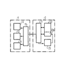
- the figure shows a standard tester 1, which among other things consists of a tester logic circuit 11, a license plate input unit 12, a test program input unit 13 and a blocking program input unit 14, and an electronic circuit 2, in particular a control logic circuit 21, a blocking device 23 and a license plate memory 22a, which in particular is part of a non-volatile memory 22 which is intended to hold the specific identifier.
- a standard tester which among other things consists of a tester logic circuit 11, a license plate input unit 12, a test program input unit 13 and a blocking program input unit 14, and an electronic circuit 2, in particular a control logic circuit 21, a blocking device 23 and a license plate memory 22a, which in particular is part of a non-volatile memory 22 which is intended to hold the specific identifier.
- the standard tester 1 In the functional test of the electronic circuit 2, the standard tester 1 first carries out the usual test program contained in the test program input unit 13. After successful completion of the test program, the standard tester 1 writes an individual identifier, in particular taken from the identifier input unit 12, into a predetermined address area of the non-volatile memory 22 of the electronic circuit 2, which is shown in the figure as 22A as an identifier memory. Then, the blocking device 23 in the electronic circuit 2 is activated by a blocking program which is extracted from the blocking program input unit 14, and this blocking device 23 prevents the data stored in the identifier memory 22a from being changed further.
- a circuit can be provided as the blocking device 23, which does not reset the maximum achievable potential of the connection lines of the corresponding memory cells and thus prevents a change in the memory content in the identification memory 22a.
- Limiting the programming voltage below a value required for programming and, in the case of electrically erasable non-volatile memories, correspondingly limiting the erasing voltage can take place, for example, by switching between two voltage levels or by connecting series or parallel resistors in a voltage divider.
- a such blocking device 23 can be activated, inter alia, by melting a fuse or by setting a monostable multivibrator.
- a usable specific indicator that is to serve as a distinguishing feature according to the invention is a current time. If the distinguishing feature should only allow rough distinctions, a date is sufficient.
- tester-specific coding can also be provided as part of the specific identifier. If as few electronic circuits as possible are provided with the same specific identifier, a time can also be provided as a distinguishing feature, in particular in addition to a date.
- One advantage of a specific identifier that contains the manufacturing date is that the individual electronic circuits can be subsequently assigned to a manufacturing period. Especially if the circuit manufacturer does not install this circuit in a housing himself, there is no optically readable embossing from which, for example, if there are any manufacturing errors, conclusions can be drawn about the manufacturing period.
Landscapes
- Engineering & Computer Science (AREA)
- General Physics & Mathematics (AREA)
- Physics & Mathematics (AREA)
- Business, Economics & Management (AREA)
- Accounting & Taxation (AREA)
- Strategic Management (AREA)
- Computer Networks & Wireless Communication (AREA)
- General Business, Economics & Management (AREA)
- Microelectronics & Electronic Packaging (AREA)
- Theoretical Computer Science (AREA)
- Computer Security & Cryptography (AREA)
- Semiconductor Integrated Circuits (AREA)
- Static Random-Access Memory (AREA)
- Read Only Memory (AREA)
- Warehouses Or Storage Devices (AREA)
- Techniques For Improving Reliability Of Storages (AREA)
Abstract
Description
Die Erfindung betrifft ein Verfahren zum Unterscheidbarmachen von monolithisch integrierten Schaltungen mit mindestens einem nichtflüchtigen Speicher nach dem Oberbegriff von Patentanspruch 1.The invention relates to a method for differentiating monolithically integrated circuits with at least one non-volatile memory according to the preamble of claim 1.
Monolithisch integrierte Schaltungen, die einen nichtflüchtigen Speicher enthalten und bei denen eine Unterscheidbarmachung der einzelnen Chips erforderlich ist, sind aus der EP-OS 0 207 320, der EP-OS 0127 809, der FR-PS 23 11 360, der EP-OS 0 128 362 sowie der DE-PS 26 21 271 bekannt. Es handelt sich hierbei um die integrierten elektronischen Schaltungen sogenannter Chip-Karten, oder Chip-Charrying Cards, wie sie in dem Artikel "Intelligenz auf Plastik, Sicherheitssysteme mit Chip-Carrying Cards" von H. Lambert und M. Schmötzer in der Zeitschrift Elektronik vom 3. Februar 1986 beschrieben werden. Unter anderem aus der EP-OS 0 123 177 ist außerdem bekannt, die Schreibund Löschbarkeit bestimmter Speicherbereiche durch Herabsetzen des maximal zulässigen Spannungspegels der entsprechenden Programmierleitungen zu blockieren.Monolithically integrated circuits which contain a non-volatile memory and in which it is necessary to differentiate the individual chips are known from EP-OS 0 207 320, EP-OS 0127 809, FR-
Diesen Schaltungen ist jeweils gemeinsam, daß sie in einem nichtflüchtigen, mehr oder weniger unzugänglichen Speicherbereich einen geheimen Code enthalten, der entweder als Grundlage für Ver- bzw. Entschlüsselungen oder unmittelbar als Vergleichsbasis für einen anderen, insbesondere vom Benutzer einzugebenden Vergleichscode dient.These circuits have in common that they contain a secret code in a non-volatile, more or less inaccessible memory area, which serves either as a basis for encryption or decryption or directly as a basis for comparison for another comparison code, in particular to be entered by the user.
Kartenindividuelle elektrische Merkmale lassen sich aber auch in Verbindung mit einem geheimen Algorithmus zur Generierung kartenspezifischer Geheimschlüssel ausnützen. Der korrekte, zum Kartenmerkmal passende Geheimschlüssel erlaubt auch eine Echtheitsprüfung solcher Karten. Sollte jedoch jemand einen gültigen Geheimcode ausgeforscht haben, so wäre er grundsätzlich in der Lage, als echt erkennbare Chipkarten mit immer dem gleichen Merkmal bzw. dem gleichen Geheimcode nachzubauen.Card-specific electrical features can also be used in conjunction with a secret algorithm for generating card-specific secret keys. The correct secret key that matches the card feature also allows such cards to be authenticated. However, if someone had researched a valid secret code, he would in principle be able to recreate them as real recognizable chip cards with the same characteristic or the same secret code.
Bei existierenden Chip-Karten ist ein Unterscheidbarmachen der Karten üblicherweise erst nach der Personalisierung der Karte möglich, wenn z.B. eine fortlaufende Seriennummer oder eine kartenspezifische Kontonummer im nichtflüchtigen Speicher des Kartenchips eingeschrieben und mit Hilfe einer Sperrlogik eine Veränderung dieser Daten unterbunden ist. Es ist jedoch anzustreben, das Einbringen elektrischer Unterscheidungsmerkmale im Herstellungsprozeß möglichst früh vorzunehmen, um einem Mißbrauch von noch nicht gekennzeichneten Kartenchips vorzubeugen. Hierbei ist auch die üblicherweise räumliche Trennung zwischen der Schaltkreisfertigung und der Chipkarten-Montage als Schwachstelle im Sicherheitssystem zu sehen.With existing chip cards, it is usually only possible to differentiate the cards after personalizing the card, e.g. a consecutive serial number or a card-specific account number is written into the non-volatile memory of the card chip and a change in this data is prevented by means of a locking logic. However, the aim should be to introduce electrical distinguishing features in the manufacturing process as early as possible in order to prevent misuse of card chips that have not yet been marked. The usual spatial separation between the circuit production and the chip card assembly can also be seen as a weak point in the security system.
In den Standardisierungsgremien, z.B. in der ISO, wird diskutiert, die Chips aus verschiedenen Fertigungslosen durch eine Losnummer zu kennzeichnen. Dadurch wird die Nachbaumöglichkeit durch einen Betrüger zwar auf Chips aus der gleichen Losnummer beschränkt, jedoch nicht ausgeschlossen.In the standardization committees, e.g. in the ISO, it is discussed to mark the chips from different production lots with a lot number. This means that the possibility of a fraudster's being copied is limited to chips from the same lot number, but not excluded.
Aufgabe der Erfindung ist die Bereitstellung eines Verfahrens zur praktikablen Unterscheidbarmachung von mindestens einen nichtflüchtigen Speicher enthaltenden monolithisch integrierten Schaltungen schon während des Herstellungsprozesses dieser integrierten Schaltungen.The object of the invention is to provide a method for the practical differentiation of at least one non-volatile memory-containing monolithic integrated circuits during the manufacturing process of these integrated circuits.
Diese Aufgabe wird erfindungsgemäß durch ein Verfahren nach dem kennzeichnenden Teil des Patentanspruches 1 gelöst.This object is achieved according to the invention by a method according to the characterizing part of patent claim 1.
Günstige Verfahrensausgestaltungen sind Gegenstand von Unteransprüchen.Favorable process designs are the subject of dependent claims.
Nachstehend wird mit Hilfe der FIG ein möglicher Ablauf eines erfindungsgemäßen Verfahrens beschrieben.A possible sequence of a method according to the invention is described below with the aid of FIG.
Die Figur zeigt einen Standardtester 1, der unter anderem aus einer Testerlogikschaltung 11, einer Kennzeicheneingabeeinheit 12, einer Testprogrammeingabeeinheit 13 und einer Blockierprogrammeingabeeinheit 14 besteht sowie eine elektronische Schaltung 2, die insbesondere eine Steuerlogikschaltung 21, eine Blockiereinrichtung 23 und einen Kennzeichenspeicher 22a, der insbesondere Teil eines nichtflüchtigen Speichers 22 ist und der zurAufnahme des spezifischen Kennzeichens vorgesehen ist, enthält.The figure shows a standard tester 1, which among other things consists of a tester logic circuit 11, a license
Beim Funktionstest der elektronischen Schaltung 2 führt der Standardtester 1 erst das übliche, in der Testprogrammeingabeeinheit 13 enthaltene Testprogramm durch. Nach erfolgreichem Abschluß des Testprogrammes schreibt der Standardtester 1 in einen vorgegebenen Adreßbereich des nichtflüchtigen Speichers 22 der elektronischen Schaltung 2, der in der Figur mit 22a als Kennzeichenspeicher dargestellt wird, ein insbesondere aus der Kennzeicheneingabeeinheit 12 entnommenes individuelles Kennzeichen ein. Dann wird durch ein Blockierprogramm, das aus der Blockierprogrammeingabeeinheit 14 entnommen wird, die Blockiereinrichtung 23 in der elektronischen Schaltung 2 aktiviert, und diese Blockiereinrichtung 23 verhindert ein weiteres Verändern der im Kennzeichenspeicher 22a abgelegten Daten.In the functional test of the electronic circuit 2, the standard tester 1 first carries out the usual test program contained in the test
Als Blockiereinrichtung 23 kann u.a. eine Schaltung vorgesehen sein, die nicht rücksetzbar das maximal erreichbare Potential der Anschlußleitungen der entsprechenden Speicherzellen reduziert und somit ein Verändern des Speicherinhalts im Kennzeichenspeicher 22a unterbindet. Ein Begrenzen der Programmierspannung unter einen zum Programmieren erforderlichen Wert sowie, bei elektrisch löschbaren nichtflüchtigen Speichern ein entsprechendes Begrenzen der Löschspannung kann beispielsweise durch Umschalten zwischen zwei Spannungspegeln oder durch Zuschalten von Serien- oder Parallelwiderständen in einem Spannungsteiler erfolgen. Eine solche Blockiereinrichtung 23 kann unter anderem durch Durchschmelzen einer Schmelzsicherung oder durch Setzen einer monostabilen Kippstufe aktiviert werden.A circuit can be provided as the
Im Rahmen der Großfertigung elektronischer Schaltungen ist es nicht praktikabel, als spezifisches Kennzeichen eine fortlaufende Numerierung, wie z.B. eine Seriennummer ohne Überschneidungen bzw. Lücken der Nummernreihe durchzuführen, geschweige denn, die numerierten Schaltungen protokolliert auszuliefern. Ein brauchbares spezifisches Kennzeichen, das erfindungsgemäß als Unterscheidungsmerkmal dienen soll, ist eine aktuelle Zeitangabe. Wenn das Unterscheidungsmerkmal nur grobe Unterscheidungen ermöglichen soll, genügt hierbei eine Datumsangabe. Beim Betrieb mehrerer Tester kann zusätzlich eine testerspezifische Codierung als Bestandteil des spezifischen Kennzeichens vorgesehen sein. Sollten möglichst wenige elektronische Schaltungen mit dem gleichen spezifischen Kennzeichen versehen sein, so kann als Unterscheidungsmerkmal insbesondere neben einem Datum auch noch eine Uhrzeit vorgesehen sein. Hierbei ist es sinnvoll, aber nicht zwingend notwendig, die zum Testzeitpunkt aktuelle Uhrzeit als Kennzeichenbestandteil vorzusehen. Wenn die kleinste im spezifischen Kennzeichen enthaltene Zeiteinheit nicht größer ist als die zum Testen einer Schaltung erforderliche Testzeit, unterscheiden sich die spezifischen Kennzeichen aller Schaltungen, kein Kennzeichen tritt doppelt auf.In the context of the large-scale production of electronic circuits, it is not practical to use consecutive numbering, such as to carry out a serial number without overlaps or gaps in the number series, let alone to deliver the numbered circuits in a protocol. A usable specific indicator that is to serve as a distinguishing feature according to the invention is a current time. If the distinguishing feature should only allow rough distinctions, a date is sufficient. When operating several testers, tester-specific coding can also be provided as part of the specific identifier. If as few electronic circuits as possible are provided with the same specific identifier, a time can also be provided as a distinguishing feature, in particular in addition to a date. It makes sense, but not absolutely necessary, to provide the current time at the time of the test as a component of the indicator. If the smallest time unit contained in the specific identifier is not greater than the test time required to test a circuit, the specific characteristics of all circuits differ, no identifier occurs twice.
Die bei nacheinander gemessenen elektronischen Schaltungen stetig zunehmende Zeiteintragung als spezifisches Kennzeichen erlaubt eine Eingrenzung, Auslieferung oder Sperrung definierter Fertigungsmengen von elektronischen Schaltungen in gleicher Weise, wie es eine fortlaufende Seriennumerierung erlauben würde, ohne daß eine entsprechend aufwendige Dokumentation erforderlich ist.The continuously increasing time entry as a specific characteristic of successively measured electronic circuits allows the delimitation, delivery or blocking of defined production quantities of electronic circuits in the same way as would be possible for serial numbering without the need for correspondingly complex documentation.
Ein Vorteil eines spezifischen Kennzeichens, das das Fertigungsdatum enthält, ist die nachträgliche Zuordenbarkeit der einzelnen elektronischen Schaltungen zu einem Fertigungszeitraum. Speziell wenn der Schaltungshersteller diese Schaltung nicht selbst in ein Gehäuse einbaut, ist keine optisch lesbare Prägung vorhanden, aus der beispielsweise bei Vorliegen eventueller Fertigungsfehler Rückschlüsse auf den Fertigungszeitraum gezogen werden könnten.One advantage of a specific identifier that contains the manufacturing date is that the individual electronic circuits can be subsequently assigned to a manufacturing period. Especially if the circuit manufacturer does not install this circuit in a housing himself, there is no optically readable embossing from which, for example, if there are any manufacturing errors, conclusions can be drawn about the manufacturing period.
Claims (7)
Priority Applications (1)
| Application Number | Priority Date | Filing Date | Title |
|---|---|---|---|
| AT89113081T ATE82646T1 (en) | 1988-07-20 | 1989-07-17 | METHOD OF DISTINGUISHING ELECTRONIC CIRCUITS WITH NON-VOLATILE MEMORY. |
Applications Claiming Priority (2)
| Application Number | Priority Date | Filing Date | Title |
|---|---|---|---|
| DE3824673 | 1988-07-20 | ||
| DE3824673 | 1988-07-20 |
Publications (3)
| Publication Number | Publication Date |
|---|---|
| EP0353530A1 EP0353530A1 (en) | 1990-02-07 |
| EP0353530B1 true EP0353530B1 (en) | 1992-11-19 |
| EP0353530B2 EP0353530B2 (en) | 2003-09-03 |
Family
ID=6359170
Family Applications (1)
| Application Number | Title | Priority Date | Filing Date |
|---|---|---|---|
| EP89113081A Expired - Lifetime EP0353530B2 (en) | 1988-07-20 | 1989-07-17 | Method for differentiating between electronic circuits with non-volatile memories |
Country Status (4)
| Country | Link |
|---|---|
| EP (1) | EP0353530B2 (en) |
| AT (1) | ATE82646T1 (en) |
| DE (1) | DE58902749D1 (en) |
| ES (1) | ES2036758T5 (en) |
Families Citing this family (4)
| Publication number | Priority date | Publication date | Assignee | Title |
|---|---|---|---|---|
| FR2673016B1 (en) * | 1991-02-19 | 1993-04-30 | Gemplus Card Int | METHOD FOR PROTECTING AN INTEGRATED CIRCUIT AGAINST FRAUDULENT USES. |
| JP3659981B2 (en) * | 1992-07-09 | 2005-06-15 | アドバンスト・マイクロ・ディバイシズ・インコーポレイテッド | Apparatus comprising integrated circuits on a die characterized by die specific information |
| FR2694093B1 (en) * | 1992-07-24 | 1996-08-02 | Point Pacific | METHOD AND DEVICE FOR REMOTELY CONTROLLING THE CONFORMITY OF A PRODUCT INCLUDING AN ELECTRONIC CIRCUIT. |
| FR2786292B1 (en) * | 1998-11-24 | 2000-12-29 | St Microelectronics Sa | INTEGRATED CIRCUIT TEST AND CUSTOMIZATION SYSTEM |
Family Cites Families (2)
| Publication number | Priority date | Publication date | Assignee | Title |
|---|---|---|---|---|
| FR2471003B1 (en) * | 1979-11-30 | 1986-01-24 | Dassault Electronique | PORTABLE OBJECT SYSTEM PRESENTING CONFIDENTIAL INFORMATION AND READING THIS INFORMATION, PARTICULARLY FOR FINANCIAL AND / OR COMMERCIAL TRANSACTIONS |
| JPS6356785A (en) * | 1986-08-28 | 1988-03-11 | Toshiba Corp | Portable storage medium processor |
-
1989
- 1989-07-17 DE DE8989113081T patent/DE58902749D1/en not_active Expired - Lifetime
- 1989-07-17 ES ES89113081T patent/ES2036758T5/en not_active Expired - Lifetime
- 1989-07-17 EP EP89113081A patent/EP0353530B2/en not_active Expired - Lifetime
- 1989-07-17 AT AT89113081T patent/ATE82646T1/en not_active IP Right Cessation
Also Published As
| Publication number | Publication date |
|---|---|
| ES2036758T5 (en) | 2004-05-16 |
| ATE82646T1 (en) | 1992-12-15 |
| DE58902749D1 (en) | 1992-12-24 |
| ES2036758T3 (en) | 1993-06-01 |
| EP0353530B2 (en) | 2003-09-03 |
| EP0353530A1 (en) | 1990-02-07 |
Similar Documents
| Publication | Publication Date | Title |
|---|---|---|
| EP0355372B1 (en) | Data carrier controlled terminal for a data exchange system | |
| DE3811378C3 (en) | Information recording system | |
| DE2837201C2 (en) | ||
| DE2840325C2 (en) | ||
| DE3809170C2 (en) | ||
| DE69615736T2 (en) | Memory card and device for operating such a card | |
| DE2512935C2 (en) | Data exchange system | |
| DE69012692T2 (en) | Hard-wired microcircuit card and method for performing a transaction between such a card and a terminal. | |
| DE2621269C2 (en) | Data exchange system with at least one data carrier arrangement | |
| DE69021935T2 (en) | Procedure for verifying the integrity of a program or data and means for performing this procedure. | |
| EP0128362B1 (en) | Circuit arrangement comprising a memory and an access control unit | |
| EP1065598A1 (en) | Method of protected access to a memory and corresponding memory device | |
| EP0030381A2 (en) | Process and apparatus for the manufacture of documents protected against counterfeiting and misuse, and document used therein | |
| DE3636703A1 (en) | PORTABLE ELECTRONIC DEVICE | |
| EP0127809B1 (en) | Circuit arrangement comprising a memory and an access control unit | |
| EP0530601A2 (en) | Multiple fonction electronic device | |
| EP0353530B1 (en) | Method for differentiating between electronic circuits with non-volatile memories | |
| EP0489091B1 (en) | Process for coding and availability of a chip card | |
| DE3025044C2 (en) | ||
| DE69904290T2 (en) | DATA CARRIER DEVICE WITH DATA BUS WHOSE ENERGY CONSUMPTION IS INDEPENDENT FROM THE DATA SENDED THROUGH THE DATA BUS | |
| DE68905505T2 (en) | PERSONAL CONTROL SYSTEM USING IC CARDS. | |
| EP0970449B1 (en) | Portable data carrier and method for cryptographically secure use thereof with interchangeable keys | |
| DE2858819C2 (en) | Portable information carrier for the storage and processing of information | |
| EP0203543B1 (en) | Method and device for verifying ic cards | |
| DE3779692T2 (en) | OPTIONAL COMPUTER ACCESS PROTECTION SYSTEM. |
Legal Events
| Date | Code | Title | Description |
|---|---|---|---|
| PUAI | Public reference made under article 153(3) epc to a published international application that has entered the european phase |
Free format text: ORIGINAL CODE: 0009012 |
|
| AK | Designated contracting states |
Kind code of ref document: A1 Designated state(s): AT CH DE ES FR GB IT LI SE |
|
| 17P | Request for examination filed |
Effective date: 19900226 |
|
| 17Q | First examination report despatched |
Effective date: 19920429 |
|
| GRAA | (expected) grant |
Free format text: ORIGINAL CODE: 0009210 |
|
| AK | Designated contracting states |
Kind code of ref document: B1 Designated state(s): AT CH DE ES FR GB IT LI SE |
|
| REF | Corresponds to: |
Ref document number: 82646 Country of ref document: AT Date of ref document: 19921215 Kind code of ref document: T |
|
| REF | Corresponds to: |
Ref document number: 58902749 Country of ref document: DE Date of ref document: 19921224 |
|
| ET | Fr: translation filed | ||
| ITF | It: translation for a ep patent filed | ||
| GBT | Gb: translation of ep patent filed (gb section 77(6)(a)/1977) |
Effective date: 19930122 |
|
| REG | Reference to a national code |
Ref country code: ES Ref legal event code: FG2A Ref document number: 2036758 Country of ref document: ES Kind code of ref document: T3 |
|
| PLBI | Opposition filed |
Free format text: ORIGINAL CODE: 0009260 |
|
| 26 | Opposition filed |
Opponent name: GAO GESELLSCHAFT FUER AUTOMATION UND ORGANISATION Effective date: 19930818 |
|
| PLAB | Opposition data, opponent's data or that of the opponent's representative modified |
Free format text: ORIGINAL CODE: 0009299OPPO |
|
| R26 | Opposition filed (corrected) |
Opponent name: GAO GESELLSCHAFT FUER AUTOMATION UND ORGANISATION Effective date: 19930818 |
|
| EAL | Se: european patent in force in sweden |
Ref document number: 89113081.7 |
|
| PLBO | Opposition rejected |
Free format text: ORIGINAL CODE: EPIDOS REJO |
|
| APAC | Appeal dossier modified |
Free format text: ORIGINAL CODE: EPIDOS NOAPO |
|
| APAE | Appeal reference modified |
Free format text: ORIGINAL CODE: EPIDOS REFNO |
|
| APAC | Appeal dossier modified |
Free format text: ORIGINAL CODE: EPIDOS NOAPO |
|
| REG | Reference to a national code |
Ref country code: GB Ref legal event code: IF02 |
|
| PLAW | Interlocutory decision in opposition |
Free format text: ORIGINAL CODE: EPIDOS IDOP |
|
| PGFP | Annual fee paid to national office [announced via postgrant information from national office to epo] |
Ref country code: SE Payment date: 20030708 Year of fee payment: 15 |
|
| PUAH | Patent maintained in amended form |
Free format text: ORIGINAL CODE: 0009272 |
|
| STAA | Information on the status of an ep patent application or granted ep patent |
Free format text: STATUS: PATENT MAINTAINED AS AMENDED |
|
| 27A | Patent maintained in amended form |
Effective date: 20030903 |
|
| AK | Designated contracting states |
Kind code of ref document: B2 Designated state(s): AT CH DE ES FR GB IT LI SE |
|
| REG | Reference to a national code |
Ref country code: CH Ref legal event code: AEN Free format text: AUFRECHTERHALTUNG DES PATENTES IN GEAENDERTER FORM |
|
| REG | Reference to a national code |
Ref country code: SE Ref legal event code: RPEO |
|
| GBTA | Gb: translation of amended ep patent filed (gb section 77(6)(b)/1977) | ||
| REG | Reference to a national code |
Ref country code: ES Ref legal event code: DC2A Date of ref document: 20031202 Kind code of ref document: T5 |
|
| ET3 | Fr: translation filed ** decision concerning opposition | ||
| PG25 | Lapsed in a contracting state [announced via postgrant information from national office to epo] |
Ref country code: SE Free format text: LAPSE BECAUSE OF NON-PAYMENT OF DUE FEES Effective date: 20040718 |
|
| EUG | Se: european patent has lapsed | ||
| APAH | Appeal reference modified |
Free format text: ORIGINAL CODE: EPIDOSCREFNO |
|
| PGFP | Annual fee paid to national office [announced via postgrant information from national office to epo] |
Ref country code: ES Payment date: 20080729 Year of fee payment: 20 Ref country code: CH Payment date: 20080715 Year of fee payment: 20 Ref country code: DE Payment date: 20080918 Year of fee payment: 20 |
|
| PGFP | Annual fee paid to national office [announced via postgrant information from national office to epo] |
Ref country code: IT Payment date: 20080726 Year of fee payment: 20 Ref country code: FR Payment date: 20080715 Year of fee payment: 20 Ref country code: AT Payment date: 20080715 Year of fee payment: 20 |
|
| PGFP | Annual fee paid to national office [announced via postgrant information from national office to epo] |
Ref country code: GB Payment date: 20080722 Year of fee payment: 20 |
|
| REG | Reference to a national code |
Ref country code: CH Ref legal event code: PFA Owner name: SIEMENS AKTIENGESELLSCHAFT Free format text: SIEMENS AKTIENGESELLSCHAFT#WITTELSBACHERPLATZ 2#D-80333 MUENCHEN (DE) -TRANSFER TO- SIEMENS AKTIENGESELLSCHAFT#WITTELSBACHERPLATZ 2#D-80333 MUENCHEN (DE) |
|
| REG | Reference to a national code |
Ref country code: CH Ref legal event code: PL |
|
| REG | Reference to a national code |
Ref country code: GB Ref legal event code: PE20 Expiry date: 20090716 |
|
| REG | Reference to a national code |
Ref country code: ES Ref legal event code: FD2A Effective date: 20090718 |
|
| PG25 | Lapsed in a contracting state [announced via postgrant information from national office to epo] |
Ref country code: ES Free format text: LAPSE BECAUSE OF EXPIRATION OF PROTECTION Effective date: 20090718 |
|
| PG25 | Lapsed in a contracting state [announced via postgrant information from national office to epo] |
Ref country code: GB Free format text: LAPSE BECAUSE OF EXPIRATION OF PROTECTION Effective date: 20090716 |